
 Open Access Article
 This Open Access Article is licensed under a
 Creative Commons Attribution 3.0 Unported Licence
Structure and properties of intrinsic and extrinsic defects in black phosphorus†
Julian
Gaberle
 and
Alexander L.
Shluger
*
and
Alexander L.
Shluger
*
Department of Physics and Astronomy, University College London, Gower Street, WC1E 6BT London, UK. E-mail: julian.gaberle.10@ucl.ac.uk; a.shluger@ucl.ac.uk
First published on 9th October 2018
Abstract
The electronic and geometric structures of a range of intrinsic and extrinsic defects in black phosphorus (BP) are calculated using Density Functional Theory (DFT) and a hybrid density functional. The results demonstrate that energy barriers to form intrinsic defects, such as Frenkel pairs and Stone–Wales type defects, exceed 3.0 eV and their equilibrium concentrations are likely to be low. Therefore, growth conditions and sample preparation play a crucial role in defect chemistry of black phosphorus. Mono-vacancies (MV) are shown to introduce a shallow acceptor state in the bandgap of BP, but exhibit fast hopping rates at room temperature. Coalescence of MVs into di-vacancies (DV) is energetically favourable and eliminates the band gap states. Thus MVs are not likely to be the main contributor to p-doping in BP. Extrinsic defects are a plausible alternative, with SnP found to be the most promising candidate. Other defects considered include I, O, Fe, Cu, Zn and Ni in surface adsorbed, intercalated and substitutional geometries, respectively. Furthermore, BP was found to be magnetic for isolated MVs and Fe doping, motivating further research in the area of magnetic functionalisation.
1 Introduction
Black Phosphorus (BP) has been the subject of intense research in the past few years, since it was rediscovered as a 2D material. Its layered structure with 2D sheets held together by van der Waals (vdW) forces allows exfoliation of single and multi-layer BP flakes. Applications exploiting BP's unique properties include photo-catalysis,1–3 semiconductors,4 rechargeable batteries5,6 and gas sensors.7 BP has a narrow, tunable band-gap and absorbs light in the visible through to IR spectral region. As a layered 2D material, it exhibits a change in physical properties going from bulk crystal to the nano-scale single layer limit: the bandgap opens from 0.3 eV for bulk BP to 1.5 eV for a single layer due to the suppression of interlayer interactions.8 Similar to graphene, BP has very high charge carrier mobilities of up to 200–1000 cm2 V−1 s−1 and displays anisotropic behaviour along the Γ–X and Γ–Y principal directions in many of its properties.9 However, due to lone pairs pointing outwards from the surface, BP is highly reactive with oxygen, which makes its properties sensitive to ambient conditions.10,11 The rapid oxidation of BP can be prevented by capping layers,12,13 and thus the stability and performance for future applications depends on intrinsic defects such as point defects, line defects and impurities. The development of novel devices is mostly hindered by the lack of understanding of defects and defect creation.14For example, BP was found to be p-doped, but the source of the doping is unknown. In particular, scanning tunnelling spectroscopy (STM) measurements attributed p-doping to shallow acceptor states induced by mono-vacancies.15 Such shallow hole states are also attributed to observed defects on the BP surface in STM experiments.14,16,17 Recently, Sn doping was suggested as an alternative source of p-doping in BP.18 Sn, along with iodine and some transition metal (TM) elements, was detected in plasma mass spectroscopy at significant concentrations.19 Their presence was found to alter the properties of BP; for example Fe impurities were reported to increase catalytic activity upon hydrogen evolution reactions and Ni impurities change the voltammetric signature of BP.19 However, no description of how these species get incorporated and which configuration they adopt in the crystal had been given. This highlights the need to further study point defects and dopants in BP in order to determine the source of p-doping as well as characterise the nature of observed surface defects.
In this study we used DFT in conjunction with a hybrid functional to investigate a wide range of intrinsic and extrinsic point defects in BP. Intrinsic defects considered included mono-vacancies (MV) and di-vacancies (DV) as well as Stone–Wales (SW) defects and self interstitials. Further, we studied the stability and dynamics of MVs, to check the feasibility of their existence at large concentrations at room temperature. A number of extrinsic defects was simulated in various conformations (surface adsorbed, substitutional and intercalated) to study their impact on the electronic structure of BP. Impurity species were chosen based on reports of their detection in experimental measurements.19 Besides Sn and I, which are used as catalysts to grow BP, TMs (Fe, Ni, Cu, Zn) were investigated and a brief analysis of magnetic properties of Fe and Ni defects is also given. Our results show the dependence of defect geometries and their electronic signature on the number of BP layers and will provide a theoretical background to support future experiments.
2 Methods
The calculations were performed using the CP2K code,20 which employs a mixed Gaussian and plane wave basis-set (GPW). The DZ_MOLOPT_GTH basis set was used together with Goedecker–Teter–Hutter (GTH) pseudopotentials.21 The plane wave cutoff was converged at 400 Ry, SCF convergence was set to 10−6 a.u. and residual forces on atoms were smaller than 0.01 eV Å−1. Since GGA functionals predict a metallic behaviour for BP,8 the PBE0-TC-LRChybrid functional22 was used with a cutoff radius of 2 Å and 10% HF exchange. In order to reduce the computational cost of the hybrid functional calculations, the auxiliary density matrix method (ADMM)23 was used, which uses a reduced basis set for the HF exchange calculation and thus allows cells up to 1500 atoms large to be calculated.The bulk properties were calculated using a 1296 atom cell (9 × 9 × 2 supercell) and a BP monolayer was modelled using a 324 atoms cell (9 × 9 surface supercell). All calculations were performed at the Γ point of the Brillouin zone. The optimised unit cell parameters were found to be a = 3.368 Å, b = 4.548 Å and c = 10.87 Å (see Fig. 1), in good agreement with experiment and other DFT studies.24–29 All slab calculations included a 20 Å vacuum gap between periodically repeated images to minimise interactions across the periodic boundary. Since dispersion forces are poorly reproduced in DFT, Grimme-D3 vdW corrections30 were applied in order to get the correct interlayer separation. The bandgap for 4L slab of BP was calculated to be 0.5 eV, which increased to 1.22 eV for a monolayer, as illustrated in the DOS plots in Fig. 1. The valence band edge displays mostly pz orbital character, which is why the bandgap is very sensitive to interlayer interactions.
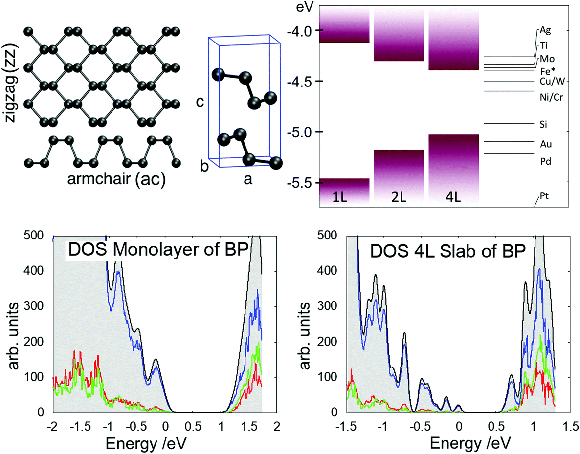 | ||
| Fig. 1 Top left: Black phosphorus monolayer and unit cell structure illustrating the lattice directions. Top right: Position of the band edges with respect to the work-function of common metals (* stainless steel). Bottom left: Total DOS of monolayer BP (grey) and projections on s-orbitals (red), p-orbitals (blue) and d-orbitals (green). Bottom right: Total DOS of multilayer BP (grey) and projections on s-orbitals (red), p-orbitals (blue) and d-orbitals (green). | ||
Intercalation energies were calculated for a four layer slab consiting of 1296 atoms (9 × 9 × 2 supercell and 20 Å vacuum gap), where the intercalated species was placed in various geometries between the second and third layer. The cohesion energy of a P atom in a monolayer of BP is 3.255 eV, in good agreement with the textbook value of 3.275 eV,31 which translates into a P–P bond energy of 2.170 eV.
To aid energy band alignment with substrates and STM tips affecting the charge state of defects, the position of the top of the valence band with respect to vacuum level was calculated as illustrated in Fig. 1. For a monolayer the VBM isat −5.5 eV, and shifts up to −5.2 eV for a bilayer and −5.0 eV for a 4 layer slab. Depending on the defect level, tip potential and applied bias the charge state of a defect can be switched, inducing a change in its electronic and geometric structure. Charge transition levels (CTLs) are calculated using defect formation energies as a function of the Fermi level position.
Defect formation energies (DFE) are calculated using:
 | (1) |
Two P chemical potentials were used: the potential of a P atom in a monolayer of BP (μP = −179.23 eV) and the chemical potential of an isolated P atom in vacuum (μP = −175.98 eV). The first is used in all previous studies summarised in Table 1. The second provides a more intuitive understanding of energies involved in breaking and creating bonds in the BP monolayer and in several layers. Since all atom positions are equivalent by symmetry, the average energy per atom can be used as P chemical potential. The difference in energy per P atom between bulk and monolayer BP is less than 0.05 eV, showing that calculated DFEs have a small dependence on choice of BP reference. Chemical potentials for iodine and oxygen were calculated as half of the energy of a I2 and O2 (triplet) molecules. For Sn and TMs the energy of an isolated atom in vacuum was used for the chemical potential. These potentials were chosen since they most resemble the conditions under crystal growth, during which impurities are incorporated – oxygen and iodine exist in their molecular form, whereas the metals are considered as isolated gaseous atoms. To calculate the incorporation energies of substitutional defects, the chemical potential of the substituted P was chosen as the energy of a P atom in monolayer BP. Thus, the incorporation energy reflects a process during crystal growth, where the substituted P atom can be moved to a new P lattice site.
| Defect | μ P(ML) | μ P(gas) | Literature |
|---|---|---|---|
| a Independent of phosphorus chemical potential. | |||
| 59 MV | 1.81 | 5.07 | 1.63,33 1.65,24 1.7126 |
| 5656 MV | 2.38 | 5.3 | 2.05,24 2.026 |
| P i | 1.91 | −1.35 | 1.7933 |
| P ads | 1.56 | −1.69 | 1.634 |
| 5757 DV | 1.51 | 8.02 | 1.3524 |
| 585-A DV | 1.70 | 8.21 | 1.36,33 1.41,24 1.7726 |
| 555777 DV | 2.85 | 9.36 | 2.28,24 2.7626 |
| 5555-6-7777 DV | 1.93 | 8.44 | 1.5424 |
| 5959 DV | 3.45 | 9.96 | |
| 585-B DV | 3.93 | 10.44 | 3.29,24 3.226 |
| 949 DV | 3.65 | 10.16 | |
| 4-10-4 DV | 2.02 | 8.53 | 2.2726 |
| SW 1 | 1.8a | 1.8a | 1.4,33 1.62,26 1.3216 |
| SW 2 | 0.9a | 0.9a | 1.22,26 1.0116 |
| Frenkel (MV + Pi) | 3.38a | 3.38a | |
| Frenkel (MV + Pads) | 3.08a | 3.08a | |
Potential alignment in these calculations is important, since the average electrostatic potential is set to zero in DFT calculations and thus, in order to compare energies between different systems, a shift in potential between different calculations needs to be corrected for. Charge corrections were performed by running 2D periodic simulations and extrapolating defect formation energies to the N → ∞ limit using cell sizes from 5 × 5 up to 18 × 18 surface unit cells (see ESI†).
3 Results of calculations
3.1 Intrinsic defects
The main types of intrinsic point defects in BP – MVs, DVs, Stone–Wales defects and self-interstitials, will be discussed in this section. An overview of DFEs is given in Table 1 along with reported values from literature. The positions of the Kohn–Sham (KS) defect states in the band gap of a monolayer and multilayer BP are shown in Fig. 3. Line defects, such as grain boundaries, dislocations and step edges, will not be discussed in this report.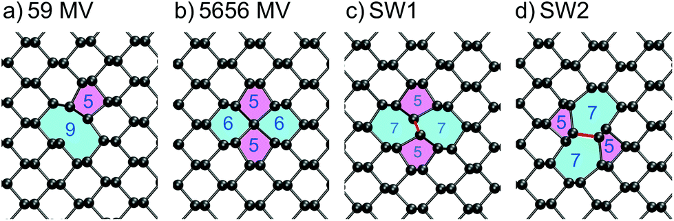 | ||
| Fig. 2 Defect structures in monolayer BP with their respective formation energies given above: (a) Neutral (5|9) phosphorus MV. (b) Negatively charged (55|66) MV. The central P atom is four coordinated in a sp3d2 hybridisation state. (c + d) Stone–Wales defects. | ||
 | ||
| Fig. 3 Schematic illustrating the defect induced Kohn–Sham states in the bandgap of BP. Filled circles indicate a filled state and empty circles an empty state, while a circle on the right/left indicates the spin up/down channel. All energies are referenced to the vacuum level (0 eV). The states for adsorbed O atom are deep in the valence band and are not shown. | ||
To investigate the electronic structure of MV, the Inverse Participation Ratio (IPR) method was used. This helps to analyse the degree of localisation and nature of defect states, with higher IPR values corresponding to higher degree of localisation of one-electron state (see the detailed description in ESI†). The IPR analysis reveals that the defect induced bandgap state is localised on the under-coordinated P atom creating a peak in the IPR spectrum. The band edge states remain delocalised as is indicated by a small IPR value. A positively charged and negatively charged vacancy were also considered and their formation energy diagram is given in ESI.† In monolayer BP, the neutral MV is the lowest energy state for Fermi levels below 0.55 eV above the VBM, after which the negative charge state becomes energetically more favourable. However, in bulk BP the negatively charged MV is most stable for all Fermi level positions.
The work-function of common metals relative to the bands of BP is indicated in Fig. 1. In recent reports Ti and Au were used as electrode contacts,12,32 which align with the VBM (Au) and the CBM (Ti). Thus, in order to establish a common Fermi level, band bending can cause defects in the vicinity of the contacts to adopt different charge states. Charged defects are also linked to lower device performance of field effect transistors made from BP and Ti/Au contacts.4 Particularly for thin BP flakes, contact with the metal substrate can shift the Fermi level position, thus inducing a change in the charge state of the MV.
The negatively charged MV adopts a significantly different geometry from the neutral state shown in Fig. 2b, where a P atom becomes sp3d2 hybridised and binds to four neighbouring P atoms, passivating all dangling bonds. The sp3d2 hybridisation is commonly observed for negatively charged phosphorus compounds such as PF6−, which allows four in-plane bonds with bond angels close to 90°. In this geometry, the four coordinated P atom sits between the top and the bottom row. There is now no acceptor state in the bandgap and the defect induced states, which appear at the band edges, show a more localised character (see Fig. 3). The IPR analysis of these states is shown in Fig. S1 in ESI.† The localised state in the conduction band can be attributed to an anti-bonding state between the four-coordinated P atom and its four nearest neighbours. The localised state near the VBM is a non-bonding state and the localised state deeper into the valence band is a bonding state between the four-coordinated atom and its four nearest neighbours. The additional potential of the negative charge leads to more localisation of deeper band states as well, which is due to constraints of the simulation cell. We note that the IPR analysis allowed us to easily identify defect-induced localised states, which would otherwise be a tedious manual checking process through all states.
The DFE for MV in a four layer slab was also calculated and the trend as the vacancy is moved into the slab investigated. While the DFE for a MV at the surface of the slab was calculated at 5.01 eV, the DFE for a MV in the second layer is 4.99 eV, which almost recovers the bulk value of 4.97 eV. The difference in formation energies for MV at the surface compared to the bulk crystal is not substantial enough to infer large differences in vacancy concentrations and vacancy aggregation at the surface can be ruled out. Thus, vacancies are expected to be distributed evenly throughout the crystal, ignoring the role of line defects in vacancy trapping.
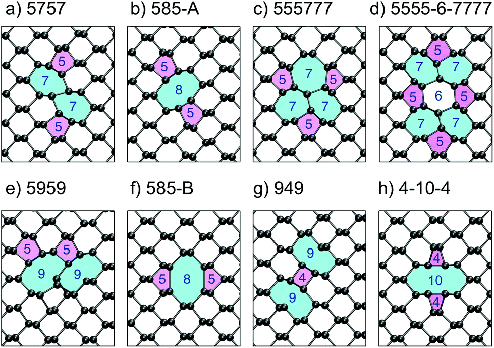 | ||
| Fig. 4 (a–h) The eight lowest energy DV structures in monolayer BP; their respective formation energies are shown in Table 1. The rings are labelled according to how many atoms make up the ring structures and are coloured as a visual aide. | ||
Apart from the 5757 vacancy, several other metastable structures were found and are shown in Fig. 4b–h. The 585-A DV has a DFE close to the 5757 one at 8.21 eV and is also more stable than two isolated MVs. Previously, this vacancy was reported to be the most stable DV structure,16,33 but recent reports16,24 as well as this work support the observation, that the 5757 structure is lower in energy. The 555777 DV shown in Fig. 4c represents a more complex DV structure and with a formation energy of 9.36 eV is still more favourable than two separate vacancies. Similar to structures a and b the atoms relax to compensate any dangling bonds created during the vacancy formation such that all atoms are three-coordinated. The 5555-6-7777 DV is very similar to the 555777 one and differs in just a rotation of a P–P bond, similar to a Stone–Wales defect. This DV configuration was found to have a lower formation energy of 8.44 eV.
We note that the ordering of the defect structures compares well with previous results,16,24 however, values of DFE in the second and forth column of Table 1 show small differences. These may result from different DFT functionals used, calculation set-up, basis set and code. Furthermore, BP is considered to be “soft” due to its low Young's modulus (166 GPa and 44 GPa along zz and ac, respectively) and thus strain due to defects in relatively small simulation cells and electrostatic interactions between periodically translated defects can lead to observed shifts in calculated formation energies. Finally we note that the lowest energy di-vacancies do not create KS states in the band gap.
Stone–Wales defects have previously been reported for graphene35,36 and theoretical calculations predict their existence in BP as well.26,33 SW defects require a change in connectivity of two atoms via a rotation of a P–P bond, which is highlighted in red in Fig. 2c + d. The formation energy of SW1 defect is 1.81 eV and of SW2 defect is 0.9 eV, which, unlike the MV case, does not rely on the choice of chemical potential for P since no atoms are added or removed, and thus can be compared to other theoretical calculations. Reported values for the SW1 defect range from 0.84 eV to 1.62 eV,16,26,33,37 highlighting a large spread in calculated DFEs, which arises from different DFT functionals, codes and calculation parameters (e.g. supercell size). The SW2 defect has the lowest DFE of the intrinsic defects considered and is thus expected to be the dominant defect formed.
In order to investigate the formation mechanism of SW defects, nudged elastic bands calculations (NEB) were performed. The forward barrier to form a SW1 defect is 3.08 eV and 2.17 eV for SW2 defect and the reverse barriers are 1.27 eV and 1.25 eV for both SW defects, respectively.
Combining the DFE for a MV and a P self-interstitial results in a Frenkel pair formation energy of 3.38 eV. This energy for MV and a surface adatom is 3.08 eV. These energies are also independent of the choice of chemical potentials used and can be directly compared to the formation energy of a Stone–Wales defect. At equilibrium conditions Frenkel defects are less favourable than SW defects.
We note that formation barriers for both SW and Frenkel defects are too high for them to be formed in high concentrations at room temperature. Instead, they can be created under high-temperature non-equilibrium growth conditions.
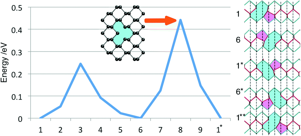 | ||
| Fig. 5 Diffusion barrier for a neutral MV along the zz direction in monolayer BP. The inset shows the transition point geometry. On the right, the geometry of the vacancy at each minima in the diffusion path is illustrated. Note the asterisk signifies a commensurate structure translated by half a unit vector and two asterisks denote a commensurate structure after translation by a whole unit vector. Red lines represent the upper and blue lines the lower zigzag. The 5 and 9 member rings are coloured in pink and cyan as a visual aid. | ||
As shown in the inset, the transition state structure is different to the symmetric structure found for the negatively charged vacancy (Fig. 2b). In the latter case, the central P atom becomes four-fold coordinated and sits in between the upper and the lower zigzag. The transition structure, however, does not show this relaxation of the central P atom and instead resembles an unrelaxed MV. In fact the four-fold coordinated geometry in its neutral charge state would be 0.1 eV higher in energy than the transition structure, which is in good agreement with ref. 24.
Interestingly, the diffusion barrier remains unchanged for a positively charged vacancy but is significantly reduced for a negatively charged vacancy. Due to the different bonding behaviour of the negative vacancy, the barrier for diffusion is lowered to ∼0.07 eV along the zz-direction. Hence a negatively charged vacancy is expected to be significantly more mobile than a neutral or positively charged vacancy.
The calculated diffusion barriers EB can be translated into hopping rates ν using an Arrhenius equation:
| ν = ν0(T)exp(−EB/kBT), | (2) |
 (N = number of hops) one can easily deduce that at room temperature on average it takes two seconds for two MVs to collide.
| Neutral MV | Negative MV | ||
|---|---|---|---|
| Temperature/K | Prefactor/s−1 | Hopping rate/s−1 | Hopping rate/s−1 |
| 300 | 1.63 × 10¹¹ | 4.49 × 10³ | 1.09 × 10¹⁰ |
| 70 | 3.81 × 10¹⁰ | 1.34 × 10⁻¹⁹ | 9.98 × 10⁵ |
| 10 | 5.44 × 10⁹ | 1.30 × 10−324 | 2.18 × 10−41 |
3.2 Extrinsic defects
Impurities are often present in BP films and have been suggested as an alternative explanation for defects observed in STM.18 Tin, which is used as a catalyst during the growth of BP crystals together with iodine, is detected in significant concentrations in XPS and inductively coupled plasma mass spectrometry (ICP-MS) measurements, as well as Ni, Zn, Fe and Cu in lower concentrations.19 These impurities were investigated here in a substitutional, intercalated and surface adsorbed geometries and their formation energies are summarised in Table 3.| Summary of defect formation energies/eV | |||
|---|---|---|---|
| Element | Adsorbed | Substitutional | Intercalated |
| Energy/eV | Energy/eV | Energy/eV | |
| O | −2.00 | −0.38 | −1.91 |
| I | 0.30 | 1.39 | 2.47 |
| Sn | −2.76 | −3.28 | −1.82 |
| Fe | −2.25 | −2.52 | −2.57 |
| Ni | −3.07 | −2.62 | −3.93 |
| Cu | −1.96 | −2.20 | −2.85 |
| Zn | −0.20 | −0.49 | −0.17 |
Tin and iodine are used as catalysts during the crystal growth and constitute the two main impurities, besides oxygen. Thus a more detailed description of these defects is given below.
Iodine was also investigated as a substitutional defect. It costs 1.39 eV to incorporate an I atom instead of lattice P, if the chemical potential of P in a BP monolayer is used as a reference. I0P binds to the 2 coordinated P atom in a P vacancy and sticks out of the surface plane (see Fig. 6). The gain in energy by forming the I–P bond is about 0.4 eV. This is in good agreement with the strength of P–I bond in PI3.38 The neutral charge state was found to be lowest in energy for all Fermi level positions throughout the bandgap and no bandgap states were created upon forming this defect. Bader analysis shows almost no charge transfer between iodine and the BP lattice, indicative of a covalent bond between P and I.
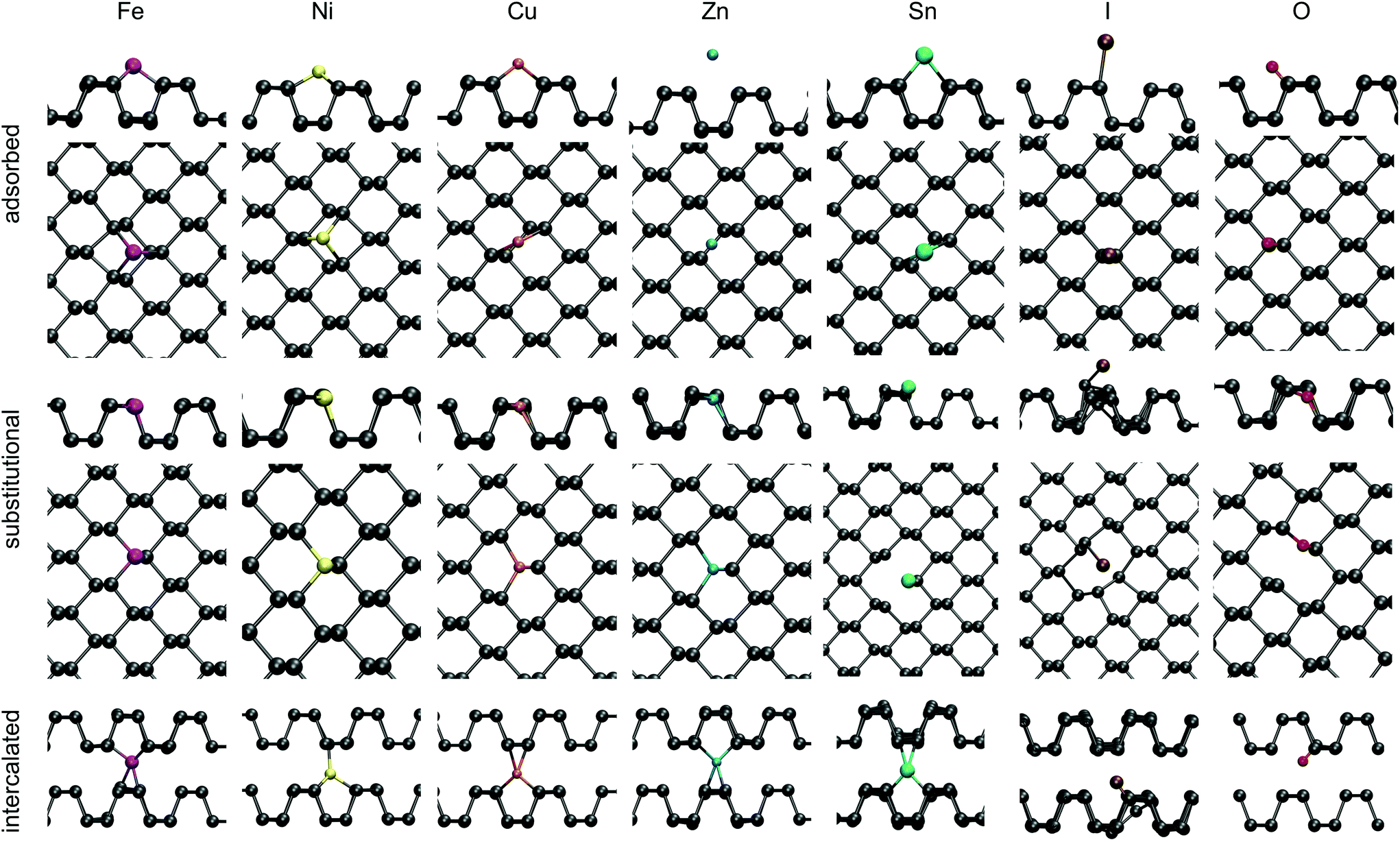 | ||
| Fig. 6 Summary of impurity defects in BP (P is grey). Geometries are shown for Fe (magenta), Ni (yellow), Cu (orange), Zn (cyan), Sn (green), I (brown) and O (red) in adsorbed (top), substitutional (middle) and intercalated (bottom) configurations. | ||
Furthermore, the intercalation energy for a single iodine atom was calculated at 2.47 eV. The relatively large I atom is not favourable to intercalate between the BP layers due to electronic overlap resulting in large lattice distortions. Whether a larger I concentration can lead to a change in interlayer spacing or a change in stacking order as has been reported for Na intercalation39 was not investigated. Finally, we note that these I-related defects do not create KS states in the BP band gap.
Only slightly smaller is the intercalation energy of an O atom at −1.91 eV, where, similarly to surface adsorption, O binds to a lone pair of a P atom with the same bond length of 1.49 Å. The difference in energy comes primarily from lattice distortions around the intercalated O atom in order to accommodate it between the 2D layers.
Comparatively less favourable is the substitution of a lattice P atom, which for a ML was calculated at −0.38 eV. The two-valent O atom can bind to one P atom of the upper row and one of the lower row, which constitutes the lowest energy configuration, or it can bind to two P atoms in the same row, which is 0.33 eV higher in energy. In both cases, a dangling bond is created, which introduces a bandgap state about 0.5 eV above the VBM (see Fig. 3), making substitution less favourable. For these calculations the reference chemical potential of oxygen was chosen as half of the energy of O2 molecule in its triplet state in vacuum. Thus the negative interaction energies corroborate with experimentally observed high reactivity of BP with molecular oxygen.40
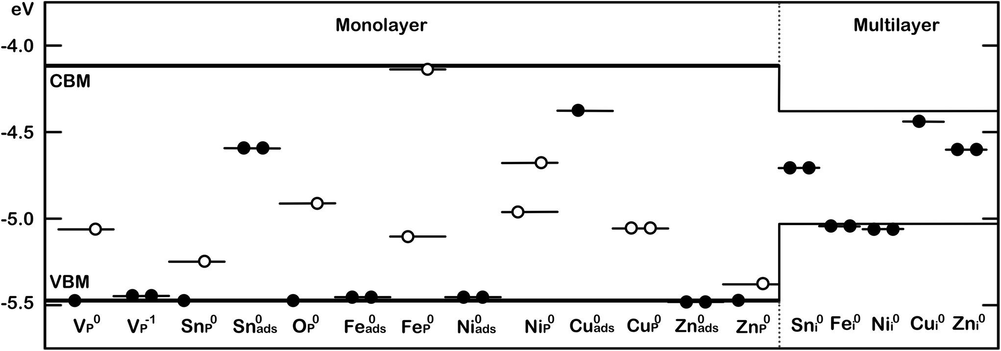
To gain insight into the defect behaviour as it is moved into the slab approaching the bulk limit, substitutional Sn impurities were investigated at various depths in a four layer slab. A four layer slab consisting of 1296 atoms was doped with a single Sn atom in the upper row of the top layer, in the bottom row of the topmost layer and similarly in the second layer. The defect formation energy decreases slightly as the Sn impurity is moved into the slab. An impurity in the top row of the top layer has a DFE of −3.50 eV, while the DFE for the second layer was reduced to −3.56 eV, indicating that substitution is slightly favoured as the defect is moved into the bulk compared to the defect at the surface or in a monolayer. A substitutional Sn in the top row of the top layer creates an acceptor state 0.15 eV above the VBM, which moves to 0.12 eV for the bottom of the top layer and ultimately to 0.05 eV for substitutional Sn in the top row of the second surface layer. This illustrates that the acceptor state becomes shallower as the defect approaches the bulk limit than that on the BP surface.
Adsorption of Sn was found to be less favourable than substitution, with an adsorption energy of −2.76 eV. Sn adsorbs 1.95 Å above the surface on top of a valley site, binding to two surface P atoms. A donor state is created in the bandgap of BP 0.43 eV below the CBM, as indicated in Fig. 3.
Lastly, intercalated Sn was investigated, with the atom placed at various positions between the second and third layer of a four layer BP slab. Sn adopts a four-valent geometry, bonding to two P atoms of the upper and lower layer, respectively. However, the BP lattice displays large displacements around the intercalated Sn, resulting in a DFE of −1.82 eV. A donor state is induced in the bandgap of BP, 0.26 eV below the CBM (see Fig. 3), which is localised on Sn. Thus, substitutional Sn acts as an acceptor, while adsorbed and intercalated Sn act as electron donors.
Intercalated TMs constitute the lowest energy configuration for the open shell elements Fe, Ni and Cu, while the closed shell Zn preferentially sits in a substitutional configuration. Upon intercalation the 4s electrons of Fe and Ni get promoted to the 3d orbitals, but for Cu and Zn the 3d shell is already completely filled and thus electrons populate the radially more extensive 4s orbital.
This rearrangement of electrons leads to changes in the magnetic moment of Ni and Fe. Since the 4s electrons completely fill the 3d orbitals in Ni defects, Ni adopts a low spin state with μB = 0. Similarly Fe changes from μB = 4 to a μB = 2 state, where the S = 5 state is 0.24 eV and the singlet state is 0.6 eV higher in energy than the triplet state. Thus Fei is predicted to possess a magnetic moment of 2μB at low temperatures. Whether the spin arrangement for higher TM concentrations leads to different magnetisation was not investigated in this work. Therefore, the results presented herein refer to low doping/impurity concentrations, where impurity atoms are dispersed. Cu induces a donor state in the bandgap of BP, which sits at the CBM and Zn induces a deep donor state 0.33 eV below the CBM. Ni and Fe, however, do not produce any bandgap states at all, as shown in Fig. 3.
Adsorbed Cu and Zn interact more weakly with BP compared to Fe and Ni as indicated by their higher respective DFEs. Cu adsorbs on a valley site between two P rows and binds to one P atom of each row with a bond length of 2.21 Å. In doing so a donor state is created at the CBM of BP. Zn also adsorbs in a valley site and binds to two surface P atoms with a bond length of 2.95 Å, but with a much reduced DFE of 0.2 eV. Fe does not exhibit the same bonding behaviour and instead binds to two P atoms of one row (2.27 Å) and one P atom of a neighbouring row (2.18 Å), sitting in a three coordinated valley site. Furthermore, as was observed for intercalated Fe, the triplet spin state is lower in energy than the singlet state, as the 4s electrons populate the 3d orbitals. The same can be observed for Ni, which also adsorbs in a three coordinated valley site with two 2.20 Å bonds to one P row and a 2.11 Å bond to the other.
Substitutional TM impurities adopt a P lattice site with a maximum relaxation of 0.26 Å along the armchair direction and 0.05 Å along the out of plane direction. Cu induces a deep acceptor state 0.42 eV above the VBM. This state is localised on the TM atom and its three nearest neighbour P atoms. The DFE for a CuP defect is −2.20 eV. Zn in contrast has a higher DFE of −0.49 eV and a small spin splitting of about 0.1 eV can be observed. This leads to an empty state in the beta (minor) spin channel at the top of the valence band, creating a shallow acceptor state. A larger spin splitting of 0.25 eV was found for the NiP defect. For both spin channels an acceptor state was created in the bandgap, which is 0.52 eV above the VBM in the spin up (major) channel and 0.77 eV above the VBM in the spin down (minor) channel. The DFE for NiP was calculated to be −2.62 eV, the lowest of the TMs considered.
Lastly, a FeP defect was considered. An isolated Fe atom has a magnetic moment of μB = 4, but upon incorporation into BP, the 4s electrons populate the 3d shell and the μB = 2 becomes lower in energy. This defect was found to have a DFE of −2.52 eV. Interestingly, an empty state is created in the spin up channel at 0.42 eV above the VBM, however, the corresponding spin down state is located at about 0.05 eV below the CBM.
It is important to note that spin splitting is very sensitive to how exchange interactions are calculated. For the calculations presented here, the proportion of exact Hartree–Fock exchange used in the density functional was fitted for a pristine BP monolayer and bulk properties and not to reproduce TM spin splitting.
4 Discussion
In order for BP to make the transition from research laboratories to everyday devices, its physical properties need to be better understood. In particular point defects play a crucial role in device stability and are still subject to extensive research. Furthermore, the introduction of extrinsic dopants can be used to functionalise BP for novel technological applications. Typically, concentrations of at least 1018 cm−3 are needed to observe doping in semiconductors and p/n-doped BP has been reported with doping concentrations of around 1015 cm−3.43 Experimentally observed p-doping has previously been attributed to MVs. However, the origin of the MVs is unclear. Their DFE is too high to be created thermally at large concentrations. MVs have low diffusion barriers and therefore can migrate and be captured by other point or line defects. Thus any MVs created during the crystal growth process have ample time to find a lower energy structure. We have shown that a MV can coalesce with another MV to form a considerably more stable DV, which does not have an acceptor state associated with it. To date there are no experimental reports of DVs on the surface of cleaved BP from scanning probe measurements, impugning the interpretation that MVs are the dominant defect.At room temperature concentrations of thermally created defects such as Frenkel pairs and SW defects are expected to be low due to their high DFEs. Thus, observed defects in experimental studies are likely defects, which are grown in during the crystal growth process or sample anneal. Since this is a non-equilibrium process, determination of accurate chemical potentials and reaction pathways is difficult. Therefore, the calculated DFE give insight into which defects are likely, but cannot be used to derive accurate defect concentrations. For example the barrier for a SW2 defect to reform into pristine BP is 1.25 eV, which means at room temperature the rate of SW annihilation is low. A detailed experimental study of defects pre and post sample anneal could be informative to investigate recombination or defect annihilation processes.
As outlined above, experimental evidence for impurity species in BP is considerable. Our results show that iodine does not react strongly with BP as P–I bonds are weak. That phosphorus reacts weakly with iodine can also be seen in the low standard enthalpy of formation of −46 kJ mol−1 (0.47 eV per molecule) for PI3, a possible intermediate reactant during crystal growth. Thus we do not expect a large concentration of I related defects in BP. Furthermore, Sn is typically added in excess to bind any iodine in Sn(IV)I4 and thus prevent reaction with BP.
Sn can be observed in XPS and ICP-MS and we have shown that substitutional Sn is the favoured configuration for Sn defects. In a BP monolayer, a shallow acceptor state 0.2 eV above the VBM is created, which moves closer to the band edge in a four layer slab. While most calculations are performed for a monolayer, most experimental data are obtained from bulk crystals or multilayer BP. Thus, our results highlight the need to consider not only monolayer systems, but also BP slabs to be able to compare with experiments directly. As the defect level becomes more shallow in multi-layer BP, it can get ionised thermally and thus creating hole carriers in BP which may be the source of observed p-doping, a process not possible for the deep acceptor state in monolayer BP.
Other dopants, which lead to p-doping are also presented: substitutional oxygen, substitutional and intercalated TMs and P self-interstitials. While most of these defects lead to p-doping, chemical analysis of BP crystals reveals an order of magnitude lower concentrations of TM elements compared to Sn.19 Thus, these are not considered to be the main contributors to p-doping. Nevertheless, results on Fe doping indicate that magnetic BP can be achieved. A Fe surface adatom as well as substitutional and intercalated Fe will adopt a spin triplet state. Our calculations represent a disperse low density limit and the long range alignment of spin for higher defect densities was not investigated. However, it has been shown experimentally that Fe doped BP crystals exhibit para-magnetism at room temperature, indicating that no long range alignment into a ferromagnetic state takes place.41
Lastly, oxygen interacts strongly with the lone pairs of phosphorus, creating O adatoms and intercalated oxygen, while substitution is less favourable. Oxygen adatoms and interstitials do not contribute to p-doping of BP, since no hole states are created, but substitutional oxygen does. However, it is unclear how a large concentration of OP defects could be created since they represent a meta-stable state almost 2 eV higher in energy than Oads and Oint.
5 Conclusions
In summary, we characterised the geometric and electronic structure of intrinsic and extrinsic point defects in BP. DFE for Frenkel pairs are higher than those for Stone–Wales type defects, which are thus assumed to be the dominant intrinsic defect. However, their DFEs are too high to be created thermally in high concentrations. Thus, observed defects are predicted to be created during the crystal growth or sample preparation process. Since these are high temperature, non-equilibrium processes, defects with high DFEs can be grown in, leading to higher defect concentrations than would be expected from their DFEs.MVs create an acceptor state in the bandgap, which is deep for a monolayer and becomes more shallow for multilayer slabs. They were also shown to have a low diffusion barrier of 0.45 eV along the surface zz-direction, leading to fast vacancy hopping at room temperature and coalescence of MVs into DVs. Unlike MVs, most DVs do not create any donor or acceptor states and thus are electronically inactive.
Extrinsic defects (I, Sn, Fe, Ni, Cu, Zn, O) were also investigated as adatoms on a monolayer, as substitutional defects and as intercalated species in a 4 layer slab, giving a comprehensive overview of experimentally reported impurities in BP. Substitutional Sn defects were found to lead to p-doping of the crystal, while Cu adatoms on the surface induce n-type behaviour. Our work provides fundamental insight into the influence of intrinsic and extrinsic point defects on the electronic properties of black phosphorus, which is imperative for future developments of BP technologies. Moreover, our findings of magnetism in BP related to vacancies and TM doping is relevant for the development of future spintronics and solotronics technologies, such as quantum memory devices, gas sensors or quantum computing applications.
Conflicts of interest
There are no conflicts to declare.References
- F. Wang, W. K. H. Ng, J. C. Yu, H. Zhu, C. Li, L. Zhang, Z. Liu and Q. Li, Appl. Catal., B, 2012, 111–112, 409–414 CrossRef CAS.
- Z. Shen, Z. Hu, W. Wang, S.-F. Lee, D. K. L. Chan, Y. Li, T. Gu and J. C. Yu, Nanoscale, 2014, 6, 14163–14167 RSC.
- H. Wang, X. Yang, W. Shao, S. Chen, J. Xie, X. Zhang, J. Wang and Y. Xie, J. Am. Chem. Soc., 2015, 137, 11376–11382 CrossRef CAS PubMed.
- L. Li, Y. Yu, G. J. Ye, Q. Ge, X. Ou, H. Wu, D. Feng, X. H. Chen and Y. Zhang, Nat. Nanotechnol., 2014, 9, 372–377 CrossRef CAS PubMed.
- H. Zhang, ACS Nano, 2015, 9, 9451–9469 CrossRef CAS PubMed.
- P. Chen, N. Li, X. Chen, W.-J. Ong and X. Zhao, 2D Mater., 2017, 5, 014002 CrossRef.
- L. Kou, T. Frauenheim and C. Chen, J. Phys. Chem. Lett., 2014, 5, 2675–2681 CrossRef CAS PubMed.
- A. N. Rudenko, S. Yuan and M. I. Katsnelson, Phys. Rev. B: Condens. Matter Mater. Phys., 2015, 92, 1–10 CrossRef.
- V. Sorkin, Y. Cai, Z. Ong, G. Zhang and Y. W. Zhang, Crit. Rev. Solid State Mater. Sci., 2017, 42, 1–82 CrossRef CAS.
- G. Wang, W. J. Slough, R. Pandey and S. P. Karna, 2D Mater., 2016, 3, 025011 CrossRef.
- Y. Huang, J. Qiao, K. He, S. Bliznakov, E. Sutter, X. Chen, D. Luo, F. Meng, D. Su, J. Decker, W. Ji, R. S. Ruoff and P. Sutter, Chem. Mater., 2016, 28, 8330–8339 CrossRef CAS.
- J. S. Kim, Y. Liu, W. Zhu, S. Kim, D. Wu, L. Tao, A. Dodabalapur, K. Lai and D. Akinwande, Sci. Rep., 2015, 5, 1–7 Search PubMed.
- V. V. Korolkov, I. G. Timokhin, R. Haubrichs, E. F. Smith, L. Yang, S. Yang, N. R. Champness, M. Schröder and P. H. Beton, Nat. Commun., 2017, 8, 1–8 CrossRef CAS PubMed.
- J. V. Riffle, C. Flynn, B. St. Laurent, C. A. Ayotte, C. A. Caputo and S. M. Hollen, J. Appl. Phys., 2018, 123, 044301 CrossRef.
- B. Kiraly, N. Hauptmann, A. N. Rudenko, M. I. Katsnelson and A. A. Khajetoorians, Nano Lett., 2017, 17, 3607–3612 CrossRef CAS PubMed.
- W. Hu and J. Yang, J. Phys. Chem. C, 2015, 119, 20474–20480 CrossRef CAS.
- Y. Guo and J. Robertson, Sci. Rep., 2015, 5, 14165 CrossRef CAS PubMed.
- Z. Qiu, H. Fang, A. Carvalho, A. S. Rodin, Y. Liu, S. J. R. Tan, M. Telychko, P. Lv, J. Su, Y. Wang, A. H. Castro Neto and J. Lu, Nano Lett., 2017, 17, 6935–6940 CrossRef CAS PubMed.
- C. C. Mayorga-Martinez, Z. Sofer, D. Sedmidubský, J. Luxa, B. Kherzi and M. Pumera, Nanoscale, 2018, 1540–1546 RSC.
- J. VandeVondele, M. Krack, F. Mohamed, M. Parrinello, T. Chassaing and J. Hutter, Comput. Phys. Commun., 2005, 167, 103–128 CrossRef CAS.
- J. VandeVondele and J. Hutter, J. Chem. Phys., 2007, 127, 114105-1–114105-9 CrossRef PubMed.
- M. Guidon, J. Hutter and J. VandeVondele, J. Chem. Theory Comput., 2009, 5, 3010–3021 CrossRef CAS PubMed.
- M. Guidon, J. Hutter and J. VandeVondele, J. Chem. Theory Comput., 2010, 6, 2348–2364 CrossRef CAS PubMed.
- Y. Cai, Q. Ke, G. Zhang, B. I. Yakobson and Y. W. Zhang, J. Am. Chem. Soc., 2016, 138, 10199–10206 CrossRef CAS PubMed.
- L. Liang, J. Wang, W. Lin, B. G. Sumpter, V. Meunier and M. Pan, Nano Lett., 2014, 14, 6400–6406 CrossRef CAS PubMed.
- X. Sun and Z. Wang, Appl. Surf. Sci., 2018, 427, 189–197 CrossRef CAS.
- J.-w. Jiang and H. S. Park, Nat. Commun., 2014, 5, 1–7 Search PubMed.
- L. Li, J. Kim, C. Jin, G. J. Ye, D. Y. Qiu, F. H. Jornada, Z. Shi, L. Chen, Z. Zhang, F. Yang, K. Watanabe, T. Taniguchi, W. Ren, S. G. Louie, X. H. Chen, Y. Zhang and F. Wang, Nat. Nanotechnol., 2016, 12, 21–25 CrossRef PubMed.
- J. Qiao, X. Kong, Z.-x. Hu, F. Yang and W. Ji, Nat. Commun., 2014, 5, 1–7 Search PubMed.
- S. Grimme, J. Antony, S. Ehrlich and H. Krieg, J. Chem. Phys., 2010, 132, 154104 CrossRef PubMed.
- J. Cox, D. Wagman and V. Mendvedev, CODATA Key Values for Thermodynamics, Hemisphere Publishing Corp., New York, 1989 Search PubMed.
- R. J. Wu, M. Topsakal, T. Low, M. C. Robbins, N. Haratipour, J. S. Jeong, R. M. Wentzcovitch, S. J. Koester and K. A. Mkhoyan, J. Vac. Sci. Technol., A, 2015, 33, 060604 CrossRef.
- Y. Liu, F. Xu, Z. Zhang, E. S. Penev and B. I. Yakobson, Nano Lett., 2014, 14, 6782–6786 CrossRef CAS PubMed.
- D. Wang, D. Han, X.-B. Li, N.-K. Chen, D. West, V. Meunier, S. Zhang and H.-B. Sun, Phys. Rev. B, 2017, 96, 155424 CrossRef.
- K. N. Kudin, B. Ozbas, H. C. Schniepp, R. K. Prud'homme, I. A. Aksay and R. Car, Nano Lett., 2008, 8, 36–41 CrossRef CAS PubMed.
- J. Ma, D. Alfè, A. Michaelides and E. Wang, Phys. Rev. B: Condens. Matter Mater. Phys., 2009, 80, 033407 CrossRef.
- M. Umar Farooq, A. Hashmi and J. Hong, Sci. Rep., 2015, 5, 1–11 Search PubMed.
- T. E. Heil, C. E. Check, K. C. Lobring and L. S. Sunderlin, J. Phys. Chem. A, 2002, 106, 10043–10048 CrossRef CAS.
- X.-f. Yu, H. Ushiyama and K. Yamashita, Chem. Lett., 2014, 43, 1940–1942 CrossRef.
- Y. Wang, B. Yang, B. Wan, X. Xi, Z. Zeng, E. Liu, G. Wu, Z. Liu and W. Wang, 2D Mater., 2016, 3, 035025 CrossRef.
- X. Jiang, X. Zhang, F. Xiong, Z. Hua, Z. Wang, S. Yang, X. Jiang, X. Zhang, F. Xiong, Z. Hua and Z. Wang, Appl. Phys. Lett., 2018, 112, 192105 CrossRef.
- H. Wang, S. Zhu, F. Fan, Z. Li and H. Wu, J. Magn. Magn. Mater., 2016, 401, 706–710 CrossRef CAS.
- H. Liu, Y. Du, Y. Deng and P. D. Ye, Chem. Soc. Rev., 2015, 44, 2732–2743 RSC.
Footnote |
| † Electronic supplementary information (ESI) available. See DOI: 10.1039/C8NR06640J |
| This journal is © The Royal Society of Chemistry 2018 |