
 Open Access Article
 This Open Access Article is licensed under a Creative Commons Attribution-Non Commercial 3.0 Unported Licence
Low-defectiveness exfoliation of MoS2 nanoparticles and their embedment in hybrid light-emitting polymer nanofibers†
Alberto
Portone
ab,
Luigi
Romano
ab,
Vito
Fasano
a,
Riccardo
Di Corato
 ac,
Andrea
Camposeo
b,
Filippo
Fabbri
d,
Francesco
Cardarelli
e,
Dario
Pisignano
bf and
Luana
Persano
b
ac,
Andrea
Camposeo
b,
Filippo
Fabbri
d,
Francesco
Cardarelli
e,
Dario
Pisignano
bf and
Luana
Persano
b
aDipartimento di Matematica e Fisica ‘Ennio De Giorgi’, Università del Salento, via Arnesano, I-73100 Lecce, Italy
bNEST, Istituto Nanoscienze-CNR, Piazza San Silvestro 12, I-56127 Pisa, Italy. E-mail: luana.persano@nano.cnr.it
cCenter for Biomolecular Nanotechnologies (CBN), Istituto Italiano di Tecnologia, Via Barsanti, I-73010 Arnesano (LE), Italy
dCenter for Nanotechnology Innovation @NEST, Istituto Italiano di Tecnologia, Piazza San Silvestro 12, I-56127 Pisa, Italy
eNEST, Scuola Normale Superiore, Piazza San Silvestro 12, I-56127 Pisa, Italy
fDipartimento di Fisica, Università di Pisa, Largo B. Pontecorvo 3, I-56127 Pisa, Italy. E-mail: dario.pisignano@unipi.it
First published on 15th November 2018
Abstract
Molybdenum disulfide (MoS2) has been attracting extraordinary attention for its intriguing optical, electronic and mechanical properties. Here, we demonstrate hybrid, organic–inorganic light-emitting nanofibers based on MoS2 nanoparticle dopants obtained through a simple and inexpensive sonication process in N-methyl-2-pyrrolidone and successfully encapsulate the nanofibers in polymer filaments. The gentle exfoliation method used to produce the MoS2 nanoparticles results in low defectiveness and preserves the stoichiometry. The fabricated hybrid fibers are smooth, uniform and flawless and exhibit bright and continuous light emission. Moreover, the fibers show significant capability for waveguiding self-emitted light along their longitudinal axes. These findings suggest that emissive MoS2 fibers formed by gentle exfoliation are novel and highly promising optical materials for sensing surfaces and photonic circuits.
1. Introduction
Layered molybdenum disulfide (MoS2)1–4 is a quasi-two-dimensional material with covalent in-plane bonds and weak out-of-plane van der Waals interactions. Such transition metal dichalcogenides show highly interesting semiconducting properties,5 including sizable direct band gap (1.2–2.2 eV),2,6,7 and can be easily intercalated, making them potentially useful for a variety of electronic applications.3,8,9 MoS2 nanoparticles (NPs) isolated or interspersed within flakes show quantum confinement effects, with a blue-shift in photoluminescence (PL) upon crystal size reduction,7,10 along with excitation-dependent PL emission.10,11 Combined with the potentially improved brightness compared to mono- and few-layered forms,7 these properties, make MoS2 NPs highly attractive for the realization of tunable light sources and optical sensors.Embedding such materials in hybrid polymer architectures such as microspheres or fibers would offer additional advantages, including the easier manipulation of functional NPs, their integration in flexible optoelectronic components, and improved stability.12–15 For instance, fibers with diameters up to few micrometers, which can be straightforwardly electrospun by intense electric fields (0.01–0.1 MV m−1) applied to NP–polymer solutions with sufficient degrees of entanglement,16–18 would make MoS2 dopants utilizable in photonic circuits and boards, including arrays of optical sensors and synaptic components.19,20 The process is highly versatile once proper dispersion conditions are found for NPs, leading to either individual filaments or large-area mats consisting of long and flexible fibers. In previous works, both hybrid and single-component light-emitting materials showed quantum yields higher than those of corresponding conjugated polymer films along with chain alignment and optical anisotropy.21–23 In addition, electrostatically interacting molecular systems with intercoupled optomechanical properties have been demonstrated.24 The encapsulation of MoS2 flakes in carbon fibers has been explored as a strategy to realize anodes for high-performance batteries.25,26 However, the emission properties of these compounds in polymer nanofibers and their application in prototypical photonic components have not been studied.
Focusing on optical properties, in this study, we introduce light-emitting fibers based on MoS2 NPs interspersed in flakes and electrospun jointly with a poly(methyl methacrylate) (PMMA) matrix. The NPs are obtained through gentle exfoliation, which is found to reduce the MoS2 particle size in all three spatial dimensions while preserving the low defect concentration and stoichiometry, as highlighted by micro-Raman mapping. The resulting fibers have smooth surfaces, exhibit uniform and bright broadband emission, and are capable of guiding generated light along their length. Thus, the fibers represent a novel hybrid material that can be promptly utilized to build optical circuits based on miniaturized waveguides and integrated sensing regions.
2. Experimental methods
MoS2 NPs were produced via the exfoliation of the bulk powder (Aldrich, particle size <2 μm) by ultrasonication for 8 h in N-methyl-2-pyrrolidone (NMP). Following the sonication step, centrifugation at 1000 rpm was carried out for 45 min to remove bulk residues and collect the supernatant. The resulting particles were inspected optically by confocal and UV-Vis spectroscopy, and morphologically by scanning electron microscopy (SEM) and transmission electron microscopy (TEM), and chemically by energy-dispersive X-ray spectrometry (EDS).Confocal analysis was performed on vacuum-dried drops (50 μL) cast from the achieved dispersion, placed onto a glass substrate and excited with a cw laser at wavelength λ = 488 nm. Micro-Raman experiments were carried out using a Renishaw InVia spectrometer equipped with a confocal optical microscope and a 532 nm excitation laser. PL lifetime measurements were performed in confocal mode by exciting light-emitting fibers with a 470 nm pulsed diode laser at 40 MHz. Signals were collected by a time-correlated single-photon counting setup. Full details on the experimental methods, including the realization of electrospun hybrid fibers, are reported in the ESI.†
3. Results and discussion
We produced MoS2 NPs by exfoliating the bulk powder via ultrasonication in NMP and subsequent centrifugation. The high surface tension of NMP (40 mJ m−2), which roughly matches the estimated surface energy of few-layered MoS2 (46.5 mJ m−2), allows a stable dispersion to be obtained.27–30 In addition, the exfoliation process is simple and environmentally friendly. The process is driven by sonochemical cavitation phenomena via the formation and implosive collapse of gas bubbles. The resulting increase in local temperature and pressure favors exfoliation and eventually lead to the formation of nanosized particles.Representative SEM images of the obtained MoS2 samples covered by few-nm-thick metal layers to facilitate inspection are shown in Fig. 1a. The images show layered flakes with transverse sizes up to a few micrometers and decorated with 20–80 nm particles (inset of Fig. 1a). The elemental compositions of both the flakes and particles were evaluated by EDS (Fig. S1 in the ESI†) and are highlighted by a sharp and intense peak at 2.3 keV, which is attributed to the presence of the transition metal dichalcogenide.31,32
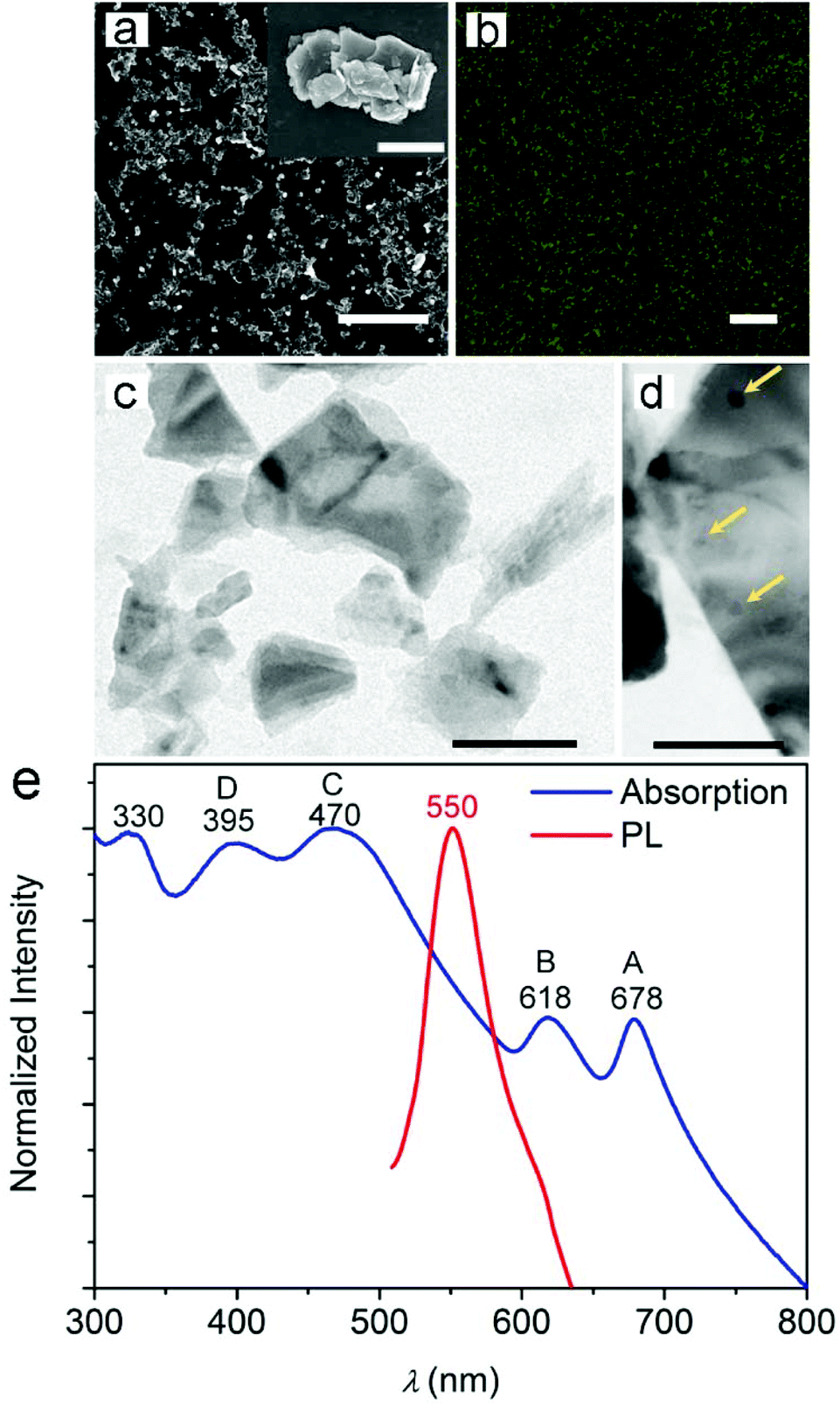 | ||
| Fig. 1 (a) SEM micrograph of MoS2 particles following exfoliation. Scale bar = 5 μm. The inset shows a representative single aggregate of particles at higher magnification. Scale bar = 1 μm. (b) Confocal fluorescence micrograph of a drop-cast MoS2 dispersion. Scale bar = 10 μm. (c, d) TEM micrographs of MoS2 following exfoliation. MoS2 NPs with diameters down to 10 nm are highlighted by yellow arrows. Scale bar = 100 nm (c) and 50 nm (d), respectively. (e) Absorbance (blue line) and PL emission spectra (red line) of the MoS2 dispersion. | ||
The PL emission from cast samples appears in the form of bright spots (Fig. 1b) with a maximum intensity at 550 nm and full width at half maximum (FWHM) of 56 nm. These characteristics are typical of the fluorescence spectrum of MoS2 particles with nm-scale lateral dimensions.7,11,33 Indeed, the formation of small fragments during sonication is generally associated with a blue-shift in emission around 450–600 nm, depending on the lateral size of the formed fragments and on the excitation wavelength. Upon excitation at 488 nm, the PL peak at 550 nm can be attributed to MoS2 NPs with lateral dimensions up to a few tens of nm.7,10,11,33 This is also supported by the TEM images shown in Fig. 1c and d, which provide evidence for the formation of few-layered MoS2 flakes and show almost round-shaped NPs with diameters down to 10 nm.
To investigate the properties of the NPs more in depth, we measured the UV-Vis absorption spectra of the liquid dispersion of MoS2 after centrifugation. The absorbance spectrum (Fig. 1e) shows characteristic features of MoS2 NPs and nanosheets, with two peaks between 600 and 700 nm and a broad band with two peaks at 395 and 470 nm.10,34 The two low-energy absorption peaks (A and B in Fig. 1e) are known to correspond to excitonic transitions and occur between the splitted valence bands and the conductance band at the K-point of the Brillouin zone of MoS2 nanosheets.7 The measured extinction coefficient at 678 nm is 412 mL mg−1 m−1 (Fig. S2†). Through quasiparticle self-consistent GW calculations, energy differences between the splitted valence bands of 146 and 174 meV have been predicted for MoS2 monolayers and bilayers, respectively, due to spin–orbit coupling and interlayer interaction.35 Here, the energy gap of about 175 meV between the A and B transitions is therefore consistent with the formation of few-layered flakes. Additional absorption peaks at 470 nm (C in Fig. 1e) and 395 nm (D) are regarded to be associated with transitions involving other regions with high density of state,36–38 as from the deep valence band to the conduction band.10,39 On the whole, peaks A–D are typical features of exfoliated MoS2. Moreover, an absorption peak in the UV spectrum (at about 330 nm) can be clearly seen in Fig. 1e. This peak is attributed to the formation of NPs with small sizes in the dispersion and consequent quantum confinement effects.7,10,11,39 These results are collectively in agreement with previous findings suggesting how exfoliation procedures might lead to complex dispersions of heterodimensional MoS2 nanostructures.
The effects of the ultrasonication process on the MoS2 bulk powder can be better analyzed by Raman spectroscopy. Fig. 2a compares the Raman spectra of the MoS2 pristine powder (blue line) and the NPs after the exfoliation process (red line). Both spectra exhibit two peaks: the E2g peak corresponding to the in-plane vibrational mode and the A1g peak related to the out-of-plane vibrational mode.
 | ||
| Fig. 2 (a) Raman spectra of bulk MoS2 (blue spectrum) and a drop-cast MoS2 dispersion after the exfoliation process (red spectrum) acquired using a 532 nm laser. The spectra are vertically shifted for clarity. (b, c) Maps of the Raman mode spacing (b) and of the E2g–A1g intensity ratio (c) acquired for the drop-cast dispersion (map size = 19 × 19 μm2). | ||
The MoS2 pristine powder shows the characteristic E2g and A1g Raman modes at 376.8 and 403.2 cm−1, respectively. The corresponding vibrational modes in the exfoliated MoS2 nanocrystals are shifted up to 381.6 and 406.8 cm−1, respectively. The stiffening of the Raman modes is likely attributed to the nanoscale size of MoS2 in all three spatial dimensions following the exfoliation process. Indeed, this particular effect has been previously reported for 18 nm MoS2 nanocrystals.7 In addition, the spectral spacing between the E2g and A1g modes (25.2 cm−1) confirms that our MoS2 consist of six to 10 layers.40 The pristine powder exhibits a corresponding Raman mode spacing equal to 26.4 cm−1, in agreement with the value of bulk MoS2.40 Interestingly, the intensity ratio between the E2g and A1g modes, which is often employed as a benchmark of the stoichiometry and defectiveness of MoS2,41,42 is similar in both spectra (∼0.5). This characteristic is especially relevant for using the achieved dispersions to build light-emitting components since it highlights that the exfoliation process does not worsen the material in terms of sulfur understoichiometry42 or increased defects.43
To evaluate the homogeneity of the achieved dispersion of NPs, we also carried out Raman mapping on an area of about 360 μm2 following drop casting on a glass substrate. Fig. 2b and c show the maps of the Raman mode spacing and of the E2g–A1g intensity ratio, respectively. Fig. S3† shows the control maps for the pristine MoS2 powder, which clearly highlight that the initial system is composed of bulk material with good homogeneity in terms of sulphur stoichiometry. In contrast, the Raman mode spacing map in Fig. 2b demonstrates that the system obtained after ultrasonication is homogeneously composed by few-layer MoS2 nanocrystals with minor bulk residues. As shown in Fig. 2c, defective areas in which the intensity ratio between the E2g and A1g modes is below 0.5 are very small within the intensity ratio map (∼7% of the analyzed region).
Fibers embedded in the MoS2 NPs as dopants were prepared by electrospinning after dissolving the polymer matrix in a complex dispersion (see ESI† for details). The resulting hybrid fibers (Fig. 3a) are uniform with average diameters around 1.6 μm and smooth surfaces (Fig. S4†). Confocal fluorescence imaging revealed a uniform PL intensity along the longitudinal axis of each fiber (Fig. 3b), suggesting the homogenous incorporation of MoS2 in the filaments. This finding is further supported by the 3D reconstruction of fibers obtained by Z-axis scanning (i.e., perpendicular to the substrate on which the fibers are deposited; inset of Fig. 3b).
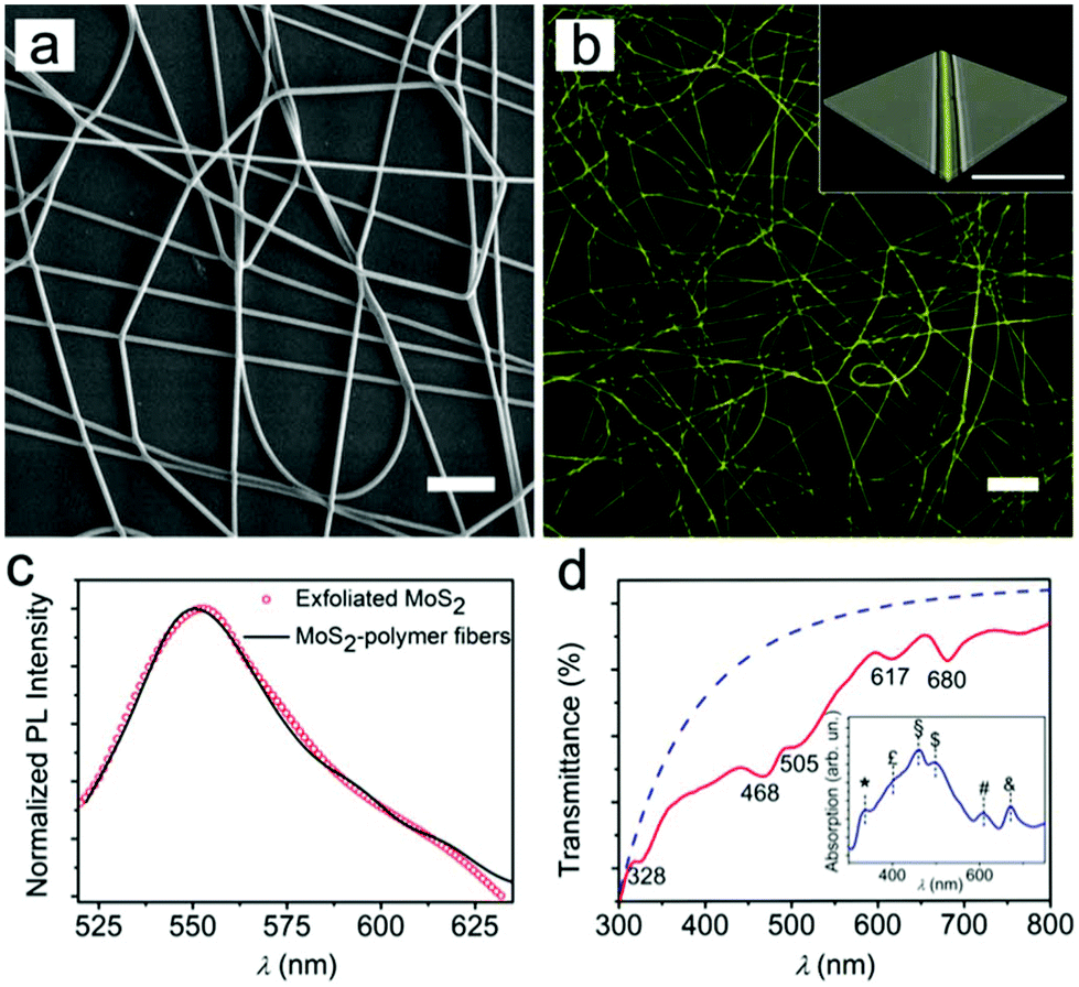 | ||
| Fig. 3 (a) SEM micrograph of MoS2-doped fibers. Scale bar = 20 μm. (b) Fluorescence confocal micrograph of fibers. Scale bar = 20 μm. The inset shows a 3D reconstruction of merged fluorescence and transmission confocal micrographs of an individual fiber by Z-axis scanning. Scale bar = 10 μm. (c) PL emission spectra of exfoliated MoS2 drop-cast on glass (red circles) and MoS2-polymer fibers (black line). The PL peak is at about 550 nm. (d) Transmittance spectrum of aligned fibers. The blue dashed line is the calculated scattering background (∼λn with n = −3.66). Inset shows the scattering background-corrected absorption spectrum. Peaks are at 336 (*), 401 (£), 460 (§), 497 ($), 611 (#) and 673 nm (&). | ||
Fig. 3c compares the PL intensities of the achieved MoS2 particles and fibers. No significant difference in emission is observed, indicating that emission was well preserved upon electrospinning. Similarly, the absorbance spectrum (Fig. 3d) indicates that the characteristic features of MoS2 are generally well preserved in the fibers, including the UV component at about 330 nm. This allows one to conclude that the NPs are effectively embedded in the hybrid fibrous material.
In fact, reduced transmission is also indicative of remarkable light-scattering phenomena arising in the fibrous sample, which can be straightforwardly taken into account as being proportional to the nth-power of the wavelength, with −4 < n < −1 (dashed line in Fig. 3d).34,37 Once such a light-scattering component is considered, fiber absorption also shows features that can be ascribed to the C (at ∼460 nm) and D (∼400 nm) transitions of MoS2 (upon more significant layering in the polymer matrix), together with an additional peak at 496 nm, which is also likely to be related to the aggregation of larger MoS2 flakes in the filaments (inset of Fig. 3d). In this respect, the polymer fibers represent an interesting environment in which the edge and quantum effects44 of exfoliated two-dimensional materials can be obtained within confined volumes.
To study the PL lifetime of the MoS2-doped fibers, we used time-correlated single-photon counting detection. The observed PL lifetime (Fig. 4a) displays a decay with an average characteristic time of (3.1 ± 0.1) ns. This result is comparable to the values reported in previous works, in which observed lifetimes typically ranged from 1.5 to 5.9 ns.10,11,45–47 The lifetime map in the inset of Fig. 4a shows a homogeneous green color along all the fibers, indicating that the average lifetime is uniform in all the filaments. Notably, the acquired data are best represented by fitting to a biexponential model with associated lifetimes of (1.3 ± 0.1) ns and (4.4 ± 0.3) ns and fractional contributions of 60% and 40%, respectively. The quality of the fit was assessed by the goodness of the obtained residuals (the monoexponential- and biexponential-derived residuals are reported in Fig. 4b as green dots and a blue line, respectively). Such biexponential behavior is not surprising and has been reported by others for MoS2 NPs.10,11 This phenomenon might depend on the presence of different species of MoS2 nanostructures within the fibers.10 In fact, heterodimensional MoS2 nanostructures present different lifetimes.45
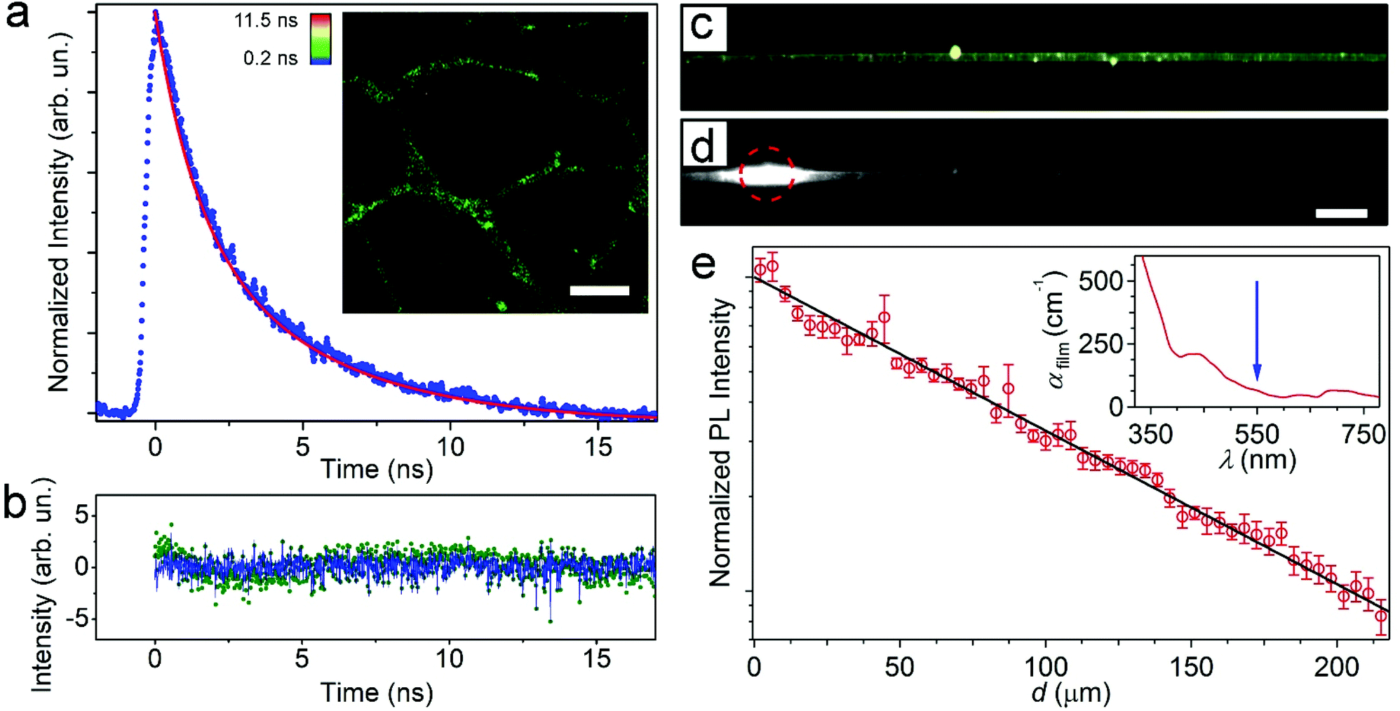 | ||
| Fig. 4 (a) Fluorescence lifetime of MoS2-doped fibers. The data are fitted using a biexponential decay model (red line). The inset shows an average lifetime map obtained by fitting the fluorescence decay curve in each pixel of the image. Scale bar = 10 μm. (b) Residuals of the monoexponential (green dots) and biexponential (blue line) fittings. (c) Fluorescence micrograph of a freestanding MoS2-doped fiber. Bright spots are associated with particle clusters. (d) PL of the same fiber during excitation by a focused laser beam (red circle in the left part of the image). Scale bar = 10 μm. (e) Spatial decay of light intensity guided inside the fiber vs. distance d from the photoexcitation spot. The continuous line is the best fit to an exponential decay according to the function I = I0−αd. The inset shows the wavelength dependence of propagation loss in a reference film doped with MoS2. The vertical arrow highlights the analyzed emission wavelength (∼550 nm). | ||
Finally, the waveguiding features of the MoS2-doped, light-emitting fibers were analyzed by microphotoluminescence (μ-PL) using suspended fibers (Fig. 4c) to avoid any optical loss induced by the substrate/fiber interface. To assess the propagation losses for light emitted by MoS2 NPs and channeled along individual hybrid filaments, the intensities of PL escaping from the fiber surface and from the tip were imaged and measured as a function of the distance (d) of the tip from the excitation spot. Fig. 4d shows a typical PL image of the fiber under excitation by a focused laser beam (red circle). The spatial decay of the self-waveguided emission is displayed in Fig. 4e. The continuous line is the best fit of the experimental data by an exponential function, IPL = I0![[thin space (1/6-em)]](https://www.rsc.org/images/entities/char_2009.gif) exp(−αd), where IPL is the PL intensity, I0 is a pre-exponential factor that indicates the intensity measured at very small d values, and α is the loss coefficient. The fits lead to α = 110 cm−1, roughly corresponding to a light transport length of 90 μm, and losses that are significantly lower than reported for other hybrid nanofibers (e.g., those doped with CdSe quantum dots) and in line with the best values found in conjugated polymer nanofibers.48,49 Theoretically, for PMMA nanofibers in air, optical losses affecting photons carried along the length of the waveguide are calculated by considering Rayleigh scattering from the nanofiber surface roughness (a few nanometers, as measured by atomic force microscopy) and are expected to be in the range 10–100 cm−1.48,50 The optical losses for photons carried along the hybrid fiber can be also attributed to self-absorption by the active component (i) along with light-scattering from either bulk (ii) or surface (iii) defects or inhomogeneities. The contribution of absorption from the polymer matrix to optical loss can be neglected as it is on the order of 10−3–10−2 cm−1 in the visible range.51
exp(−αd), where IPL is the PL intensity, I0 is a pre-exponential factor that indicates the intensity measured at very small d values, and α is the loss coefficient. The fits lead to α = 110 cm−1, roughly corresponding to a light transport length of 90 μm, and losses that are significantly lower than reported for other hybrid nanofibers (e.g., those doped with CdSe quantum dots) and in line with the best values found in conjugated polymer nanofibers.48,49 Theoretically, for PMMA nanofibers in air, optical losses affecting photons carried along the length of the waveguide are calculated by considering Rayleigh scattering from the nanofiber surface roughness (a few nanometers, as measured by atomic force microscopy) and are expected to be in the range 10–100 cm−1.48,50 The optical losses for photons carried along the hybrid fiber can be also attributed to self-absorption by the active component (i) along with light-scattering from either bulk (ii) or surface (iii) defects or inhomogeneities. The contribution of absorption from the polymer matrix to optical loss can be neglected as it is on the order of 10−3–10−2 cm−1 in the visible range.51
The contributions [(i) + (ii)] of absorption and Rayleigh scattering by bulk defects, which are mainly related to the difference in refractive index between the polymer and inorganic fillers, can be determined by measuring losses for an optical beam propagating through a film of known thickness with the same composition as the nanofibers. The inset of Fig. 4e shows the spectrum of losses (αfilm) for UV-visible light passing through such a reference film. These data allow one to estimate the losses due to MoS2 self-absorption and bulk scattering at the peak emission wavelength (about 550 nm) to be about 70 cm−1. Additional waveguiding losses directly related to the structure and defects of MoS2-polymer filaments are therefore limited to a few tens of cm−1. This further demonstrates that these fibers are uniform and free of defects and suggests that they are highly promising building blocks for optical circuits and ports.
For instance, light scattering from inhomogeneities along the fiber axis could be promoted by clusters of particles, as indicated by the bright spots shown in Fig. 4c and d. The typical distance between consecutive light-scattering spots in the μ-PL micrographs is indeed of a few μm, which agrees well with the inter-cluster distance determined by the STEM imaging of the hybrid fibers (Fig. 5).
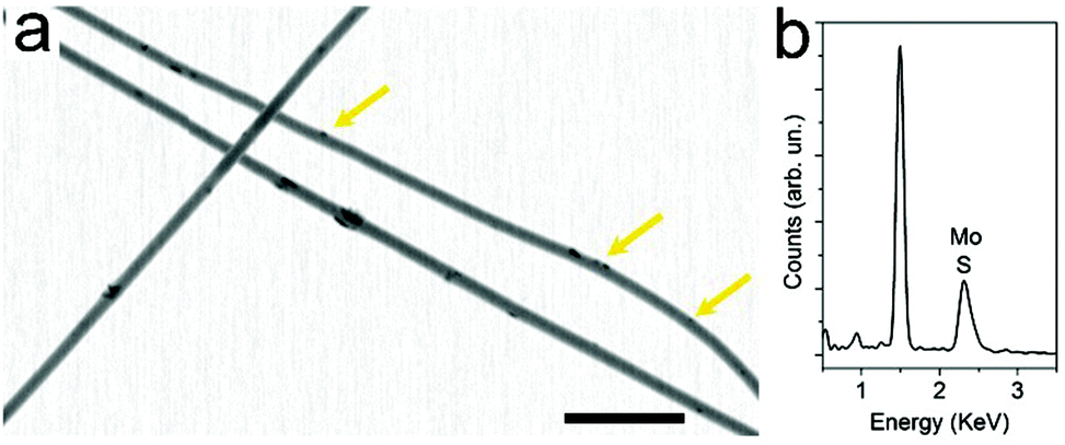 | ||
| Fig. 5 (a) STEM micrograph of hybrid nanofibers. Interspersed particles and aggregates are clearly visible (some are highlighted by yellow arrows). Scale bar = 10 μm. The corresponding EDS profile is shown in (b). The peak at 1.5 keV corresponds to aluminum in the foil used as a collector for fiber deposition. | ||
4. Conclusions
In conclusion, we produced MoS2 NPs with a simple and inexpensive ultrasonication process and realized hybrid fibers based on these NPs. The exfoliation strategy reduces the MoS2 powder size in all three spatial dimensions while preserving the low defect concentration and homogeneity in terms of sulphur stoichiometry. MoS2 is then homogeneously encapsulated in electrospun polymer filaments, which are smooth and uniform and show photonic functionality (i.e., waveguiding capability of the self-emitted light along the longitudinal fiber axis). The advantages of hybrid photonic systems based on MoS2 over light-emitting nanocomposites embedded with well-established semiconducting quantum dots might be numerous, particularly in terms of excitation-dependent emission features and low cytotoxicity,52 making them interesting for use in biomedical applications including endoscopy and optogenetics. Furthermore, the large surfaces of these dopants can be bio-functionalized through different routes,53,54 thus opening perspectives for use in diagnostic labs-on-a-chip and miniaturized chemical and optical biosensors.55 Finally, the light transport along these MoS2–polymer fibers is efficient over distances of many tens of μm. As they enable photon channeling over length scales typical of photonic chips, MoS2–polymer fibers might find applications in quantum technologies.50 By providing electromagnetic field confinement, the fibers can be exploited for the optical detection of field-interacting chemical species placed near the waveguide. The fibers can also be used for coupling radiation to other active nanomaterials through the evanescent field at their surface. All these aspects make these novel optical materials highly interesting for integration in complex, system-level platforms for sensing and in flexible optoelectronics.Conflicts of interest
There are no conflicts to declare.Acknowledgements
The research leading to these results has received funding from the European Research Council under the European Union's Seventh Framework Programme (FP/2007-2013)/ERC Grant Agreement no. 306357 (ERC Starting Grant “NANO-JETS”). D. P. also acknowledges the support from the project PRA_2018_34 (“ANISE”) from the University of Pisa.References
- K. F. Mak, C. Lee, J. Hone, J. Shan and T. F. Heinz, Phys. Rev. Lett., 2010, 105, 136805 CrossRef PubMed.
- Q. H. Wang, K. Kalantar-Zadeh, A. Kis, J. N. Coleman and M. S. Strano, Nat. Nanotechnol., 2012, 7, 699 CrossRef CAS PubMed.
- B. W. Baugher, H. O. Churchill, Y. Yang and P. Jarillo-Herrero, Nano Lett., 2013, 13, 4212 CrossRef CAS PubMed.
- W. Zhu, T. Low, Y. H. Lee, H. Wang, D. B. Farmer, J. Kong, F. Xia and P. Avouris, Nat. Commun., 2014, 5, 3087 CrossRef PubMed.
- B. Radisavljevic, A. Radenovic, J. Brivio, V. Giacometti and A. Kis, Nat. Nanotechnol., 2011, 6, 147 CrossRef CAS PubMed.
- A. Splendiani, L. Sun, Y. Zhang, T. Li, J. Kim, C. Y. Chim, G. Galli and F. Wang, Nano Lett., 2010, 10, 1271 CrossRef CAS PubMed.
- S. Mukherjee, R. Maiti, A. Midya, S. Das and S. K. Ray, ACS Photonics, 2015, 2, 760 CrossRef CAS.
- H. Hwang, H. Kim and J. Cho, Nano Lett., 2011, 11, 4826 CrossRef CAS PubMed.
- U. K. Sen and S. Mitra, ACS Appl. Mater. Interfaces, 2013, 5, 1240 CrossRef CAS PubMed.
- D. Gopalakrishnan, D. Damien and M. M. Shaijumon, ACS Nano, 2014, 8, 5297 CrossRef CAS PubMed.
- J. Y. Wu, X. Y. Zhang, X. D. Ma, Y. P. Qiu and T. Zhang, RSC Adv., 2015, 5, 95178 RSC.
- C. L. Zhang and S. H. Yu, Chem. Soc. Rev., 2014, 43, 4423 RSC.
- S. Y. Min, J. Bang, J. Park, C. L. Lee, S. Lee, J. J. Park, U. Jeong, S. Kim and T. W. Lee, RSC Adv., 2014, 4, 11585 RSC.
- Y. Lee, J. Y. Oh, T. R. Kim, X. Gu, Y. Kim, G. J. N. Wang, H. C. Wu, R. Pfattner, J. W. F. To, T. Katsumata, D. Son, J. Kang, J. R. Matthews, W. J. Niu, M. Q. He, R. Sinclair, Y. Cui, J. B. H. Tok, T. W. Lee, Z. N. Bao and D. Son, Adv. Mater., 2018, 30, 1704401 CrossRef PubMed.
- Y. Lee, S. Y. Min and T. W. Lee, Macromol. Mater. Eng., 2017, 302, 1600507 CrossRef.
- D. H. Reneker and I. Chun, Nanotechnology, 1996, 7, 216 CrossRef CAS.
- A. Greiner and J. H. Wendorff, Angew. Chem., Int. Ed., 2007, 46, 5670 CrossRef CAS PubMed.
- L. Persano, A. Camposeo and D. Pisignano, Prog. Polym. Sci., 2015, 43, 48 CrossRef CAS.
- S. Y. Min, T. S. Kim, B. J. Kim, H. Cho, Y. Y. Noh, H. Yang, J. H. Cho and T. W. Lee, Nat. Commun., 2013, 4, 1773 CrossRef PubMed.
- W. Xu, S. Y. Min, H. Hwang and T. W. Lee, Sci. Adv., 2016, 2, e1501326 CrossRef PubMed.
- M. V. Kakade, S. Givens, K. Gardner, K. H. Lee, D. B. Chase and J. F. Rabolt, J. Am. Chem. Soc., 2007, 129, 2777 CrossRef CAS PubMed.
- S. Pagliara, M. S. Vitiello, A. Camposeo, A. Polini, R. Cingolani, G. Scamarcio and D. Pisignano, J. Phys. Chem. C, 2011, 115, 20399 CrossRef CAS.
- M. Richard-Lacroix and C. Pellerin, Macromolecules, 2013, 46, 9473 CrossRef CAS.
- L. Persano, A. Camposeo, A. V. Terentjevs, F. Della Sala, E. Fabiano, M. Montinaro and D. Pisignano, Adv. Mater., 2017, 29, 1701031 CrossRef PubMed.
- X. Xiong, W. Luo, X. Hu, C. Chen, L. Qie, D. Hou and Y. Huang, Sci. Rep., 2015, 5, 9254 CrossRef CAS PubMed.
- C. Zhao, J. Kong, X. Yao, X. Tang, Y. Dong, S. L. Phua and X. Lu, ACS Appl. Mater. Interfaces, 2014, 6, 6392 CrossRef CAS PubMed.
- A. O'Neill, U. Khan and J. N. Coleman, Chem. Mater., 2012, 24, 2414 CrossRef.
- Y. Yao, L. Tolentino, Z. Yang, X. Song, W. Zhang, Y. Chen and C. P. Wong, Adv. Funct. Mater., 2013, 23, 3577 CrossRef CAS.
- A. P. Gaur, S. Sahoo, M. Ahmadi, S. P. Dash, M. J. F. Guinel and R. S. Katiyar, Nano Lett., 2014, 14, 4314 CrossRef CAS PubMed.
- A. Jawaid, D. Nepal, K. Park, M. Jespersen, A. Qualley, P. Mirau, L. F. Drummy and R. A. Vaia, Chem. Mater., 2015, 28, 337 CrossRef.
- L. Zhang, W. Fan, W. W. Tjiu and T. Liu, RSC Adv., 2015, 5, 34777 RSC.
- D. Zhang, J. Wu, P. Li and Y. Cao, J. Mater. Chem. A, 2017, 5, 20666 RSC.
- V. Štengl and J. Henych, Nanoscale, 2013, 5, 3387 RSC.
- J. N. Coleman, M. Lotya, A. O'Neill, S. D. Bergin, P. J. King, U. Khan, K. Young, A. Gaucher, S. De, R. J. Smith, I. V. Shvets, S. K. Arora, G. Stanton, H. Y. Kim, K. Lee, G. T. Kim, G. S. Duesberg, T. Hallam, J. J. Boland, J. J. Wang, J. F. Donegan, J. C. Grunlan, G. Moriarty, A. Shmeliov, R. J. Nicholls, J. M. Perkins, E. M. Grieveson, K. Theuwissen, D. W. McComb, P. D. Nellist and V. Nicolosi, Science, 2011, 331, 568 CrossRef CAS PubMed.
- T. Cheiwchanchamnangij and W. R. Lambrecht, Phys. Rev. B: Condens. Matter Mater. Phys., 2012, 85, 205302 CrossRef.
- R. A. Bromley, R. B. Murray and A. D. Yoffe, J. Phys. C: Solid State Phys., 1972, 5, 759 CrossRef CAS.
- A. R. Beal, J. C. Knights and W. Y. Liang, J. Phys. C: Solid State Phys., 1972, 5, 3540 CrossRef CAS.
- K. Wang, J. Wang, J. Fan, M. Lotya, A. O'Neill, D. Fox, Y. Feng, X. Zhang, B. Jiang, Q. Zhao, H. Zhang, J. N. Coleman, L. Zhang and W. J. Blau, ACS Nano, 2013, 7, 9260 CrossRef CAS PubMed.
- W. Qiao, S. Yan, X. He, X. Song, Z. Li, X. Zhang, W. Zhong and Y. Du, RSC Adv., 2014, 4, 50981 RSC.
- C. Lee, H. Yan, L. E. Brus, T. F. Heinz, J. Hone and S. Ryu, ACS Nano, 2010, 4, 2695 CrossRef CAS PubMed.
- H. Li, Q. Zhang, C. C. R. Yap, B. K. Tay, T. H. T. Edwin, A. Olivier and D. Baillargeat, Adv. Funct. Mater., 2012, 22, 1385 CrossRef CAS.
- W. M. Parkin, A. Balan, L. Liang, P. M. Das, M. Lamparski, C. H. Naylor, J. A. Rodríguez-Manzo, A. T. C. Johnson, V. Meunier and M. Drndi, ACS Nano, 2016, 10, 4134 CrossRef CAS PubMed.
- F. Fabbri, E. Rotunno, E. Cinquanta, D. Campi, E. Bonnini, D. Kaplan, L. Lazzarini, M. Bernasconi, C. Ferrari, M. Longo, G. Nicotra, A. Molle, V. Swaminathan and G. Salviati, Nat. Commun., 2016, 7, 13044 CrossRef CAS PubMed.
- C. Backes, R. J. Smith, N. McEvoy, N. C. Berner, D. McCloskey, H. C. Nerl, A. O'Neill, P. J. King, T. Higgins, D. Hanlon, N. Scheuschner, J. Maultzsch, L. Houben, G. S. Duesberg, J. F. Donegan, V. Nicolosi and N. Scheuschner, Nat. Commun., 2014, 5, 4576 CrossRef CAS PubMed.
- S. Mukherjee, R. Maiti, A. K. Katiyar, S. Das and S. K. Ray, Sci. Rep., 2016, 6, 29016 CrossRef CAS PubMed.
- W. Dai, H. Dong, B. Fugetsu, Y. Cao, H. Lu, X. Ma and X. Zhang, Small, 2015, 11, 4158 CrossRef CAS PubMed.
- H. Dong, S. Tang, Y. Hao, H. Yu, W. Dai, G. Zhao, Y. Cao, H. Lu, X. Zhang and H. Ju, ACS Appl. Mater. Interfaces, 2016, 8, 3107 CrossRef CAS PubMed.
- M. Moffa, V. Fasano, A. Camposeo, L. Persano and D. Pisignano, Proc. SPIE, 2016, 9745, 97450S CrossRef.
- V. Fasano, A. Polini, G. Morello, M. Moffa, A. Camposeo and D. Pisignano, Macromolecules, 2013, 46, 5935 CrossRef CAS PubMed.
- M. Gaio, M. Moffa, M. Castro-Lopez, D. Pisignano, A. Camposeo and R. Sapienza, ACS Nano, 2016, 10, 6125 CrossRef CAS PubMed.
- T. Kaino and Y. Katayama, Polym. Eng. Sci., 1989, 29, 1209 CrossRef CAS.
- J. H. Appel, D. O. Li, J. D. Podlevsky, A. Debnath, A. A. Green, Q. H. Wang and J. Chae, ACS Biomater. Sci. Eng., 2016, 2, 361 CrossRef CAS.
- D. Voiry, A. Goswami, R. Kappera, C. de Carvalho Castro e Silva, D. Kaplan, T. Fujita, M. Chen, T. Asefa and M. Chhowalla, Nat. Chem., 2015, 7, 45 CrossRef CAS PubMed.
- R. M. Kong, L. Ding, Z. Wang, J. You and F. Qu, Anal. Bioanal. Chem., 2015, 407, 369 CrossRef CAS PubMed.
- S. Barua, H. S. Dutta, S. Gogoi, R. Devi and R. Khan, ACS Appl. Nano Mater., 2018, 1, 2 CrossRef CAS.
Footnote |
| † Electronic supplementary information (ESI) available: Full experimental details, EDS data, further absorption and micro-Raman characterization, and the dimensional distribution of realized fibers. See DOI: 10.1039/c8nr06294c |
| This journal is © The Royal Society of Chemistry 2018 |