
 Open Access Article
 This Open Access Article is licensed under a Creative Commons Attribution-Non Commercial 3.0 Unported Licence
In situ impedance matching in Nb/Nb2O5/PtIr memristive nanojunctions for ultra-fast neuromorphic operation
Dániel
Molnár
 ab,
Tímea Nóra
Török
ab,
Botond
Sánta
ab,
Agnes
Gubicza
ac,
András
Magyarkuti
ab,
Roland
Hauert
d,
Gábor
Kiss
e,
András
Halbritter
ab and
Miklós
Csontos
*ac
ab,
Tímea Nóra
Török
ab,
Botond
Sánta
ab,
Agnes
Gubicza
ac,
András
Magyarkuti
ab,
Roland
Hauert
d,
Gábor
Kiss
e,
András
Halbritter
ab and
Miklós
Csontos
*ac
aDepartment of Physics, Budapest University of Technology and Economics, Budafoki ut 8, 1111 Budapest, Hungary
bMTA-BME Condensed Matter Research Group, Budafoki ut 8, 1111 Budapest, Hungary
cEmpa, Swiss Federal Laboratories for Materials Science and Technology, Transport at Nanoscale Interfaces Laboratory, Überlandstrasse 129, CH-8600 Dübendorf, Switzerland. E-mail: miklos.csontos@empa.ch
dEmpa, Swiss Federal Laboratories for Materials Science and Technology, Laboratory for Joining Technologies & Corrosion, Überlandstrasse 129, CH-8600 Dübendorf, Switzerland
eDepartment of Atomic Physics, Budapest University of Technology and Economics, Budafoki ut 8, 1111 Budapest, Hungary
First published on 1st October 2018
Abstract
The dynamical aspects of bipolar resistive switchings have been investigated in Nb/Nb2O5/PtIr nanojunctions. We found that the widely tuneable ON and OFF state resistances are well separated at low bias. On the other hand, the high-bias regime of the resistive switchings coincides with the onset of a high nonlinearity in the current–voltage characteristics, where the impedance of both states rapidly decreases and becomes equivalent around 50 Ω. This phenomenon enables the overriding of the RC limitations of fast switchings between higher resistance ON and OFF states. Consequently, nanosecond switching times between multiple resistance states due to subnanosecond voltage pulses are demonstrated. Moreover, this finding provides the possibility of impedance engineering by the appropriate choice of voltage signals, which facilitates that both the set and reset transitions take place in an impedance matched manner to the surrounding circuit, demonstrating the merits of ultra-fast operation of Nb2O5 based neuromorphic networks.
With the rapid development of neuromorphic computing1–4 the demand for cost and energy efficient, scalable non-volatile resistive switching elements utilizing CMOS compatible material platforms is increasing.5,6 In particular, reservoir computing paradigms7 exploiting the massive parallelism and nonlinear dynamics of complex neural networks have great potential in various autonomous applications. Their computational conception is based on the overall transient response of the network, whereas hardware functionality is encoded in the (reprogrammable) internal connections of the network nodes. Alternatively, simplified architectures consisting of a single nonlinear node, a delayed feedback loop and serial data streaming with fast time multiplexing have also been demonstrated.8,9 In either case, high speed resistive switching of the network elements adds to the aforementioned benchmark parameters.
The various forms of niobium-oxides have been shown to be excellent candidates to simultaneously satisfy the above criteria. Due to their high temperature stability, relative ease of deposition and excellent dielectric characteristics, insulating niobium oxides10 have been employed in commercial thin film capacitors for more than a decade and were also put forward recently as a basic compound in high-performance supercapacitors11,12 evidencing industrial compatibility. Moreover, the interplay of the strongly nonlinear, rectifying current–voltage (I–V) characteristics,13,14 the high mobility of oxygen vacancies15 and the tuneable oxygen vacancy storage capacity of the oxide interfaces16–19 enabled the fabrication of multilayered stacks of different NbOx compounds exhibiting combined threshold switching and memory effects.20–23 As a key technological advantage, these properties offer an inherent solution to the so-called sneak path problem and thus eliminate the need for external selector devices in crossbar memristor arrays.24
Here we demonstrate that the nonlinear I–V characteristics of Nb2O5 are also a fundamental ingredient to perform nanosecond resistive switchings even when the ON and OFF state resistances (RON, ROFF) are adjusted to higher values in order to maintain the convenience of read-out operation at a reduced energy budget. We have employed a custom built setup enabling the generation, propagation and detection of voltage pulses as short as 500 ps and applied the formalism of the telegraph equations. We show that low microwave frequency impedance values ZOFF = ZON ≈ Z0 = 50 Ω can be achieved simultaneously for both resistance states even when the low-bias relations of ROFF ≫ RON ≫ Z0 hold, provided the amplitude of the driving voltage pulses exceeds the onset of the strongly nonlinear regime in the I–V characteristics. This finding points out the technological relevance of the highly nonlinear I–V characteristics in Nb2O5 beyond delivering a built-in selector element for crossbar memristor arrays: the equivalence and tunability of ZOFF and ZON at moderate voltage levels enable ultra-fast neuromorphic circuit operation by circumventing the inherently incomplete impedance matching of the different resistance states to the circuit environment.
We studied resistive switchings in voltage biased nanojunctions created between a mechanically sharpened PtIr tip of a custom designed scanning tunneling microscope (STM) and a 20 nm thick Nb2O5 layer established on the top of a 300 nm thick sputtered Nb layer by anodic oxidation.25 This experimental arrangement, while not directly available for device integration, provides a convenient access to electrode surface areas below standard lithographical resolution, offers the versatility of the combined mechanical and electrical means of initializing resistive switchings and, thus, also helps in optimizing the design principles of future on-chip device architectures.
The growth procedure and structural characterization of the Nb2O5 thin films are illustrated in Fig. 1. Anodic oxidation was carried out in a 1% aqueous solution of H3PO4 using a stainless steel cathode and the aforementioned 300 nm thick Nb film sputtered on top of a standard Si wafer as the anode while a constant current density of 1 mA cm−2 was applied. The voltage drop across the electrodes and the corresponding oxide layer thickness are displayed in the left and right axes of Fig. 1(a), respectively. The film thickness along with the stoichiometric composition was determined by X-ray photoelectron spectroscopy (XPS) and subsequent Ar+ ion milling. The inset of Fig. 1(b) shows the XPS spectrum acquired at the surface of the sample. The Nb2O5 composition was identified on the basis of the specific binding energies of 210.4 eV and 207.7 eV corresponding to the Nb5+ 3d3/2 and 3d5/2 states, respectively. Fig. 1(b) shows the atomic concentrations of elemental Nb and O as deduced from the XPS spectra recorded between the milling steps. The sputtering time was converted to a depth profile using a standard Ta2O5 reference sample.26,27 The calibration value of the sputtering rate on Ta2O5 was 5.1 nm min−1 for 2 kV Ar+ ions.
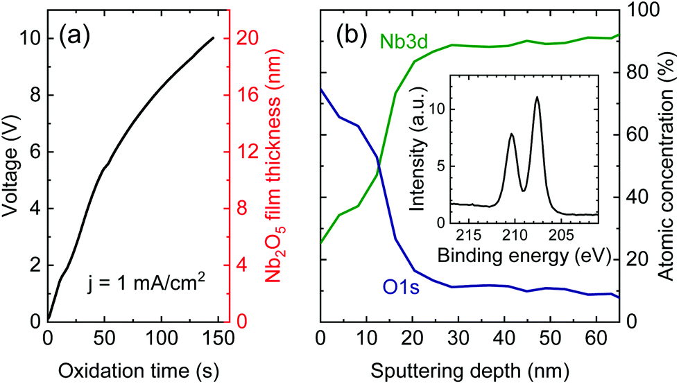 | ||
| Fig. 1 (a) Voltage drop across the Nb2O5 layer acquired during anodic oxidation (left axis) and the corresponding film thickness (right axis). (b) The depth profile of the atomic concentrations of Nb and O as determined by XPS measurements carried out between subsequent Ar+ ion milling steps of the Nb2O5/Nb structure. The inset shows the spectrum acquired at the surface of the oxide layer signalling the Nb2O5 stoichiometry. | ||
Numerous nanoscale junctions were created and tested for reproducible I–V characteristics by using the DC setup shown in Fig. 2(a). The junctions were initialized in the desired state by the current controlled, low-bias (100 mV) approaching of the STM tip to the thin film sample until a direct contact was established at a preset resistance value. This step was directly followed by I–V measurements without the application of a dedicated electroforming procedure. The first few periods were typically dominated by unstable, non-switching traces before stable resistive switching occurs. This procedure enabled the acquisition of several thousand I–V traces exhibiting stable hysteretic behavior as a function of a triangular Vdrive voltage signal acting on the junction and the RS series resistor. The role of RS was to terminate the set transition. As the resistance of the junction approaches the value of RS, an increasing (decreasing) fraction of Vdrive drops on RS (the junction), slowing down the set transition, in accordance with the data demonstrated in Fig. 2(c). Beside RS, no external current compliance was applied. As a voltage polarity convention, positive bias refers to a higher potential acting on the thin film with respect to the STM tip. The device's current was monitored by a current amplifier whereas the Vbias voltage drop on the memristor was determined numerically as Vbias = Vdrive − I·RS. All measurements were carried out at room temperature.
 | ||
| Fig. 2 (a) Schematic illustration of the STM arrangement of the nanojunction as well as the circuit diagram of the low-frequency I–V measurement setup. (b) Representative I–V trace of a Nb/Nb2O5/PtIr nanojunction with RS = 1050 Ω. The red and blue lines correspond to the zero bias slopes of the OFF and ON state I–V branches with ROFF = 91 kΩ and RON = 1.6 kΩ, respectively. The inset shows the same I–V trace on a logarithmic current scale. (c) Selected I–V traces of a different junction recorded at a frequency of fdrive = 2.5 Hz and varying amplitudes (see labels). (d) Selected I–V traces acquired at V0drive = 2.5 V amplitude and different frequencies (see labels). All traces share identical hysteresis directions as indicated by the arrows. The curves in panels (c) and (d) are vertically shifted for clarity. They were obtained on the same nanojunction connected in series with RS = 1050 Ω. | ||
A representative I–V trace recorded within 400 ms is displayed on linear and semi-logarithmic scales in Fig. 2(b) and its inset, respectively. Bipolar resistive switching typically occurs when the magnitude of Vbias exceeds ≈0.5 V at either polarity. ROFF/RON resistance ratios up to 102 are routinely obtained. The comparison of the above switching threshold and electroforming voltage values with those reported on Nb2O5 layers having similar thicknesses in ref. 16 suggests that our experimental findings do not rely on a possible, deep indentation of the tip in the oxide surface.
The onset of resistive switching behavior was further studied as a function of the V0drive amplitude and fdrive frequency of the triangular driving voltage signal as illustrated in Fig. 2(c) and (d), respectively. We found that the ROFF/RON resistance ratio increases with V0drive while it decreases with fdrive, satisfying the so-called voltage-time dilemma,28,29 the fundamental criterion of non-volatile data storage. Furthermore, Fig. 2(c) and (d) demonstrate that resistive switching in Nb2O5 is superimposed on intrinsically nonlinear I–V characteristics. Consequently, the response to high-bias driving is expected to be markedly different from the low-bias ohmic behavior of the non-volatile ON and OFF states. It is also to be emphasized that while the low-bias ON and OFF state I–V branches are well separated and exhibit slopes which can be widely adjusted by mechanical and/or electrical forming procedures, they consistently merge in the nonlinear regime as displayed in Fig. 2(b). This feature gives rise to the opportunity of the simultaneous impedance matching of both states to the circuit environment during programming and thus enables fast operation of Nb2O5 based neuromorphic circuits irrespective of the actual status of the individual network elements. In the following we focus on this nonlinear regime by inserting our memristive junctions into a waveguide circuit and exposing them to sub-nanosecond voltage pulses.
Fig. 3(a) shows the block diagram of our custom-built high-frequency setup. The PtIr tip and the Nb2O5 thin film sample are mounted on the central conductors of separate printed co-planar waveguide circuit boards sharing a common ground. The junction is created by the piezo-driven approaching of the circuit boards. Each side of the junction is connected to a custom-built unipolar rise time avalanche pulse generator30 (PGL and PGR). The layout of the pulse generators, which are implemented on identical, impedance matched co-planar waveguide boards, is shown in Fig. 3(b). The operation of PGL and PGR relies on the periodic charging (avalanche break-down) of the bipolar transistor indicated in Fig. 3(b) through the 1 MΩ resistor and the 2 pF capacitor located at the VIN terminal (50 Ω resistor at VOUT), yielding unipolar outbursts specified to a 500 ps FWHM and up to 10 V amplitude at an average repetition rate of ∼100 kHz. Such a continuous pulsing operation requires a constant VIN = 80 V input voltage in accordance with the specifications of the utilized bipolar transistor. Due to the inherently stochastic nature of the above described avalanche breakdown procedure, the timing of the individual pulses also follows a probability distribution rather than a well-defined repetition frequency. However, restricting the time window of the VIN = 80 V bias to 10 μs ensures the firing of a single 500 ps long voltage pulse. Accordingly, we employed the amplified voltage signals of further two, slower arbitrary waveform generators to independently bias PGL/PGR and trigger CH1/CH2 of our oscilloscope. The DC port shown in Fig. 3(a) is utilized for the low-voltage (350 mV) read-out of the actual resistance state of the junction between the short pulses. The transmitted and reflected voltage signals VTrans and VRefl are carried by 20 GHz bandwidth coaxial lines and acquired by the two 50 Ω matched channels of a 1 GHz bandwidth and 100 ps sampling rate digital oscilloscope.
 | ||
| Fig. 3 (a) Schematics of the high frequency pulsing setup. CH1 and CH2 indicate the 50 Ω inputs of a 1 GHz bandwidth oscilloscope. PGL and PGR are two identical, unipolar rise time avalanche pulse generators employed to facilitate the SET and RESET transitions of the nanojunction, respectively. (b) Circuit diagram of the PGL and PGR pulse generators. (c) The transmitted voltage pulse normalized to the V0OUT amplitude of the bias voltage pulse in the case of a short circuit (black), a 560 Ω resistor (green), a 2.2 kΩ resistor (brown) and a Nb/Nb2O5/PtIr nanojunction initialized at 2.6 kΩ (red). The corresponding VTrans voltage directly measured at CH1 is shown on the right axis. (d) The ROFF (red) and RON (blue) resistance values determined by applying a 350 mV DC voltage between 1000 consecutive resistive switchings. (e) Transmitted voltage signal corresponding to 10 subsequent switching pulses recorded at CH1, along with a representative, time resolved SET transition initiated by PGR (f). Note that (e) and (f) share the same voltage scale. (g) The transmitted voltage signal of a representative, time resolved RESET transition initiated by PGL and recorded at CH2. The time axes of (c), (f) and (g) are individually off-set for clarity. | ||
Fig. 3(c) shows VTrans/V0OUT and VTrans when the setup is tested with the pulse generator directly connected to Channel 1 of the oscilloscope bypassing the memristor junction (black line), as well as with commercial smd resistors (green and brown lines) inserted in the circuit. The highest transmission (VTrans = 2.55 V peak) of the 500 ps FWHM pulse is obtained under the former conditions, while the 560 Ω and 2.2 kΩ ≫ Z0 = 50 Ω resistors strongly suppress the transmission. The latter phenomenon is in quantitative agreement with the specific solution of the telegraph equations derived for our arrangement31,32 taking the forms of
 | (1) |
 | (2) |
The reproducibility of the resistive switchings is demonstrated by a sequence of 1000 pulses fired from PGL and PGR in an alternating manner. The corresponding ROFF = 2.7 ± 0.2 kΩ and RON = 430 ± 60 Ω resistance values shown in Fig. 3(d) were measured by applying a 350 mV DC offset during the 10 μs intervals between the adjacent pulses. We note that hereafter the notations R and Z refer to the low-bias DC resistance and to the voltage dependent high-frequency impedance, respectively. The raw data of a selected section of 10 pulses are highlighted in Fig. 3(e) as measured directly on Channel 1, illustrating the long term stability of the individual resistance values between the resistive switchings. Single, time-resolved set and following reset events as seen in VTrans are exemplified in Fig. 3(f) and (g), respectively. Note that during these measurements the peak values are cut off for the better resolution of the equilibrium signal levels which are reached within 8 ns (5 ns) after the onset of the FWHM = 650 ps set (reset) voltage pulses. We argue, however, that while the >1 ns long, instrumental tail superimposed on the falling edge of the main pulse [see Fig. 3(c)] obscures the unambiguous read-out of the final resistance value, its low magnitude is insufficient to further modify the resistive state of the device, in accordance with both the low-frequency data shown in Fig. 2(c) and the high-frequency data shown in Fig. 4 as we discuss later. Therefore we conceive that the actual resistive switching indeed takes place on the sub-nanosecond timescale of the FWHM, underlining the great technological potential of the so-far unprecedented switching speeds in non-volatile Nb2O5 resistive switching devices. It is also to be added that (i) according to the comparison of Fig. 3(c) with 3(f) and (g), the magnified voltage scales of Fig. 3(f) and (g) only allow us to display the aforementioned instrumental tail of the signals; and (ii) the apparent lack of symmetry between Fig. 3(f) and (g) is the consequence of the asymmetric coupling of the DC signal while PGL and PGR fire in a symmetric fashion, as indicated in Fig. 3(a).
 | ||
| Fig. 4 (a) The V0OUT peak values of the applied sequence of VOUT driving voltage pulses having a 10 ns width, alternating sign and varying amplitude. (b) Resistance values determined by a low DC voltage of 350 mV applied between the pulses. (c) The impedance of the nanojunction as a function of V0OUT as determined from the spectroscopy of the transmitted and reflected voltage pulses. The red (blue) colors of the data points in (b, c) indicate the negative (positive) polarity of the preceding voltage pulse. As a guide to the eye, the horizontal black line corresponds to Z = 50 Ω. | ||
Next we investigated in detail the enhanced microwave frequency transmission arising from the nonlinear I–V characteristics by applying variable amplitude voltage pulses of 10 ns width and alternating sign to the nanojunction. For this purpose we employed a single 250 MHz bandwidth arbitrary waveform generator as a voltage source and measured the applied VOUT, the transmitted VTrans and reflected VRefl voltage signals via the 50 Ω impedance matched input channels of our 1 GHz bandwidth oscilloscope. The varying amplitudes of the 40 pulses fired in a sequence with alternating signs are displayed as a function of the pulse number in Fig. 4(a). The RMem ohmic resistance of the nanojunction was evaluated after each pulse by applying a 350 mV DC offset and is shown in Fig. 4(b). The comparison of Fig. 4(a) and (b) indicates that the onset of resistive switching and a rapid increase in the ROFF/RON ratio take place as V0OUT exceeds 1.5 V. Additionally, Fig. 4(b) also demonstrates that starting from a preset ON state, ROFF and thus the ROFF/RON resistance ratio can be adjusted on demand by choosing the appropriate reset voltage amplitude, opening the possibility of steady state multilevel programming in Nb/Nb2O5/PtIr nanojunctions.
The obtained ZMem = 2Z0·V0Refl/V0Trans values are displayed as a function of V0OUT in Fig. 4(c). The impedance of the junction shows a strong V0OUT dependence: as the transmission increases with respect to the reflection by two orders of magnitude, the ZMem values decrease from the >kΩ low-bias regime of RMem to the order of Z0 at higher V0OUT within a narrow voltage window around V0OUT = 1 V. The comparison of Fig. 4(b) and (c) shows that this characteristic voltage scale is in quantitative agreement with the one where the nonlinear current response and resistive switching set in. This finding demonstrates that independent of the concerned low-bias resistances of the ON and OFF states, resistive switching always takes place at such bias voltage levels where the ZMem impedance of the junction is uniformly low. Fig. 4(c) also shows that the high-bias decrease of ZMem is independent of the voltage polarity, that is of the low-bias resistance state of the junction: in spite of the low-bias ROFF/RON ≈ 10 ratio in Fig. 4(b), the high-bias values of ZMem in Fig. 4(b) are equal within 4% for the two polarities.
We emphasize that a more involved model describing the high frequency current response of our nanojunctions shall take into account also the stray capacitance between the metallic tip and the thin film sample deposited on a metallic substrate.33 However, the good quantitative agreement between the low-bias DC resistance and the low-bias values of ZMem determined by 10 ns long voltage pulses, as seen in Fig. 4(b) and (c), indicates that the capacitive contributions to the latter are marginal and the junction stays in a resistive state up to the bandwidth of our experiments. Furthermore, we argue that the observed strong voltage dependence in the nanojunction's impedance cannot be explained by assuming the presence of a capacitive contribution shunting the junction's resistance at high frequencies either, as the addition of such a linear circuit element is expected to result in a voltage independent transmission value. The role of the resistance change due to switching in the voltage dependent transmission is ruled out by the polarity independent high voltage decay of ZMem shown in Fig. 4(c) which is inconsistent with the bipolar nature of the resistance change.
The key feature of Nb2O5 lies in its special I–V characteristics where the onset of the strong nonlinearity and the voltage regime of resistive switching coincide at both polarities. At the same time, a further increase in the bias voltage results in the robust merging of the different low-bias traces. As a consequence of the latter, the resistive switching becomes inevitably obscured. We conceive that the differences in the individual traces at low bias originate from the differences in the filament structure. On the other hand, the high-bias merging cannot be explained by taking solely filamentary conduction into account because, regardless of the actual mechanism of the nonlinearity, the different filament structures are still expected to give rise to well distinguishable traces also in the nonlinear regime. Therefore we argue that the high-bias merging of the traces indicates the onset of a parallel conduction mechanism.
We have studied the filamentary nature of the low-bias conductance in detail by multiple Andreev reflection (MAR) spectroscopy, following similar studies on single atom and single molecule junctions,34–36 as will be reported elsewhere. The numerical analysis of the MAR data simultaneously reveals the number of the conduction channels contributing to the conduction of the filaments as well as their individual transmission values providing strong evidence for the presence of continuous, highly transmitting metallic filaments as the resistance approaches the range of a few 10 kΩ.
Since our devices consist of continuous metallic filaments we conceive that the abovementioned parallel mechanism is only able to obscure the low-bias differences (and the resistive switching at all) if it involves larger volumes compared to that of the metallic filament. We propose that the abovementioned parallel conduction mechanism is consistent with a model taking into account the pronounced Joule heating effect of the metallic filament at elevated bias voltages which can increase the ambient temperature in the environment of the filament by several hundred degrees.37 Such an excess temperature together with the high electric field applied across the thin oxide layer has been shown to result in an enhanced, highly nonlinear conductance in the surrounding oxide matrix14,21 due to the Frenkel–Poole mechanism38,39 involving hopping type electron transport between charge trap states of the oxide.
It is to be emphasized that the above arguments are rather generic in transition metal oxide based valence change type resistance change devices. Yet, the above discussed different physical origins of the filamentary type resistive switching and the Frenkel–Poole conduction of the surrounding oxide volume may result in a rich variety of I–V traces. These include (i) bipolar resistive switching, for instance in Ta2O5 devices,40 (ii) threshold switching in various niobium oxides14,20–23 or (iii) bipolar switching with merging high-bias characteristics reported in this study. The latter requires the coincidence of the threshold voltages of filamentary switching with the onset of the Frenkel–Poole conduction in the surrounding volume. It is to be noted that due to the dominating, symmetric nonlinear current contribution at high bias voltages, the expected voltage asymmetry of the filamentary set and reset transitions also appears to be less pronounced, as shown in Fig. 2. The above considerations also highlight the importance of further microscopic investigations focusing on the material aspects of the highly non-equilibrium finite bias regime. A quantitative evaluation of the potential landscape induced by charge traps, the mobility of the oxygen vacancies in the surrounding region of the metallic filament and heat conduction is expected to enable the engineering of type (i)–(iii) characteristics.
The two fundamental hardware ingredients of neuromorphic computing, the voltage–time dilemma, also giving rise to spike timing dependent plasticity features, as well as multilevel programming, are shown in Fig. 2(c), (d) and 4(b), respectively. More importantly, here we demonstrate a further functionality: the nonlinear, merging I–V characteristics of Nb2O5 based memristive nanojunctions simultaneously offer low-bias read-out at technologically convenient voltage and resistance levels as well as impedance matched, ultra-high speed programming operations for all states at high-bias. This novel feature makes Nb2O5 a particularly suitable platform for reservoir computing applications where fast switching of the individual network nodes followed by a single-shot read-out of the network output represent the major hardware requirements.
In conclusion, we have studied resistive switchings in Nb/Nb2O5/PtIr nanojunctions. We demonstrated subsequent, nanosecond timescale set and reset transitions between tunable multilevel resistance states due to sub-nanosecond voltage pulses. We found that during such high-bias transitions taking place between states characterized by high ohmic resistances at low bias, the impedance of the junction equivalently decreased to the order of 50 Ω, irrespective of the initial state. As a fundamental technological impact, our study points out that owing to their conduction mechanisms, Nb2O5 based resistive switching elements can not only be utilized as integrated selector and non-volatile memory devices in crossbar architectures but they also offer a flexible hardware solution for ultra-fast neuromorphic circuit operation. The latter can be facilitated by the appropriate choice of the programming voltage pulse shapes to match the high-frequency impedance of the individual memristor units to the circuit environment in either of their resistance states.
Conflicts of interest
There are no conflicts to declare.Acknowledgements
This work was supported by the BME-Nanonotechnology FIKP grant of EMMI (BME FIKP-NAT) and the NKFI K119797 grants. The authors are grateful for stimulating discussions with G. Indiveri, F. Simon, J. Papp and M. Calame. The technological support of L. Pósa and the MTA EK Institute for Technical Physics and Materials Science is acknowledged.References
- G. Indiveri, B. Linares-Barranco, R. Legenstein, G. Deligeorgis and T. Prodromakis, Nanotechnology, 2013, 24, 384010 CrossRef PubMed.
- M. Prezioso, F. Merrikh-Bayat, B. D. Hoskins, G. C. Adam, K. K. Likharev and D. B. Strukov, Nature, 2015, 521, 61 CrossRef CAS PubMed.
- S. Ambrogio, P. Narayanan, H. Tsai, R. M. Shelby, I. Boybat, C. di Nolfo, S. Sidler, M. Giordano, M. Bodini, N. C. P. Farinha, B. Killeen, C. Cheng, Y. Jaoudi and G. W. Burr, Nature, 2018, 558, 60 CrossRef CAS PubMed.
- Y. Jeong, J. Lee, J. Moon, J. H. Shin and W. D. Lu, Nano Lett., 2018, 18, 4447–4453 CrossRef CAS PubMed.
- J. J. Yang, D. B. Strukov and D. R. Stewart, Nat. Nanotechnol., 2013, 8, 13–24 CrossRef CAS PubMed.
- G. W. Burr, R. M. Shelby, A. Sebastian, S. Kim, S. Kim, S. Sidler, K. Virwani, M. Ishii, P. Narayanan, A. Fumarola, L. L. Sanches, I. Boybat, M. L. Gallo, K. Moon, J. Woo, H. Hwang and Y. Leblebici, Adv. Phys.: X, 2017, 2, 89–124 Search PubMed.
- H. Jaeger and H. Haas, Science, 2004, 304, 78–80 CrossRef CAS PubMed.
- L. Appeltant, M. C. Soriano, G. V. der Sande, J. Danckaert, S. Massar, J. Dambre, B. Schrauwen, C. R. Mirasso and I. Fischer, Nat. Commun., 2011, 2, 468 CrossRef CAS PubMed.
- J. Torrejon, M. Riou, F. A. Araujo, S. Tsunegi, G. Khalsa, D. Querlioz, P. Bortolotti, V. Cros, K. Yakushiji, A. Fukushima, H. Kubota, S. Yuasa, M. D. Stiles and J. Grollier, Nature, 2017, 547, 428–431 CrossRef CAS PubMed.
- C. Nico, T. Monteiro and M. Graça, Prog. Mater. Sci., 2016, 80, 1–37 CrossRef CAS.
- X. Wang, G. Li, Z. Chen, V. Augustyn, X. Ma, G. Wang, B. Dunn and Y. Lu, Adv. Energy Mater., 2011, 1, 1089–1093 CrossRef CAS.
- J. W. Kim, V. Augustyn and B. Dunn, Adv. Energy Mater., 2012, 2, 141–148 CrossRef CAS.
- H. Mähne, L. Berger, D. Martin, V. Klemm, S. Slesazeck, S. Jakschik, D. Rafaja and T. Mikolajick, Solid-State Electron., 2012, 72, 73–77 CrossRef.
- S. Slesazeck, H. Mähne, H. Wylezich, A. Wachowiak, J. Radhakrishnan, A. Ascoli, R. Tetzlaff and T. Mikolajick, RSC Adv., 2015, 5, 102318–102322 RSC.
- R. Nakamura, T. Toda, S. Tsukui, M. Tane, M. Ishimaru, T. Suzuki and H. Nakajima, J. Appl. Phys., 2014, 116, 033504 CrossRef.
- H. Mähne, H. Wylezich, F. Hanzig, S. Slesazeck, D. Rafaja and T. Mikolajick, Semicond. Sci. Technol., 2014, 29, 104002 CrossRef.
- F. Hanzig, H. Mähne, J. Veselý, H. Wylezich, S. Slesazeck, A. Leuteritz, M. Zschornak, M. Motylenko, T. M. V. Klemm and D. Rafaja, J. Electron Spectrosc. Relat. Phenom., 2015, 202, 122–127 CrossRef CAS.
- M. Hansen, M. Ziegler, L. Kolberg, R. Soni, S. Dirkmann, T. Mussenbrock and H. Kohlstedt, Sci. Rep., 2015, 5, 13753 CrossRef CAS PubMed.
- H. Wylezich, H. Mähne, A. Heinrich, S. Slesazeck, J. Rensberg, C. Ronning, P. Zahn and T. Mikolajick, J. Vac. Sci. Technol., B: Nanotechnol. Microelectron.: Mater., Process., Meas., Phenom., 2015, 33, 01A105 Search PubMed.
- X. Liu, S. M. Sadaf, M. Son, J. Park, J. Shin, W. Lee, K. Seo, D. Lee and H. Hwang, IEEE Electron Device Lett., 2012, 33, 236–238 CAS.
- M. D. Pickett and R. S. Williams, Nanotechnology, 2012, 23, 215202 CrossRef PubMed.
- S. Kim, J. Park, J. Woo, C. Cho, W. Lee, J. Shin, G. Choi, S. Park, D. Lee, B. H. Lee and H. Hwang, Microelectron. Eng., 2013, 107, 33–36 CrossRef CAS.
- H. Wylezich, H. Mähne, J. Rensberg, C. Ronning, P. Zahn, S. Slesazeck and T. Mikolajick, ACS Appl. Mater. Interfaces, 2014, 6, 17474–17480 CrossRef CAS.
- S. Kim, X. Liu, J. Park, S. Jung, W. Lee, J. Woo, J. Shin, G. Choi, C. Cho, S. Park, D. Lee, E. j. Cha, B.-H. Lee, H. D. Lee, S. G. Kim, S. Chung and H. Hwang, IEEE VLSI Symp. Technol. Dig., 2012, 155–156 Search PubMed.
- T. V. Kundozerova, A. M. Grishin, G. B. Stefanovich and A. A. Velichko, IEEE Trans. Electron Devices, 2012, 59, 1144–1148 CAS.
- J. M. Sanz and S. Hofmann, Surf. Interface Anal., 1983, 5, 210–216 CrossRef CAS.
- D. R. Baer, M. H. Engelhard, A. S. Lea, P. Nachimuthu, T. C. Droubay, J. Kim, B. Lee, C. Mathews, R. L. Opila, L. V. Saraf, W. F. Stickle, R. M. Wallace and B. S. Wright, J. Vac. Sci. Technol., A, 2010, 28, 1060–1072 CrossRef CAS.
- R. Waser, R. Dittmann, G. Staikov and K. Szot, Adv. Mater., 2009, 21, 2632–2663 CrossRef CAS.
- A. Gubicza, M. Csontos, A. Halbritter and G. Mihály, Nanoscale, 2015, 7, 4394–4399 RSC.
- J. Williams, Linear Technology Application Note, 1991, vol. 47 Search PubMed.
- A. C. Torrezan, J. P. Strachan, G. Medeiros-Ribeiro and R. S. Williams, Nanotechnology, 2011, 22, 485203 CrossRef PubMed.
- J. P. Strachan, A. C. Torrezan, G. Medeiros-Ribeiro and R. S. Williams, Nanotechnology, 2011, 22, 505402 CrossRef PubMed.
- S. Hudlet, M. S. Jean, C. Guthmann and J. Berger, Eur. Phys. J. B, 1998, 2, 5–10 CrossRef CAS.
- E. Scheer, N. Agraït, J. C. Cuevas, A. L. Yeyati, B. Ludoph, A. Martín-Rodero, G. R. Bollinger, J. M. van Ruitenbeek and C. Urbina, Nature, 1998, 394, 154–157 CrossRef CAS.
- P. Makk, S. Csonka and A. Halbritter, Phys. Rev. B: Condens. Matter Mater. Phys., 2008, 78, 045414 CrossRef.
- A. Geresdi, M. Csontos, A. Gubicza, A. Halbritter and G. Mihály, Nanoscale, 2014, 6, 2613 RSC.
- A. Gubicza, M. Csontos, A. Halbritter and G. Mihály, Nanoscale, 2015, 7, 11248–11254 RSC.
- J. Frenkel, Phys. Rev., 1938, 54, 647–648 CrossRef.
- D. Ielmini and Y. Zhang, J. Appl. Phys., 2007, 102, 054517 CrossRef.
- A. Siemon, S. Menzel, A. Marchewka, Y. Nishi, R. Waser and E. Linn, IEEE ISCAS, 2014, 1420–1423 Search PubMed.
| This journal is © The Royal Society of Chemistry 2018 |