
 Open Access Article
 This Open Access Article is licensed under a Creative Commons Attribution-Non Commercial 3.0 Unported Licence
Bulk-free topological insulator Bi2Se3 nanoribbons with magnetotransport signatures of Dirac surface states†
Gunta
Kunakova
 *ab,
Luca
Galletti
a,
Sophie
Charpentier
a,
Jana
Andzane
b,
Donats
Erts
b,
François
Léonard‡
c,
Catalin D.
Spataru‡
c,
Thilo
Bauch
a and
Floriana
Lombardi
*a
*ab,
Luca
Galletti
a,
Sophie
Charpentier
a,
Jana
Andzane
b,
Donats
Erts
b,
François
Léonard‡
c,
Catalin D.
Spataru‡
c,
Thilo
Bauch
a and
Floriana
Lombardi
*a
aQuantum Device Physics Laboratory, Department of Microtechnology and Nanoscience, Chalmers University of Technology, SE-41296 Gothenburg, Sweden. E-mail: floriana.lombardi@chalmers.se; gunta.kunakova@lu.lv
bInstitute of Chemical Physics, University of Latvia, Raina Blvd. 19, LV-1586, Riga, Latvia
cSandia National Laboratories, Livermore, CA 94551, USA
First published on 13th September 2018
Abstract
Many applications of topological insulators (TIs) as well as new phenomena require devices with reduced dimensions. While much progress has been made to realize thin films of TIs with low bulk carrier densities, nanostructures have not yet been reported with similar properties, despite the fact that reduced dimensions should help diminish the contributions from bulk carriers. Here we demonstrate that Bi2Se3 nanoribbons, grown by a simple catalyst-free physical-vapour deposition, have inherently low bulk carrier densities, and can be further made bulk-free by thickness reduction, thus revealing the high mobility topological surface states. Magnetotransport and Hall conductance measurements, in single nanoribbons, show that at thicknesses below 30 nm, the bulk transport is completely suppressed which is supported by self-consistent band-bending calculations. The results highlight the importance of material growth and geometrical confinement to properly exploit the unique properties of topological surface states.
Three-dimensional topological insulators (3D TIs) form a new class of quantum matter with an insulating bulk and conducting Dirac surface states topologically protected against time-reversal invariant perturbations. Spin momentum locking of the Dirac electrons opens up a variety of novel electronic phenomena and possible applications.1–6
While much progress has been made in controlling the properties of thin films of 3D TIs, for applications, it is necessary to generate structures with reduced dimensions, not only for the eventual high density of devices that is needed in most applications, but also because new phenomena are expected to arise at reduced dimensionality. TI nanoribbons are indeed the basic building blocks to design mesoscopic devices (e.g., quantum dots, quantum point contacts) that are promising in both fundamental research to explore confined topological modes7–11 as well as for spintronics,12,13 and quantum information applications.14–17 Quite recently, various theoretical proposals have shown the advantage of TI nanowires, with suppressed bulk conduction, to realize Majorana fermions,18 instrumental for topological quantum computation.
A key challenge for TIs has been the presence of residual bulk doping which has made it difficult to directly probe the topological surface states. Native defects in TIs, such as Se vacancies in Bi2Se3, act as charge donors giving rise to bulk carriers with densities up to 1019 cm−3.19 For single crystal materials, great progress has been made to address this issue by compensating the defects with intentional substitutions.20 In thin films, the use of capping layers in combination with structurally matched buffer layers21,22 has allowed simultaneous suppression of both interfacial and bulk defects, yielding very high mobilities. Unfortunately, this approach has not been successful for lower dimensional TI structures.23
Here we show that the bulk doping problem in nanostructures can be solved through the growth of TI nanoribbons by a catalyst-free Physical Vapor Deposition (PVD) without requiring any additional intentional doping or capping layers. The nanoribbons have low intrinsic bulk carrier densities and yield an exceptionally high mobility of the topological surface state.
By combining Shubnikov–de Haas (SdH) oscillations and Hall effect measurements on Bi2Se3 nanoribbons, as a function of the thickness, we discovered a regime where the bulk carriers are fully suppressed. We demonstrate that the electronic transport in our nanoribbons has three main contributions: (1) Dirac electrons coming from the Dirac surface states at the top interface with the vacuum, (2) bulk carriers, and (3) carriers due to a high-density accumulation layer at the interface with the substrate. The nanoribbons become bulk-free by the size depletion of the carriers at thicknesses below 30 nm.
Free-standing bismuth chalcogenide nanoribbons Bi2Se3 were grown on a glass substrate using a catalyst-free PVD method.24 Nanoribbons obtained by this method have a thickness between 10 and 80 nm, and a width ranging between 50 and 450 nm; the length can be up to 30 μm. The nanoribbons were mechanically transferred to an n-type doped Si substrate with a 300 nm thick layer of SiO2. The electrodes were defined using electron-beam lithography followed by the evaporation of a gold layer. Prior to the deposition of 80 nm of gold, the samples were etched with Ar+ ions and a 3 nm layer of Ti or Pt was evaporated to achieve ohmic contacts.
Fig. 1a shows a scanning electron microscopy image of a typical device with a Hall bar electrode geometry. In this configuration, the measurement of the transversal resistance Rxy = Vxy/I (see Fig. 1a) as a function of the external magnetic field perpendicular to the nanoribbon axis allows us to calculate the 3D carrier density n3D,H. The Hall coefficient RH is given by
 | (1) |
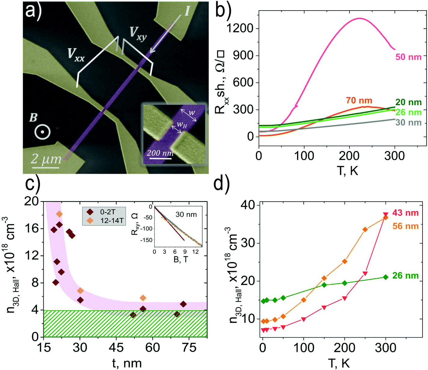 | ||
| Fig. 1 (a) Coloured SEM image (electrodes in yellow and Bi2Se3 nanoribbon in violet) of an individual Bi2Se3 nanoribbon with 6 contacts enabling measurements of the longitudinal (Vxx) and transverse (Vxy) voltages. (b) Temperature dependence of the longitudinal sheet resistance of Bi2Se3 nanoribbons with different thicknesses. (c) Calculated 3D carrier density extracted from the Hall effect in the magnetic field range of 0–2 T (red diamonds) as a function of the nanoribbon thickness; the orange diamonds represent n3D,H extracted at high magnetic fields (12–14 T); T = 2 K. The inset shows the magnetic field dependence of the transverse resistance Rxy for a nanoribbon with t = 30 nm (red solid and orange dashed curves represent linear fits to magnetic field ranges of 0–2 T and 12–14 T). The pink shaded region is a guide to the eye and the green striped region indicates the upper bound for the bulk carrier concentration. (d) Temperature dependence of the 3D carrier density n3D,H extracted from the Hall effect in the magnetic field range of 0–2 T for nanoribbons with different thicknesses. | ||
Fig. 1b shows the temperature dependence of the nanoribbon sheet resistance calculated as Rxx,sh = Rxx × w/L, where L is the distance between the longitudinal contacts. Nanoribbons with thicknesses above 30 nm show a pronounced hump of the Rxx,sh with a maximum at around 220 K. Below this temperature, the resistance decreases with the temperature reaching a saturation at about 2–10 K. We have previously observed a similar behaviour on both Bi2Se3 and Bi2Te3 nanoribbons.24 The presence of a hump in the Rxx,sh(T) can indicate a multiband transport.20,26
The thickness dependence of the n3D,H shown in Fig. 1c is calculated (using eqn (1)) from the Rxy(B) slope at 0–2 T at T = 2 K, for nanoribbons of different thicknesses; data points related to the n3D,H extracted at higher fields of 12–14 T are also reported for three nanoribbons with thicknesses covering the entire explored thickness range. The two values differ by less than 20%, which indicates that the main features of the n3D,Hvs. thickness dependence are not affected by the range of the magnetic field used to fit the Hall resistance.
A striking feature of the dependence shown in Fig. 1c is that the n3D,H increases with the decrease in the nanoribbon thickness. A similar dependence has been reported for thin films of Bi2Se326 and is attributed to the increased density of Se vacancies for thinner films. In the case of an increased Se concentration, for reduced thicknesses, one would expect a higher bulk doping for thinned nanoribbons which should be observed in the entire temperature range. However, as shown in Fig. 1d, at room temperature, the n3D,H for thinner wires is much lower than the value for thicker ones, which rules out variable Se doping at the origin of the peculiar n3D,H (t) shown in Fig. 1c. Moreover, in our case, the data in Fig. 1c are from the same synthesis batch that gives nanoribbons with different thicknesses. We therefore expect to have the same bulk doping for all thicknesses, which furthermore rules out Se vacancies as a possible cause of the n3D,H (t) dependence. The increase of the n3D,H for t < 30 nm is instead indicative of a stronger contribution of surface carriers. In a scenario where surface carriers are formed, with an electron density larger than that of the bulk, reducing the nanoribbon thickness increases the effective carrier density since the bulk contribution becomes less dominant. (Additional effects due to band-bending will be discussed below.)
To confirm this picture, we used additional independent measurements to determine the carrier densities of the bulk, nB, and those of the surface states (topological and/or trivial). In what follows we will indicate the 2D carrier density at the nanoribbon top surface (which interfaces with the vacuum), as nTS, and that at the bottom in contact with the substrate as nInt. To determine the various carrier concentrations, we measure the longitudinal Rxx and transversal Rxy magnetoresistance. We first consider thin nanoribbons (t ≤ 30 nm) where we assume a negligible bulk carrier contribution. Fig. 2a shows the Rxx as a function of the magnetic field for a 30 nm Bi2Se3 nanoribbon (device B13-E5). We observe typical Shubnikov–de Haas (SdH) oscillations. The frequency F of the oscillations is given by the Onsager relationship:
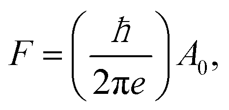 | (2) |
 | ||
| Fig. 2 (a) Shubnikov–de Haas oscillations for a Bi2Se3 nanoribbon (device B13-E5). The inset shows the FFT spectrum of ΔRxx. A single dominating peak is observed at a frequency F = 99 T. An additional peak might be present at lower frequency; however, the signal to noise ratio is too low to draw firm conclusions. (b) Longitudinal and transverse conductance versus magnetic field. The dashed lines correspond to the fit of the two-carrier model. | ||
The angular dependence measured for this thin Bi2Se3 nanoribbon shows a typical F ∼ 1/cos(θ) dependence, where θ is the angle between the magnetic field direction and the surface of the nanoribbon. This confirms the 2D nature of the SdH oscillations (see the ESI, Fig. S4†) and allows us to conclude that the observed SdH oscillations in nanoribbons with t ≤ 30 nm originate from a single surface. We assign these Dirac surface states (DSS) to the top surface (at the interface with vacuum) of the nanoribbon. This is because the SdH oscillations, for all nanoribbons, are not affected by a gate voltage while the Hall conductance can be tuned by a bottom gate (ESI, Fig. S9†). We also exclude that the DSS at the bottom interface (in contact with the substrate) would contribute to the frequency F that we extracted from the SdH oscillations, since this would lead to a modulation of F by an applied gate voltage. The fact that the DSS at the bottom surface do not generate SdH oscillations up to 14 T could be related to its overlapping with the charge accumulation layer formed at the interface with the substrate, as we will discuss below.
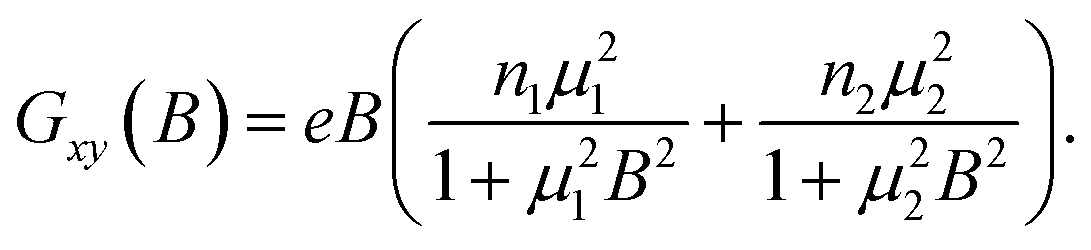
The values of the 2D carrier densities extracted from the SdH oscillations and from the Hall effect measurements show a remarkable discrepancy. For example, for nanoribbon B13-E5 (t = 30 nm) the n2D,SdH is 2.4 × 1012 cm−2 while the n2D,H, calculated as n3D,H× t, is 1.7 × 1013 cm−2, almost an order of magnitude higher. The change of the slope in the transversal resistance data vs. the magnetic field shown in the inset of Fig. 1c is an indication of a contribution of a second band to the total carrier concentration. To extract the carrier concentration and the mobility of the second band (we neglect the bulk), we performed a two-carrier analysis of the longitudinal and transversal magnetoconductance measurements. The conductance tensor in the two-carrier analysis is described as:28
 | (3) |
 | (4) |
 | (5) |
![[thin space (1/6-em)]](https://www.rsc.org/images/entities/char_2009.gif) 600 cm2(Vs)−1, respectively. We assign the n1, extracted from the two-carrier model, to a carrier density deriving from the accumulation layer at the bottom surface; we assume therefore that n1 = nInt. The n1 we extract from fitting (eqn (3) and (4)) is only slightly lower than the experimental n2D,H = 1.7 × 1013 cm−2 indicating that the accumulation layer dominates the Hall conductance. The discrepancy between μ2 extracted from SdH and the value obtained by the two-carrier analysis is most probably due to the different scattering times involved in Hall and SdH measurements.29,30
600 cm2(Vs)−1, respectively. We assign the n1, extracted from the two-carrier model, to a carrier density deriving from the accumulation layer at the bottom surface; we assume therefore that n1 = nInt. The n1 we extract from fitting (eqn (3) and (4)) is only slightly lower than the experimental n2D,H = 1.7 × 1013 cm−2 indicating that the accumulation layer dominates the Hall conductance. The discrepancy between μ2 extracted from SdH and the value obtained by the two-carrier analysis is most probably due to the different scattering times involved in Hall and SdH measurements.29,30
In our two-carrier analysis, we considered that the DSS at the bottom surface has a carrier mobility similar to that of the trivial accumulation layer allowing us to describe both bands by a single carrier concentration nInt. This assumption accounts for: (a) the very good fitting of the conductance tensors without the addition of a third band and (b) the fact that the DSS at the bottom have a much lower mobility. Indeed, in the case of comparable mobility between the DSS at the top and bottom surfaces, one would expect to detect clear signatures in the SdH oscillation that we do not observe. Finally, the relatively lower mobility of the carrier bands at the interface with the substrate (accumulation layer plus DSS having similar mobilities) makes the condition μB ≫ 1, to observe quantum oscillation, unfulfilled at the fields used in our experiment (up to 14 T). The low carrier mobility of the carrier band at the interface with the substrate could possibly be related to an increased electron–electron scattering due to the larger carrier concentration compared to the top surface.
The Hall conductance gives n3D,H = 4 × 1018 cm−3 for thicknesses t > 40 nm (see Fig. 1c). We can therefore consider this value as the upper limit for the hypothetical bulk carrier concentration nB (that we have neglected until now) of the thin nanoribbons. The Fermi energy for these hypothetical bulk electrons, measured from the bottom of the conduction band, can be calculated as31EBF = ℏ2/(2m*)(3π2n3D,Bulk)2/3. Assuming that the effective mass of Bi2Se3 bulk carriers is 0.15 me,32 the EBF is 60 meV. From the SdH oscillations one can extract the Fermi energy of the top surface ETSF measured from the Dirac node: ETSF = ħkFvF, where kF is obtained from eqn (2) and vF is considered to be equal to 5 × 10⁵ m s−1.33,34 Based on this analysis, the ETSF is located in the bulk gap or at the minimum of the conduction band (see Table 1) demonstrating the effectiveness of our catalyst-free PVD method to grow nanoribbons with low residual doping. Taking into account that the Dirac point is about 180 meV below the bottom of the conduction band, one gets a bending of the minimum of the conduction band between the bulk and the top surfaces ΔEBBTS = EBF − (ETSF − 180 meV).34,35
| Nr | t (nm) | n TS (cm−2) | n Int (cm−2) | n B (cm−3) | E TSF (meV) | E BF (meV) | ΔETSBB (meV) | ΔEIntBBa (meV) |
|---|---|---|---|---|---|---|---|---|
| a The band-bending energy at the interface with the substrate ΔEIntBB is calculated as ΔEIntBB = EBF − CBM(0), where the conduction band minimum at the interface with the substrate is extracted from the simulated band-bending diagrams (ESI, Fig. S10). b Calculated as nInt = n2D,H − nTS. c Determined from two-carrier analysis. | ||||||||
| B13-E3 | 26 | 2.1 × 10¹² | 3.8 × 10¹³b | 4 × 10¹⁸ | 170 | 60 | 71 | −280 |
| B13-C3 | 21 | 2.2 × 10¹² | 1.9 × 10¹³b | 172 | 68 | −130 | ||
| B13-E5 | 30 | 2.4 × 10¹² | 1.5 × 10¹³c | 180 | 61 | −40 | ||
| BR3-10R2 | 63 | 2.5 × 10¹² | — | 1.7 × 10¹⁸ | 185 | 35 | 29 | — |
| B21-B1 | 59 | 2.6 × 10¹² | 3.4 × 10¹³ | 2.2 × 10¹⁸ | 187 | 41 | 34 | −200 |
In Table 1 we list the calculated ΔETSBB energies for several Bi2Se3 nanoribbons. For all nanoribbons thinner than 30 nm, the determined BB energy between the DSS and the hypothetical bulk is ΔETSBB ≈ +65 meV indicating an upward band-bending associated with a depletion layer with the depth zTop. To confirm this picture and to evaluate the extension of the depletion zTop and accumulation zInt layers at the two interfaces, we performed self-consistent simulations of the band-bending as discussed in the Methods section using the boundary conditions taken from the experiment. Fig. 3a shows the evolution of the conduction band minimum (CBM) as a function of the distance from the substrate for 5 different nanoribbon thicknesses. In the plot, the Fermi level is at zero energy. The values of zTop and zInt are comparable and on the order of 15 nm; this implies that for nanoribbons less than 30 nm in thickness, the carrier density is determined primarily by the surfaces instead of the bulk. We quantified this assessment by calculating the effective carrier concentration as a function of the nanoribbon thickness, as shown in Fig. 3c. The results show the same qualitative behaviour as the experimental data of Fig. 1c.
 | ||
| Fig. 3 (a) Calculated CBM as a function of the distance from the substrate for nanoribbons of different thicknesses. (b) 3D Schematics: on the left – the band-bending for a 30 nm nanoribbon; on the right – 25 and 60 nm thick nanoribbons and (c) calculated effective carrier density from the self-consistent band-bending of panel a, using a dielectric constant ε = 100. | ||
It is worth pointing out that in the explored range of widths, between 100 and 400 nm, we do not observe a clear width dependence, which is somehow expected. Indeed, the width values of the nanoribbons are in general a factor of 2–20 larger than the thickness. The effective band structure is therefore mostly dominated by the top surface states, the bulk, and the bottom surface states. The effects of confinements due to the width can appear at reduced values comparable to the thickness, a regime we have not explored because of the absence of nanoribbons with widths below 50 nm. Moreover, the carrier concentration density of the 2D gas formed at the interface with the substrate can in general vary from one nanoribbon to the other. These variations are not under control which makes it difficult to observe a possible width dependence.
To experimentally probe the bulk carriers in thick nanoribbons, we measured the Hall conductance and SdH oscillations of nanoribbons with thicknesses above 30 nm. The Rxx as a function of 1/B clearly shows a multifrequency pattern. In Fig. 4a, the SdH oscillations of a nanoribbon with a thickness of 63 nm (device BR3-10R2) are shown at two different gate voltages. As can be seen, the FFT spectra of the Rxx with subtracted background gives two dominating frequencies F1 = 45 T and F2 = 105 T, the latter being very close to the single-frequency SdH oscillation observed in the thin nanoribbons (Fig. 2a, inset and ESI Fig. S1†). At large gate voltages, the charge carriers from the interface states can be tuned and the SdH oscillation frequency, corresponding to these carriers, should change with the applied gate voltage.36 Applying –75 V to the bottom gate shows no change in the frequencies F1 and F2, indicating that F1 and F2 represent either the bulk or the DSS carriers at the top surface. These measurements further confirm that the interface carriers do not show up in the SdH oscillations, while contributing to the Hall conductance.
 | ||
| Fig. 4 (a) Shubnikov–de Haas oscillations of a Bi2Se3 nanoribbon with a thickness of 63 nm at 0 and – 75 V back gate voltages and (b) FFT spectra of SdH oscillations of (a) with removed background ΔRxx. (c) ΔRxxversus 1/B cos(θ) for various angles θ between the magnetic field and the surface normal. The red line is a guide to the eye showing the departure from the 1/B cos(θ) scaling of the SdH oscillations. | ||
The 3D carrier density for the thick nanoribbons can be estimated from the relationship n3D,SdH = 1/(2π)2(4/3) kF3, where kF is the Fermi wave vector extracted from eqn (2). The estimated n3D,SdH for the frequencies F1 and F2 are 1.7 × 10¹⁸ and 6.1 × 1018 cm−3, respectively. F2 gives a carrier density above what we have identified as being the upper limit of a bulk carrier density of 4 × 1018 cm−3 and, for this reason, it cannot be related to the bulk. We therefore associate F1 with the bulk and F2 with the DSS at the top surface.
For thick nanoribbons, the angular dependence of the magnetoresistance Rxx, which is used to map the Fermi surface, should indicate a 3D behaviour i.e. a deviation from the 1/cos(θ) dependence. Fig. 4c illustrates the angular dependence of the SdH oscillations for a 60 nm nanoribbon. The oscillatory part ΔRxx is plotted as a function of 1/B cos(θ). The oscillations are expected to align if they follow the 1/cos(θ) dependence. As one can see, a clear deviation is instead detected for angles θ > 40° (see ESI S6† for the detailed extraction of the 1/cos(θ) dependence).
With the attribution of F1 to the bulk, we can calculate the corresponding bulk density nB. The values we obtain for nanoribbons BR3-10R2 and B21-B1 (t = 63 and 59 nm) are on the order of 2 × 1018 cm−3 which is in good agreement with the value 4 × 1018 cm−3 that we have assumed as the upper limit for the bulk contribution in thin nanoribbons. The interface carrier density nInt for the thick nanoribbons, with multi-frequency SdH oscillations, can be calculated from the total carrier density as nInt = n2D,H − (nB × t + nTS). The value nInt = 3.4 × 1013 cm−2 is similar to the previous value derived from the two-carrier analysis of the thin nanoribbons. The overall results of magnetotransport in thick nanoribbons confirm the high reproducibility of the properties of the DSS and interface states in our Bi2Se3 nanostructures.
It is also worth pointing out that the temperature dependence of the n3D,H shown in Fig. 1d cannot be attributed to the temperature dependence of bulk carriers. Indeed by assuming a temperature independent band bending, the overall n3D should remain rather constant for a Fermi energy of 60 meV (Table 1) in the bulk conduction band. The temperature dependence of the n3D,H can instead be attributed to an interface accumulation layer carrier concentration that depends on the temperature, which itself can also depend on the nanobelt thickness. Such a dependence is not surprising since a similar behavior has been observed in 2DEG gases at LAO/STO interfaces and appear to be a general property of interfaces between two oxide materials.37 The physical origin of the accumulation layer at the interface with the substrate is possibly connected to the interface between the oxide layer surrounding the stoichiometric Bi2Se3 nanoribbons and the SiO2/Si substrate (ESI, Fig. S12†). It is well established that oxide interfaces may exhibit novel properties that are not found in the constituent materials.38,39 A striking example is the LAO/STO interface.37 In high-k/SiO2 interfaces, for example, oxygen displacement at the interface is considered to be responsible for the formation of an interface dipole with an orientation depending on the areal density difference of oxygen atoms at the interface.40 Depending on the sign of the dipole electrons, an accumulation layer can be formed at the interface between the oxides to compensate for the dipole electric field. In our case, the oxide surrounding the nanoribbon and SiO2 are mainly amorphous, with some polycrystalline grains which could be associated with Bi2O3 and SeO2, coupled through van der Waals forces to the substrate (the nanoribbons are mechanically transferred to the substrate) (ESI, Fig. S12†). Only detailed atomistic calculations could therefore possibly give a clear insight into the effective species displacements at the interface accompanied by an electron density redistribution, leading to the formation of a 2DEG. In our specific case, the trivial 2D electron gas, at the interface with the Si02/Si substrate, has a carrier density one order of magnitude higher than the Dirac surface electrons located at the top surface of the nanoribbon. This fact somehow obscures the visibility of the Dirac electrons at the bottom surface of the nanoribbon, affecting the gate response of the devices. For TI thin films instead, the oxide layer is eventually formed only on the top surface, while at the interface with the substrate, one finds the usual surface states characterized by Dirac electrons. This crucial difference makes the transport properties of TI thin films and in general of exfoliated flakes quite different from those of the as-grown nanoribbons.
Finally, it is worth pointing out that the accumulation layer at the substrate interface can be removed by suspending the nanoribbons or by using different substrates and/or properly engineered buffer layers.21
The presence of a depletion layer at the top surface (interfacing the vacuum) is a peculiarity of the PVD technique that was used to grow the nanoribbons. This is also demonstrated in other reports using a similar growth process,34 and contrasts with the finding of accumulation layers formed at the top surface of single crystals,32,41 and MBE thin films.28,42,43
At the same time, signatures of a DSS at the bottom interface, when an in-plane magnetic field aligned with the nanoribbon axis is applied to the sample, have been also detected in magnetotransport. In these measurements, for thin nanoribbons, we clearly see Aharonov–Bohm oscillations associated with orbits around the cross-section (see ESI, Fig. S11†). This indicates that despite the lower mobility of the bottom DSS, coherent trajectories are established on all 4 surfaces of the nanoribbon.
To conclude, our results highlight the promise of controlling the properties of TI materials through growth techniques and dimensionality and establish TI nanoribbons as a viable platform to study new phenomena and effects deriving from the topological protection of the surface states. Furthermore, it shows that post-growth treatment is not necessary to achieve bulk-free transport, significantly simplifying and lowering the requirements for eventual applications of these nanomaterials.
Methods
Transport measurements were performed in a Physical Property Measurement System (PPMS) from Quantum Design, equipped with a 14 T magnet, at a base temperature of 2 K.
Modelling details. We solve self-consistently Poisson's equation for the electrostatic potential V:
| ∇2V(z) = e[n3D(z) + nTSS(z) + Nd]/ε, |
Solving Poisson's equation requires two boundary conditions, which we chose based on the input from the experimental measurements. We set them by fixing V(z) at the two ends of the simulation cell. For the simulations shown in Fig. 3a we impose the condition that the CBM is 300 meV below the EF at z = 0 and 10 meV above the EF at z = t. The resulting average electronic charge density from these simulations,  , is shown in Fig. 3c as a function of t. For the simulations shown in ESI Fig. S10† we choose V(0) such that the electronic charge density integrated from 0 to t – 3 nm,
  , is within 1% of the value of nInt shown in Table 1 while at the top surface we impose the condition that the energy of the Dirac point equals the value of ETSF shown in Table 1.
Disclaimer
The views, opinions and/or findings expressed are those of the author and should not be interpreted as representing the official views or policies of the Department of Defense or the U.S. Government.Conflicts of interest
There are no conflicts to declare.Acknowledgements
The work has been supported by the Knut and Alice Wallenberg Foundation under the project “Dirac Materials”. We also are grateful for support from the European Union for the NANOCOHYBRI project (Cost Action CA 16218) and for the project 766714 – HiTIMe. GK has been partially financed by the Swedish Institute under the Visby project and the ERDF project 1.1.1.2/16/I/001, application No 1.1.1.2/VIAA/1/16/198. The support from the Swedish Infrastructure for Micro- and Nanofabrication-Myfab is acknowledged. The authors would like to thank Krisjanis Smits for help with the HR-TEM images. This research was developed with funding from the Defense Advanced Research Projects Agency (DARPA).References
- L. Fu and C. L. Kane, Phys. Rev. Lett., 2008, 100, 96407 CrossRef PubMed.
- M. Z. Hasan and C. L. Kane, Rev. Mod. Phys., 2010, 82, 3045–3067 CrossRef CAS.
- D. Pesin and A. H. MacDonald, Nat. Mater., 2012, 11, 409–416 CrossRef CAS PubMed.
- A. R. Mellnik, J. S. Lee, A. Richardella, J. L. Grab, P. J. Mintun, M. H. Fischer, A. Vaezi, A. Manchon, E.-A. Kim, N. Samarth and D. C. Ralph, Nature, 2014, 511, 449–451 CrossRef CAS PubMed.
- Y. Shiomi, K. Nomura, Y. Kajiwara, K. Eto, M. Novak, K. Segawa, Y. Ando and E. Saitoh, Phys. Rev. Lett., 2014, 19660 Search PubMed.
- S. Charpentier, L. Galletti, G. Kunakova, R. Arpaia, Y. Song, R. Baghdadi, S. M. Wang, A. Kalaboukhov, E. Olsson, F. Tafuri, D. Golubev, J. Linder, T. Bauch and F. Lombardi, Nat. Commun., 2017, 8, 6–13 CrossRef PubMed.
- H. Peng, K. Lai, D. Kong, S. Meister, Y. Chen, X.-L. Qi, S.-C. Zhang, Z.-X. Shen and Y. Cui, Nat. Mater., 2010, 9, 225–229 CrossRef CAS PubMed.
- F. Xiu, L. He, Y. Wang, L. Cheng, L.-T. Chang, M. Lang, G. Huang, X. Kou, Y. Zhou, X. Jiang, Z. Chen, J. Zou, A. Shailos and K. L. Wang, Nat. Nanotechnol., 2011, 6, 216–221 CrossRef CAS PubMed.
- S. S. Hong, Y. Zhang, J. J. Cha, X. L. Qi and Y. Cui, Nano Latt., 2014, 14, 2815–2821 CrossRef CAS PubMed.
- S. Cho, B. Dellabetta, R. Zhong, J. Schneeloch, T. Liu, G. Gu, M. J. Gilbert and N. Mason, Nat. Commun., 2015, 6, 7634 CrossRef PubMed.
- L. A. Jauregui, M. T. Pettes, L. P. Rokhinson, L. Shi and Y. P. Chen, Nat. Nanotechnol., 2016, 11, 345–351 CrossRef CAS PubMed.
- I. Appelbaum, H. D. Drew and M. S. Fuhrer, Appl. Phys. Lett., 2011, 98, 023103 CrossRef.
- J. Tian, S. Hong, I. Miotkowski, S. Datta and Y. P. Chen, Sci. Adv., 2017, 3, e1602531 CrossRef PubMed.
- A. Cook and M. Franz, Phys. Rev. B – Rapid Commun., 2011, 84, 201105 CrossRef.
- A. M. Cook, M. M. Vazifeh and M. Franz, Phys. Rev. B: Condens. Matter Mater. Phys., 2012, 86, 155431–155417 CrossRef.
- F. de Juan, R. Ilan and J. H. Bardarson, Phys. Rev. Lett., 2014, 113, 107003 CrossRef PubMed.
- R. Ilan, J. H. Bardarson, H. S. Sim and J. E. Moore, New J. Phys., 2014, 16, 53007–53013 CrossRef.
- J. Manousakis, A. Altland, D. Bagrets, R. Egger and Y. Ando, Phys. Rev. B, 2017, 95, 165424 CrossRef.
- L. Xue, P. Zhou, C. X. Zhang, C. Y. He, G. L. Hao, L. Z. Sun and J. X. Zhong, AIP Adv., 2013, 3, 52105 CrossRef.
- Y. Xu, I. Miotkowski, C. Liu, J. Tian, H. Nam, N. Alidoust, J. Hu, C.-K. Shih, M. Z. Hasan and Y. P. Chen, Nat. Phys., 2014, 10, 956–963 Search PubMed.
- N. Koirala, M. Brahlek, M. Salehi, L. Wu, J. Dai, J. Waugh, T. Nummy, M. G. Han, J. Moon, Y. Zhu, D. Dessau, W. Wu, N. P. Armitage and S. Oh, Nano Lett., 2015, 15, 8245–8249 CrossRef CAS PubMed.
- J. Moon, N. Koirala, M. Salehi, W. Zhang, W. Wu and S. Oh, Nano Lett., 2018, 820–826 CrossRef CAS PubMed.
- S. S. Hong, J. J. Cha, D. Kong and Y. Cui, Nat. Commun., 2012, 3, 757 CrossRef PubMed.
- J. Andzane, G. Kunakova, S. Charpentier, V. Hrkac, L. Kienle, M. Baitimirova, T. Bauch, F. Lombardi and D. Erts, Nanoscale, 2015, 7, 15935 RSC.
- K. Storm, F. Halvardsson, M. Heurlin, D. Lindgren, A. Gustafsson, P. M. Wu, B. Monemar and L. Samuelson, Nat. Nanotechnol., 2012, 7, 718–722 CrossRef CAS PubMed.
- Y. S. Kim, M. Brahlek, N. Bansal, E. Edrey, G. A. Kapilevich, K. Iida, M. Tanimura, Y. Horibe, S.-W. Cheong and S. Oh, Phys. Rev. B: Condens. Matter Mater. Phys., 2011, 84, 73109 CrossRef.
- Y. Ando, J. Phys. Soc. Jpn., 2013, 82, 102001–102032 CrossRef.
- N. Bansal, Y. S. Kim, M. Brahlek, E. Edrey and S. Oh, Phys. Rev. Lett., 2012, 109, 116804 CrossRef PubMed.
- Z. Ren, A. Taskin, S. Sasaki, K. Segawa and Y. Ando, Phys. Rev. B: Condens. Matter Mater. Phys., 2010, 82, 241306 CrossRef.
- K. Eto, Z. Ren, A. Taskin, K. Segawa and Y. Ando, Phys. Rev. B: Condens. Matter Mater. Phys., 2010, 81, 195309 CrossRef.
- M. Brahlek, N. Koirala, N. Bansal and S. Oh, Solid State Commun., 2015, 215, 54–62 CrossRef.
- J. G. Analytis, J.-H. Chu, Y. Chen, F. Corredor, R. D. McDonald, Z. X. Shen and I. R. Fisher, Phys. Rev. B: Condens. Matter Mater. Phys., 2010, 81, 205407 CrossRef.
- H. Zhang, C.-X. Liu, X.-L. Qi, X. Dai, Z. Fang and S.-C. Zhang, Nat. Phys., 2009, 5, 438–442 Search PubMed.
- Y. Xia, D. Qian, D. Hsieh, L. Wray, A. Pal, H. Lin, A. Bansil, D. Grauer, Y. S. Hor, R. J. Cava and M. Z. Hasan, Nat. Phys., 2009, 5, 398–402 Search PubMed.
- L. Veyrat, F. Iacovella, J. Dufouleur, C. Nowka, H. Funke, M. Yang, W. Escoffier, M. Goiran, B. Eichler, O. G. Schmidt, B. Büchner, S. Hampel and R. Giraud, Nano Lett., 2015, 15, 7503–7507 CrossRef CAS PubMed.
- B. Sacépé, J. B. Oostinga, J. Li, A. Ubaldini, N. J. G. Couto, E. Giannini and A. F. Morpurgo, Nat. Commun., 2011, 2, 575 CrossRef PubMed.
- M. Huijben, G. Koster, M. K. Kruize, S. Wenderich, J. Verbeeck, S. Bals, E. Slooten, B. Shi, H. J. A. Molegraaf, J. E. Kleibeuker, S. Van Aert, J. B. Goedkoop, A. Brinkman, D. H. A. Blank, M. S. Golden, G. Van Tendeloo, H. Hilgenkamp and G. Rijnders, Adv. Funct. Mater., 2013, 23, 5240–5248 CrossRef CAS.
- J. W. Park, D. F. Bogorin, C. Cen, D. A. Felker, Y. Zhang, C. T. Nelson, C. W. Bark, C. M. Folkman, X. Q. Pan, M. S. Rzchowski, J. Levy and C. B. Eom, Nat. Commun., 2010, 1, 94 CrossRef CAS PubMed.
- H. Y. Hwang, Y. Iwasa, M. Kawasaki, B. Keimer, N. Nagaosa and Y. Tokura, Nat. Mater., 2012, 11, 103–113 CrossRef CAS PubMed.
- K. Kita and A. Toriumi, Appl. Phys. Lett., 2009, 132902 CrossRef.
- M. Bianchi, D. Guan, S. Bao, J. Mi, B. B. Iversen, P. D. C. King and P. Hofmann, Nat. Commun., 2010, 1, 125–128 CrossRef PubMed.
- M. Brahlek, Y. S. Kim, N. Bansal, E. Edrey and S. Oh, Appl. Phys. Lett., 2011, 99, 10–13 CrossRef.
- M. Brahlek, N. Koirala, M. Salehi, N. Bansal and S. Oh, Phys. Rev. Lett., 2014, 113, 1–5 CrossRef PubMed.
- N. P. Butch, K. Kirshenbaum, P. Syers, A. B. Sushkov, G. S. Jenkins, H. D. Drew and J. Paglione, Phys. Rev. B: Condens. Matter Mater. Phys., 2010, 81, 241301 CrossRef.
Footnotes |
| † Electronic supplementary information (ESI) available. See DOI: 10.1039/c8nr05500a |
| ‡ “Sandia National Laboratories is a multimission laboratory managed and operated by National Technology and Engineering Solutions of Sandia, LLC., a wholly owned subsidiary of Honeywell International, Inc., for the US Department of Energy's National Nuclear Security Administration under Contract No. DE-NA-0003525.” |
| This journal is © The Royal Society of Chemistry 2018 |