
 Open Access Article
 This Open Access Article is licensed under a Creative Commons Attribution-Non Commercial 3.0 Unported Licence
Optically controlled dielectric properties of single-walled carbon nanotubes for terahertz wave applications†
Serguei
Smirnov
 a,
Ilya V.
Anoshkin
ab,
Petr
Demchenko
b,
Daniel
Gomon
b,
Dmitri V.
Lioubtchenko
*ab,
Mikhail
Khodzitsky
b and
Joachim
Oberhammer
a
a,
Ilya V.
Anoshkin
ab,
Petr
Demchenko
b,
Daniel
Gomon
b,
Dmitri V.
Lioubtchenko
*ab,
Mikhail
Khodzitsky
b and
Joachim
Oberhammer
a
aDepartment of Micro and Nanosystems, KTH Royal Institute of Technology, Osquldas väg 10, SE-100 44, Stockholm, Sweden. E-mail: dml@kth.se
bDepartment of Photonics and Optical Information Technologies, ITMO University, 49 Kronverkskiy pr., 197101, Saint Petersburg, Russian Federation
First published on 12th June 2018
Abstract
Materials with tunable dielectric properties are valuable for a wide range of electronic devices, but are often lossy at terahertz frequencies. Here we experimentally report the tuning of the dielectric properties of single-walled carbon nanotubes under light illumination. The effect is demonstrated by measurements of impedance variations at low frequency as well as complex dielectric constant variations in the wide frequency range of 0.1–1 THz by time domain spectroscopy. We show that the dielectric constant is significantly modified for varying light intensities. The effect is also practically applied to phase shifters based on dielectric rod waveguides, loaded with carbon nanotube layers. The carbon nanotubes are used as tunable impedance surface controlled by light illumination, in the frequency range of 75–500 GHz. These results suggest that the effect of dielectric constant tuning with light, accompanied by low transmission losses of the carbon nanotube layer in such an ultra-wide band, may open up new directions for the design and fabrication of novel Terahertz and optoelectronic devices.
Introduction
Terahertz (THz) technologies meet nowadays an expanding academic and industrial interest.1 The design of basic components in the frequency range of 0.1–1.0 THz is relevant for a wide range of applications, such as telecommunications, radar and imaging systems, material spectroscopy, and medical imaging and diagnosis.2–6 With that development in mind, dielectric waveguides and in particular dielectric rod waveguides (DRWs) are one of the prospective platforms for THz electronics.7 Notably, designed and fabricated phase shifters, amplifiers, active and passive antennas, and electrically controllable attenuators have already been demonstrated.8–12 Dielectric waveguides offer a considerable reduction of the propagation losses in comparison to standard metal waveguides.13,14 Another noteworthy property of the DRWs is that semiconductor devices such as Gunn or Impatt diodes, mixers and detectors, modulators, and oscillators, can be fabricated in situ on the semiconducting waveguide.15,16 Furthermore, dielectric waveguides do not have a cut-off frequency, enabling ultra-wide band operation.17 The DRW is an open, i.e., not metal-shielded, waveguide system that can be affected with external electro-magnetic fields including light. Consequently, by covering a wall of the waveguide with a variable impedance layer, the propagation constant can be dynamically tuned.9 One of the first applications of optically controlled phase-shifters based on a generated plasma layer in silicon DRWs was reported by Lee et al.18Materials with electrically and/or optically tunable properties, such as high impedance surfaces, are thus relevant for a number of applications like phase shifters, attenuators, and steerable antennas.19,20 However, existing materials with tunable impedance are usually very lossy at the millimeter-wave and THz frequencies.21 Therefore, novel nanomaterials and metamaterials are extensively studied, and have been shown to display attractive electronic and optoelectronic properties.22 For instance, single-walled carbon nanotube (SWCNT) layers were used for optically-controlled phase shifters.23,24 The simplicity of the SWCNTs deposition on a wide range of substrates is suitable for large surface area devices, e.g. for the fabrication of reflector surface coatings, absorbers, sensor matrices, and antennas.25,26 SWCNT-based components can also be integrated with DRW antenna elements for THz beam steering applications.27 The propagation characteristics of DRWs loaded with SWCNTs on polyethylene terephthalate (PET) substrates were studied theoretically and experimentally.28 The propagation losses were shown to decrease in the range of 75–320 GHz due to rapid decrease of the SWCNT layer's conductivity with the frequency.28 However, the tunability of the dielectric properties of SWCNT in the THz range has not been reported yet, or is limited to DC characterization in the form of photocurrent measurements in response to optical and THz illumination.29,30
In this paper, we experimentally investigate SWCNT layers under light illumination through a wide range of techniques and frequencies, with the aim to integrate them as tunable impedance surfaces for THz applications. The results presented here include: characterization with scanning electron microscopy (SEM), transmission electron microscopy (TEM), optical spectroscopy in the 200–2500 nm wavelength range, and Terahertz time domain spectroscopy (THz TDS) in the 0.2–1 THz frequency range. We also propose a design of optically-controlled THz phase shifters based on SWCNT-loaded DRWs. The devices are characterized by vector network analyzer (VNA) S-parameter measurements in the 75–500 GHz frequency range. Throughout the study, we demonstrate the pertinence of SWCNTs for their integration as tunable impedance surfaces in very broadband THz applications. Thin carbon nanotube layers’ conductivity can be optimized to decrease the induced propagation losses; and light illumination is shown to modify their complex dielectric constant.
Results and discussion
Carbon nanotubes were synthesized by aerosol chemical vapor deposition, with precise control over their morphology, bundle formation, and layer thickness.31 The method of SWCNT production in the aerosol phase allows producing SWCNTs with very high quality.32 The absorbance spectrum of the sample, prepared by dry transfer method onto a quartz substrate (see ESI, Fig. S2†) is shown in Fig. 1a. The carbon nanotube intrinsic peaks are observed: π-plasmon peak (∼260 nm) originating from sp2 hybridized bonds, S11 peak due to the first electron transitions in semiconducting SWCNTs, and M11 peak due to the first transitions in metallic SWCNTs. From these results, the nanotube diameter, density and the thickness of the layer can be estimated according to ref. 33. The SWCNTs diameters of 1.3–2.0 nm were calculated from the S11 peak position according to the Kataura plot.34Fig. 1b and c show respectively a SEM image of the SWCNT network on quartz substrate and a TEM image of the individual nanotubes. Raman spectra of the samples are shown in Fig. S1.† Both high ratio of G/D peak intensities in the Raman spectra, widely used to estimate the quality of SWCNTs, and TEM observations allow supposing that all carbon is incorporated within the SWCNT lattice (see additional discussion of the SWCNT characterization in the ESI†).33,35 SWCNT layers were deposited by press dry transfer from the nitrocellulose filter onto the samples, as illustrated in Fig. S2.† The different samples included quartz substrates with gold contact electrodes, sapphire DRWs, and polytetrafluoroethylene (PTFE) substrates.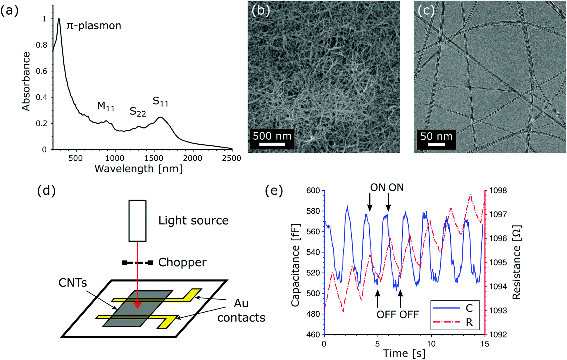 | ||
| Fig. 1 Characterization of thin SWCNT layers: (a) optical absorbance spectrum of the SWCNT sample. The average diameter of the SWCNTs was calculated from the S11 peak positions using the Kataura plot.31 (b) SEM image of the SWCNTs. (c) TEM image of the SWCNTs. (d) Schematic drawing of the parallel-contacts measurement setup of the SWCNT layer on a quartz substrate under light illumination. (e) Measured influence of cyclic illumination on the capacitance and the resistance of the SWCNT layer. | ||
In order to demonstrate the optical tuning of the dielectric constant, we performed a first direct impedance measurement at low frequency. A SWCNT layer was applied on a quartz substrate with dual parallel gold electrodes and illuminated by a laser with a wavelength of 532 nm, as shown in the schematic drawing in Fig. 1d. The measured capacitance and resistance of the sample were both decreasing under cyclic illumination (Fig. 1e). The observed capacitance variation is around 10%, while the resistance variation is under 0.2%. This measurement allows supposing that the dielectric constant tuning is more sensitive to light illumination than the conductivity tuning.
To characterize the optical tuning of the dielectric constant of the SWCNTs in a wide frequency range, we performed terahertz time domain spectroscopy on the samples. THz TDS is a powerful tool actively developed since the 1990s for the measurement of dielectric properties of materials (permittivity, conductivity and permeability). It is based on the generation and the detection of ultra-short pulses by a coherent and time-gated method using near-infrared femtosecond (fs) lasers. The complex dielectric constant of materials can be calculated from the amplitude and phase measurements of the THz pulse's spectral components.36 A schematic diagram of the THz TDS setup is shown in Fig. 2a.37,38 A fs infrared laser pulse was split into two beams with the ratio of 1![[thin space (1/6-em)]](https://www.rsc.org/images/entities/char_2009.gif) :9. The “probe beam” contained 10% of the energy and the “pump beam” – 90%. The generation of the THz signal occurred on an InAs crystal in a magnetic field of 2 T. After passing through an IR filter, the THz beam irradiated the sample. The sample was simultaneously illuminated with a laser in continuous wave mode at a wavelength of 980 nm with optical power varied from 1 mW to 2 W. The illumination area was approximately 4 cm2. The complex conductivity of the SWCNTs (
:9. The “probe beam” contained 10% of the energy and the “pump beam” – 90%. The generation of the THz signal occurred on an InAs crystal in a magnetic field of 2 T. After passing through an IR filter, the THz beam irradiated the sample. The sample was simultaneously illuminated with a laser in continuous wave mode at a wavelength of 980 nm with optical power varied from 1 mW to 2 W. The illumination area was approximately 4 cm2. The complex conductivity of the SWCNTs (![[small sigma, Greek, circumflex]](https://www.rsc.org/images/entities/i_char_e111.gif) CNT) was obtained from the measured transmission data:39
CNT) was obtained from the measured transmission data:39
 | (1) |
![[small epsilon, Greek, circumflex]](https://www.rsc.org/images/entities/i_char_e107.gif) CNT) was then expressed as:40
CNT) was then expressed as:40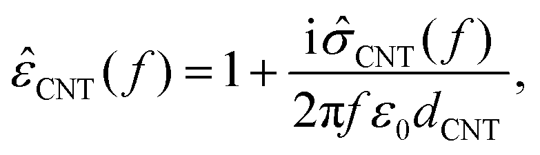 | (2) |
 | ||
| Fig. 2 Characterization of SWCNTs by terahertz time domain spectroscopy: (a) schematic drawing of the THz TDS setup. Ch – optical chopper, InAs – THz generator (InAs crystal in a magnetic field of 2 T), G – Glan prism, CdTe – nonlinear crystal, λ/2 and λ/4 – half-wave and quarter-wave plates, W – Wollaston prism. (b) Variation of the detected THz signal's peak amplitude in the “on” and “off” illumination states. Inset – single THz pulse. (c, d) Real and imaginary parts of the SWCNT sample's dielectric constant, extracted from THz TDS measurements. A significant increase of the real part and a decrease of the imaginary part are observed with increasing light intensities. | ||
Peak amplitudes of the detected THz pulses (see inset of Fig. 2b) were recorded as a function of the sample illumination. An average increase of 8% in the amplitude is observed during illumination, as shown in Fig. 2b. The excitation wavelength here is different from the laser wavelength used for the direct impedance measurements, corresponding to a different optical absorbance value of the SWCNT layer. We thus acknowledge that the comparison is only valid qualitatively. The measured complex dielectric constant of the SWCNTs, calculated from (2), is shown in Fig. 2c and d. Without illumination, the imaginary part of the dielectric constant globally decreases with the frequency, similar to ref. 28. The real part of the dielectric constant is negative below 0.3 THz. Moreover, it exhibits a resonant behavior that suggests that the conductivity cannot be described by the simple Drude model. Instead, one can use a Drude–Lorentz model combined with the Maxwell–Garnett theory.42 Under illumination of the SWCNTs, the real part of the sample's dielectric constant is increasing, while the imaginary part is decreasing, with augmenting light intensities of 0.312, 0.47, and 0.7 W cm−2. We explain the modification of the dielectric constant under illumination by an optically induced polarization of the carbon nanotubes43 and electronic transitions between the Van Hove singularities. To be confirmed, this effect requires further systematic studies of the illumination parameters and the SWCNTs types, such as length, diameter, chirality, and layer thickness. Nevertheless, the currently observed tuning range is significant and we believe the effect will see potential applications in novel terahertz and optoelectronic devices.
We propose a practical implementation of the dielectric constant tuning in optically-controlled THz phase shifters. Thin SWCNT layers were applied onto the wall of dielectric rod waveguides, as shown on the schematic of the experimental setup in Fig. 3a and image in Fig. 3b. The suspended rod tapers were then inserted in two standard metal waveguide ports. Full two-port S-parameter measurements were performed with a vector network analyzer in the 75–500 GHz frequency range.
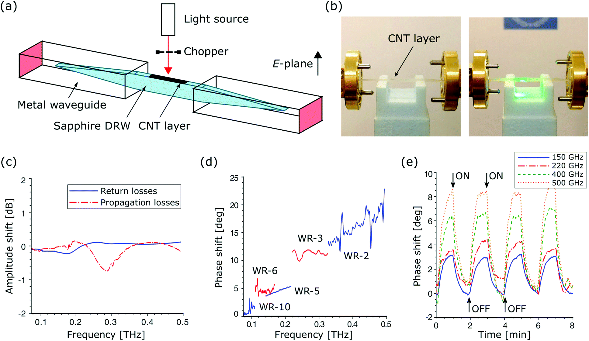 | ||
| Fig. 3 Proposed terahertz phase shifter design based on optically controlled SWCNT layer: (a) schematic drawing of the VNA two-port S-parameter measurement setup. A double-sided symmetrically-tapered DRW is loaded with a SWCNT layer and exposed to varying illumination conditions. (b) Image of the measurement setup. (c) Measured S-parameter amplitude shift due to the illumination of the SWCNT layer. (d) Measured phase shift. (e) Measured influence of cyclic illumination on the phase shift at the discrete frequencies of 150, 220, 400 and 500 GHz. | ||
The results of the VNA measurements are given in Fig. 3. The amplitude shift, induced by light illumination of the SWCNT-loaded DRW, is shown in Fig. 3c. The variation of the return losses and the propagation losses is for both values below 0.8 dB, in the whole measured frequency range. The relative phase shift between the illuminated and the non-illuminated state of the SWCNT layer is given in Fig. 3d. An approximately linear relation between the phase shift and the frequency is observed. The tuning of the dielectric constant of the SWCNT layer, located on a wall of the DRW, induces the change of the propagation constant inside the waveguide. The altered phase velocity over the length of the SWCNT layer provokes a phase shift compared to the non-illuminated state. Meanwhile, the conductivity change is negligible and almost no additional losses due to the nanotubes are detected, confirming the impedance measurements in Fig. 1e. The time dependence of the phase shifting effect was also measured with the VNA setup at several discrete frequencies of 150, 220, 400 and 500 GHz. The SWCNT layer illumination was performed in 2, 4 and 20 minute-long on/off cycles to record the dynamics of the effect. The results of the phase measurements are given in Fig. 3e and additionally in Fig. S3.† Long-term drifts, most probably due to room temperature variations, were subtracted for easier comparison between the measurements. The observed phase increases/decreases when the illumination is respectively activated/deactivated. The amplitude of the phase shift also increases with the frequency, which confirms the optical control of the phase shift.
Conclusions
We have experimentally demonstrated the tuning of the dielectric constant of single-walled carbon nanotubes under light illumination. The effect was illustrated by direct impedance measurements at low frequency as well as complex dielectric constant measurements in the wide frequency range of 0.1–1 THz by means of time domain spectroscopy. We suppose that the dielectric constant is tuned due to the unique optical absorption properties of carbon nanotubes, such as light-induced polarization change. However, further studies with varying illumination parameters and SWCNT samples will be needed to confirm the theory. The effect was also applied for the design of terahertz phase shifters based on dielectric rod waveguides loaded with thin carbon nanotube layers. The phase shifters were shown to work in the frequency range of 75–500 GHz due to the impedance change of the carbon nanotube layer by light illumination. We believe that the effect of complex dielectric constant tuning under light illumination, accompanied by low level of propagation losses of the SWCNT layer in such an ultra-wide band, will open up new approaches for the design and fabrication of novel low-loss and compact terahertz and optoelectronic systems.Experimental details
Experimental details are given in the ESI.†Conflicts of interest
There are no conflicts to declare.Acknowledgements
This work was financially supported in part by the European Union (EU) Horizon 2020 Innovative Training Network CELTA under grant agreement no. 675683 of Call: H2020-MSCA-ITN-2015, by the European Research Council (ERC) under the European Union's Horizon 2020 research and innovation programme (grant agreement no. 616846), by the Government of Russian Federation, Grant 074-U01, and by the ITMO Fellowship and Professorship Program.References
- I. Hosako, N. Sekine, M. Patrashin, S. Saito, K. Fukunaga, Y. Kasai, P. Baron, T. Seta, J. Mendrok, S. Ochiai and H. Yasuda, Proc. IEEE, 2007, 95, 1611–1623 Search PubMed.
- M. Borovkova, M. Serebriakova, V. Fedorov, E. Sedykh, V. Vaks, A. Lichutin, A. Salnikova and M. Khodzitsky, Biomed. Opt. Express, 2017, 8, 273–280 CrossRef PubMed.
- J. El Haddad, B. Bousquet, L. Canioni and P. Mounaix, TrAC, Trends Anal. Chem., 2013, 44, 98–105 CrossRef.
- T. Kleine-Ostmann and T. Nagatsuma, J. Infrared Millim. Terahertz Waves, 2011, 32, 143–171 CrossRef.
- W. Menzel, 2010 European Radar Conf. (EuRAD), Paris, France, 30 Sep.-1 Oct. 2010, pp. 89–92.
- P. H. Siegel, IEEE Trans. Microwave Theory Tech., 2004, 52, 2438–2447 CrossRef.
- D. V. Lioubtchenko, S. N. Dudorov and A. V. Raisanen, 2001 31st European Microwave Conf., London, England, 24–26 Sep. 2001, pp. 1–4.
- M. Koeberle, M. Hoefle, A. Gaebler, A. Penirschke and R. Jakoby, 2011 Int. Conf. Infrared, Millimeter and Terahertz Waves, Houston, TX, USA, 2–7 Oct. 2011, p. 1.
- D. Chicherin, M. Sterner, J. Oberhammer, S. Dudorov, D. Lioubtchenko, A. J. Niskanen, V. Ovchinnikov and A. V. Räisänen, Proc. 40th European Microwave Conf., Paris, France, 28–30 Sep. 2010, pp. 950–953.
- D. V. Lioubtchenko, P. Pousi, S. N. Dudorov, A. V. Raisanen, A. Deleniv, V. Drakinskiy and S. Gevorgian, Proc. 38th European Microwave Conf, Amsterdam, Netherlands, 27–31 Oct. 2008, pp. 1204–1206.
- P. Pousi, D. Lioubtchenko, S. Dudorov and A. V. Raisanen, 2008 38th European Microwave Conf., Amsterdam, Netherlands, 27–31 Oct. 2008, pp. 1082–1085.
- J. P. Pousi, D. V. Lioubtchenko, S. N. Dudorov and A. V. Raisanen, IEEE Trans. Antennas Propag., 2010, 58, 714–719 Search PubMed.
- D. Lioubtchenko, S. Dudorov, J. Mallat, J. Tuovinen and A. V. Raisanen, IEEE Microw. Wirel. Compon. Lett., 2001, 11, 252–254 Search PubMed.
- D. Lioubtchenko, S. Tretyakov and S. Dudorov, Millimeter-wave waveguides, Springer Science & Business Media, New York, 2003 Search PubMed.
- A. A. Generalov, D. V. Lioubtchenko, J. A. Mallat, V. Ovchinnikov and A. V. Raisanen, IEEE Trans. Terahertz Sci. Technol., 2012, 2, 623–628 Search PubMed.
- A. Rivera-Lavado, S. Preu, L. E. García-Muñoz, A. Generalov, J. M. de Paz, G. Döhler, D. Lioubtchenko, M. Méndez-Aller, F. Sedlmeir, M. Schneidereit, H. G. L. Schwefel, S. Malzer, D. Segovia-Vargas and A. V. Räisänen, IEEE Trans. Antennas Propag., 2015, 63, 882–890 Search PubMed.
- A. A. Generalov, D. V. Lioubtchenko and A. V. Räisänen, Proc. 7th European Conf. Antennas and Propagation (EuCAP), Gothenburg, Sweden, 8–12 Apr. 2013, pp. 541–544.
- C. Lee, P. Mak and A. DeFonzo, IEEE J. Quantum Electron., 1980, 16, 277–288 Search PubMed.
- D. Chicherin, S. Dudorov, D. Lioubtchenko, V. Ovchinnikov, S. Tretyakov and A. V. Räisänen, Microw. Opt. Technol. Lett., 2006, 48, 2570–2573 CrossRef.
- D. Chicherin, M. Sterner, D. Lioubtchenko, J. Oberhammer and A. V. Räisänen, Int. J. Microw. Wirel. Technol., 2011, 3, 533–538 CrossRef.
- T. F. Gallacher, R. Sondena, D. A. Robertson and G. M. Smith, IEEE Trans. Microwave Theory Tech., 2012, 60, 2301–2309 Search PubMed.
- D. Jariwala, V. K. Sangwan, L. J. Lauhon, T. J. Marks and M. C. Hersam, Chem. Soc. Rev., 2013, 42, 2824–2860 RSC.
- D. V. Lioubtchenko, I. V. Anoshkin, I. I. Nefedova, J. Oberhammer and A. V. Räisänen, 2017 IEEE MTT-S Int. Microwave Symp. (IMS), Honololu, HI, USA, 4–9 Jun. 2017, pp. 1188–1191.
- D. V. Lioubtchenko, A. Rivera-Lavado, I. I. Nefedova, I. Anoshkin, L. E. García-Muñoz and A. V. Räisänen, Proc. Global Symp. Millimeter Waves (GSMM) ESA Workshop Millimetre-Wave Technology and Applications, Espoo, Finland, 6–8 Jun. 2016, pp. 1–3.
- X.-C. Wang and S. A. Tretyakov, 2017, arXiv preprint arXiv:1712.01708.
- T. F. Gallacher, D. A. Robertson and G. M. Smith, IEEE Trans. Antennas Propag., 2013, 61, 1688–1696 Search PubMed.
- A. Rivera-Lavado, S. Preu, L. E. Garcia-Munoz, A. Generalov, J. M. de Paz, G. Dohler, D. Lioubtchenko, M. Mendez-Aller, S. Malzer, D. Segovia-Vargas and A. V. Raisanen, 2015 European Microwave Conf. (EuMC), Paris, France, 7–10 Sep. 2015, pp. 917–920.
- I. I. Nefedova, D. V. Lioubtchenko, I. S. Nefedov and A. V. Räisänen, IEEE Trans. Terahertz Sci. Technol., 2016, 6, 840–845 Search PubMed.
- J.-L. Zhu, G. Zhang, J. Wei and J.-L. Sun, Appl. Phys. Lett., 2012, 101, 123117 CrossRef.
- Y. Wang, G. Zhang, L. Qiao, J. Wei, J.-L. Zhu, Z. Chen, Z. Zhao and J.-L. Sun, Opt. Express, 2014, 22, 5895–5903 CrossRef PubMed.
- I. V. Anoshkin, A. G. Nasibulin, Y. Tian, B. Liu, H. Jiang and E. I. Kauppinen, Carbon, 2014, 78, 130–136 CrossRef.
- Q. Zhang, N. Wei, P. Laiho and E. I. Kauppinen, Top. Curr. Chem., 2017, 375, 1 CrossRef PubMed.
- I. V. Anoshkin, I. I. Nefedova, D. V. Lioubtchenko, I. S. Nefedov and A. V. Räisänen, Carbon, 2017, 116, 547–552 CrossRef.
- H. Kataura, Y. Kumazawa, Y. Maniwa, I. Umezu, S. Suzuki, Y. Ohtsuka and Y. Achiba, Synth. Met., 1999, 103, 2555–2558 CrossRef.
- I. V. Anoshkin, A. G. Nasibulin, P. R. Mudimela, J. Raula, V. Ermolov and E. I. Kauppinen, Carbon, 2012, 50, 4171–4174 CrossRef.
- X.-C. Zhang and J. Xu, Introduction to THz Wave Photonics, Springer, 2010, vol. 29 Search PubMed.
- V. Y. Soboleva, D. A. Gomon, E. A. Sedykh, V. K. Balya and M. K. Khodzitski, J. Opt. Technol., 2017, 84, 521 CrossRef.
- D. A. Gomon, E. A. Sedykh, S. Rodriguez, I. T. Monroy, K. I. Zaitsev, A. V. Vozianova and M. K. Khodzitsky, Chin. Opt., 2018, 11, 47–59 Search PubMed.
- G. Jnawali, Y. Rao, H. Yan and T. F. Heinz, Nano Lett., 2013, 13, 524–530 CrossRef PubMed.
- C. How Gan, Appl. Phys. Lett., 2012, 101, 111609 CrossRef.
- A. G. Nasibulin, A. Kaskela, K. Mustonen, A. S. Anisimov, V. Ruiz, S. Kivistö, S. Rackauskas, M. Y. Timmermans, M. Pudas, B. Aitchison, M. Kauppinen, D. P. Brown, O. G. Okhotnikov and E. I. Kauppinen, ACS Nano, 2011, 5, 3214–3221 CrossRef PubMed.
- O. Levy and D. Stroud, Phys. Rev. B: Condens. Matter Mater. Phys., 1997, 56, 8035 CrossRef.
- K. Gharbavi and H. Badehian, AIP Adv., 2015, 5, 077155 CrossRef.
Footnote |
| † Electronic supplementary information (ESI) available: Raman spectra of the SWCNT samples (Fig. S1); dry transfer method steps of the SWCNT layer onto a quartz substrate (Fig. S2); time dependence of the phase shift in the SWCNT-loaded DRW with 4 and 20 minutes on/off illumination cycles (Fig. S3). Methods: carbon nanotube sample characterization; THz TDS measurement setup; THz VNA measurement setup. See DOI: 10.1039/c8nr03740j |
| This journal is © The Royal Society of Chemistry 2018 |