
 Open Access Article
 This Open Access Article is licensed under a Creative Commons Attribution-Non Commercial 3.0 Unported Licence
Plasmon response evaluation based on image-derived arbitrary nanostructures†
S.
Trautmann
ab,
M.
Richard-Lacroix
ab,
A.
Dathe
a,
H.
Schneidewind
 a,
J.
Dellith
a,
W.
Fritzsche
a and
V.
Deckert
*ab
a,
J.
Dellith
a,
W.
Fritzsche
a and
V.
Deckert
*ab
aLeibniz Institute of photonic technology (IPHT), Albert-Einstein-Straße 9, D-07745 Jena, Germany. E-mail: volker.deckert@leibniz-ipht.de
bInstitute of Physical Chemistry and Abbe Center of Photonics, University of Jena, Helmholtzweg 4, D-07743 Jena, Germany
First published on 18th May 2018
Abstract
The optical response of realistic 3D plasmonic substrates composed of randomly shaped particles of different size and interparticle distance distributions in addition to nanometer scale surface roughness is intrinsically challenging to simulate due to computational limitations. Here, we present a Finite Element Method (FEM)-based methodology that bridges in-depth theoretical investigations and experimental optical response of plasmonic substrates composed of such silver nanoparticles. Parametrized scanning electron microscopy (SEM) images of surface enhanced Raman spectroscopy (SERS) active substrate and tip-enhanced Raman spectroscopy (TERS) probes are used to simulate the far-and near-field optical response. Far-field calculations are consistent with experimental dark field spectra and charge distribution images reveal for the first time in arbitrary structures the contributions of interparticle hybridized modes such as sub-radiant and super-radiant modes that also locally organize as basic units for Fano resonances. Near-field simulations expose the spatial position-dependent impact of hybridization on field enhancement. Simulations of representative sections of TERS tips are shown to exhibit the same unexpected coupling modes. Near-field simulations suggest that these modes can contribute up to 50% of the amplitude of the plasmon resonance at the tip apex but, interestingly, have a small effect on its frequency in the visible range. The band position is shown to be extremely sensitive to particle nanoscale roughness, highlighting the necessity to preserve detailed information at both the largest and the smallest scales. To the best of our knowledge, no currently available method enables reaching such a detailed description of large scale realistic 3D plasmonic systems.
Nanoscale metallic particles give rise to localized plasmons, originating from the collective oscillation of electrons in the valence band of the metal, which provide the unique ability to enhance and spatially confine the electric field in the vicinity of the particles.1–3 Surface plasmons find various applications in several fields of chemistry and physics and are notably the basic physical concept behind surface and tip-enhanced Raman spectroscopy (SERS and TERS). In the best case scenario, both the incident and scattered fields are strongly enhanced, respectively, leading to a dramatic increase of the Raman signal and thus, to the capacity to detect molecules from a nanoscale area.4 The resonance of the localized plasmon can be tuned by a series of factors such as the nature of the metallic materials composing the particles, their shape, their size, their relative spatial distribution and the nature of the media(s) surrounding it.5 One of the key issues of the field resides in the capacity to design efficient plasmonically active substrates that meet the desired experimental requirements. A proper understanding of the parameters affecting the amplitude and the frequency of the plasmon resonance, as well as the specific modes involved at a particular wavelength is a key prerequisite for reaching well-defined and desired plasmonic characteristics.
In a perfect scenario, time consuming and costly experimental trial-and-error experiments should thus be avoided and replaced by a detailed theoretical description of the electric field enhancement and its spatial distribution for any plasmonic system under investigation (unless complex techniques such as electron energy loss scattering or scattering near field optical microscopy are used to map the spatial distribution of the field intensity).6–8 The plasmon resonance simulated is then linked to the expected Raman response, although several theories and other factors also come into play.9–11 Unfortunately, tremendous computational capacity and calculation time are generally unavoidable when it comes to predicting the specific behavior of plasmonic substrates. In fact, the challenge is almost as old as the field itself. At the beginning of the 90s, the fractal agglomeration model was developed with such an aim.12,13 More recently, the van Duyne group addressed this challenge by simulating clustered particles with the use of a combination of a SEM surface from a SERS-active sample, wavelength scanned surface-enhanced Raman excitation spectroscopy and finite difference time-domain.14 There, the simulated features were simplified to their symmetrical shape homologues sacrificing the nm scale description of the surface roughness details. Investigating larger particle organization is nevertheless critical. It has enabled, for instance, the discovery of new more complex hybridized plasmon modes such as Fano resonances.15–20 These structures are characterized by the symmetry of both the units composing them and their microscopic organization, which greatly helps the investigation.
Today, most theoretical investigations are focusing on the description of the optical response of two or three idealized and plasmonically active objects interacting with one another.21–25 For more detailed microscopic investigations, several methodologies have been developed recently to consider subnanometer scale protrusions and defects at the surface of interacting metallic nano-objects.22,24–31 These studies revealed field enhancements and confinements beyond expectations, and in accordance with previously unexplained experimental results.4 Due to computational limitations, such methodologies cannot be applied directly to the scales of tens (and even hundreds) of nanometers necessary to study interparticle coupling events that also greatly impact the optical response. In the nanometer scale regime, studies of the optical response of arbitrary and realistic 3D structures have also raised great interest in the past few years.23,32–35 To date, none of those studies have combined realistic 3D particle shape with larger microscopic scale organization.
From a general point of view, the limitations are clear: the simpler and symmetric the plasmonic structures and the interparticle organization are, the shorter the computation time. The real situation, in general, is however different: most routine plasmonic films acting as SERS-active substrates are composed of roughly shaped and anisotropic particles with a more or less broad distribution of shapes, sizes, relative orientations and interparticle distances. The situation also extends to optimized TERS probes, where a metal coated tip acts as an antenna that scans the sample with a nanometer scale precision thanks to the coupling of Raman spectroscopy with scanning probe microscopy techniques (SPM). The reconciliation of the experimental/theoretical approaches is thus of critical importance to push the field towards an in-depth understanding of the physical origin of the surface plasmons for routine experiments.
Here, electromagnetic calculations employing the Finite Element Method (FEM) are used to model far-field and near-field spectra, as well as scattering and charge density images based on actual experimental scanning electron microscopy (SEM) images of SERS active substrates and TERS tips. The method is demonstrated for complex irregular 3D structures deposited on flat silicon substrates (easily extendable to any other flat substrate), i.e. for challenging (from a simulation point of view), although fairly common plasmonic substrates that were encountered experimentally.
FEM-based methodology demonstration
Fig. 1 shows a typical 1.1 by 1.1 μm SEM image of a SERS-active substrate prepared by physical vapor deposition (PVD),36 more specifically by evaporating a 20 nm layer of silver on a flat silicon surface and by further annealing it for 60 s at 290 °C. The resulting substrate shows a rather uniform silver nanoparticle coverage on the wafer with an average diameter of ∼20 nm (more details can be found in Fig. S1 of the ESI†). The distribution of particle characteristics is nevertheless large in terms of size, shape irregularity and interparticle distance. These features are typically encountered with most SERS-active substrates prepared by PVD,36 and also with the use of numerous other common preparation methodologies.37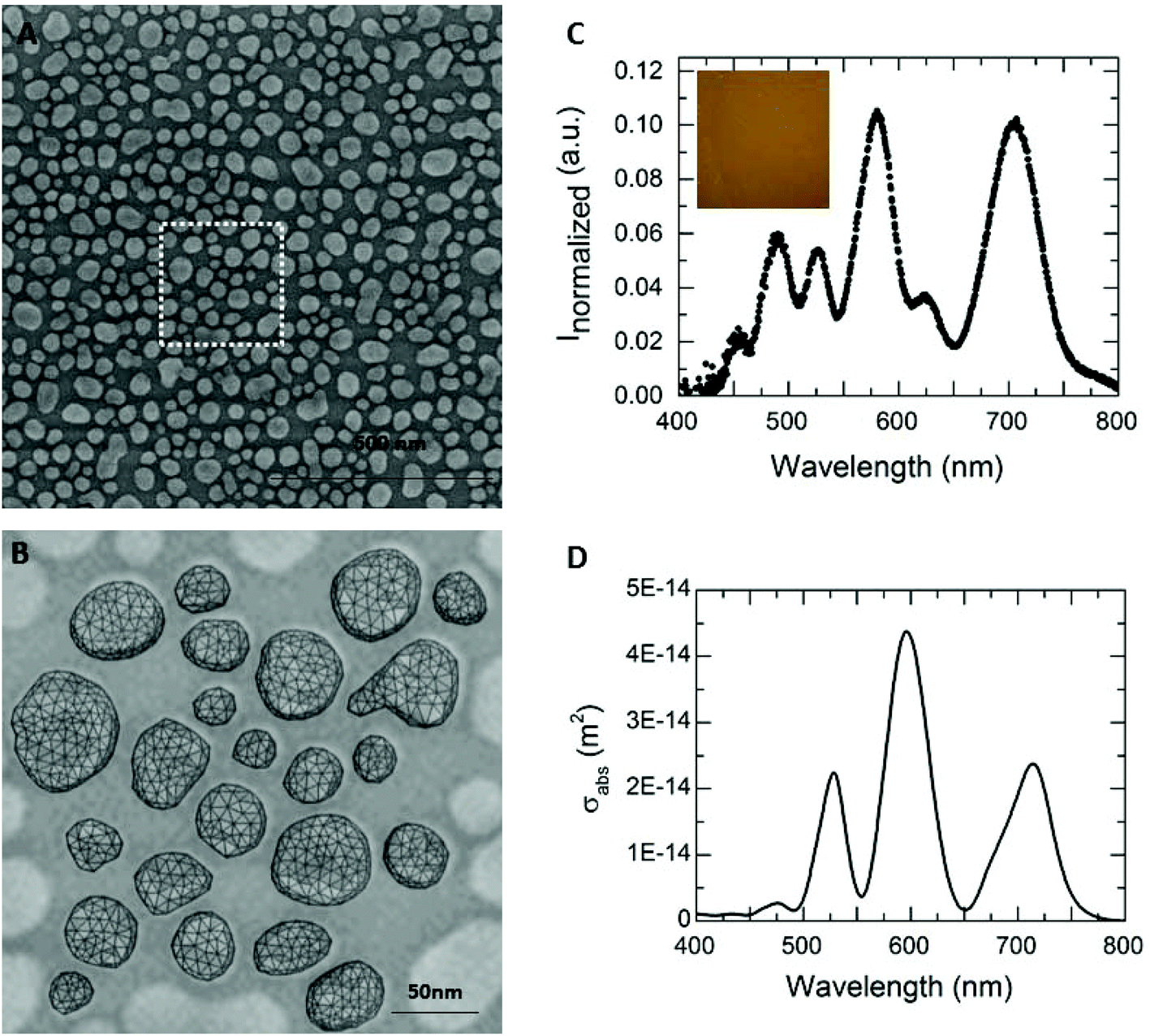 | ||
| Fig. 1 (A) 1.1 by 1.1 μm2 SEM image of a silver SERS active substrate prepared on silicon wafer. (B) Example of a 300 × 300 nm2 3D FEM meshed region extracted from the SEM image. (C) Experimental dark field scattering spectra of the silver particle film deposited on a silicon substrate. The inset of the figure shows the dark field microscopy image. (D) Calculated far-field spectrum from the SERS active substrate simulated with a 2 nm gap distance from the silicon surface (see the main text). | ||
Fig. 1B shows a 300 × 300 nm2 region of Fig. 1A (see the corresponding white rectangle) where the silver particle surface has first been parametrized and then 3D meshed using FEM. This area size has been selected as being large enough to provide a statistically representative distribution of the sample characteristics while preserving nm scale details of the complex individual structures composing it (mesh element size of 9.6 nm for nanometer scale information). The particular goal here is to parametrize a realistic structure for the FEM calculation and to investigate the capability of simulating far- and near-field spectra that are reliable and consistent with real experiments, and this, within an acceptable calculation time. As such, from the view point of a SERS experiment, this area would represent a region slightly below the diffraction limit. SEM was selected for extracting the imaging parameters due to its simplicity and capacity to provide nanoscale structural details of comparatively large areas.38 Conceptually, any scanning probe technique could have been used; however, in this case, tip convolution effects must be considered.39 Due to the absence of depth contrast, SEM solely provides information on the lateral characteristics. Consequently, a particle height of 20 nm was used for all simulations. This value is in agreement with the substrate preparation parameters and with the AFM data.36
An important prerequisite to accurately evaluate the plasmon resonance is having knowledge on the refractive indices of all media involved, as this greatly influences the plasmon resonance.40,41 In a perfect scenario, one considers the refractive index of the silver particle itself, the air surrounding it, and, last but not least, the silicon substrate. The real situation is more complex due to the formation of an amorphous silicon oxide layer (of a typical thickness of a few nanometers42,43) at the particle/silicon wafer interface that cannot be neglected. Adding another layer of amorphous oxide in the FEM simulations would increase the computational efforts considerably. To overcome this challenge, we assumed an air gap of 2 nm between the particle and the pure Si substrate for all surfaces investigated. The detailed description and justification of the procedure are provided in section 2 of the ESI (Fig. S2 and S3†), while section 3 provides more details of the formalism of the FEM calculation (S4, ESI†). It is worth stressing that the refractive index of the underlying substrate and the thickness of the particle are the only parameters that are adapted to fit the dark field experiments while all other parameters depend solely on the size and shape provided by the SEM images. In essence, the method described here is characterized by the lowest possible number of variables, leading to a very low degree of freedom of the system.
Fig. 1C shows the far-field spectrum measured by dark field spectroscopy (measured as the scattering intensity as a function of the wavelength) for the film shown in Fig. 1A measured with a low numerical aperture objective (NA = 0.13, 5×). Under these conditions, the spectral response is highly repeatable (see a spectrum from another section of the same film in Fig. S5† that is similar, but of course not a perfect match) even though the topography itself differs from one region of the sample to the other. This spectrum is used to evaluate the simulation procedure and essentially shows two main bands (580 nm and 710 nm) and a few more minor modes. The inset of the figure shows the dark field microscopy image of the same probed region. Its resulting yellow-orange color could hardly have been predicted solely from the experimental spectroscopy results due to the complexity of the spectral features. Interestingly, the simulation (Fig. 1D showing the modelled absorption cross section) and the experimental data match well, i.e. the major absorption peaks can be found at considerably similar wavelengths. The simulation results exhibit only a slight red shift in comparison with the experimental spectrum. Consequently, this means that the selected area is sufficient to represent the sample. Particularly the particle geometries, sizes as well as the inter-particle distance distribution reflect the optical properties of the entire sample. The differences between the model and the experiment can consequently be attributed to small deviations between the selected parametrized and the experimentally probed areas and/or to the different emphases regarding the finite area of the model that naturally will see a different area-to-circumference ratio compared to the actual laser spot. Based on the calculation procedure, the surface dependence (or more specifically, the surface refractive index dependence) varies for different modes (for details see Fig. S3 of the ESI†). The same procedure was applied for two different regions of the same film (for details see Fig. S6 of the ESI†) and for other similar films, leading to virtually identical results. Hence, we conclude that both the gap distance and the selected area (though much smaller than the experimentally probed region) are adequately selected to describe the optical properties of the system via simulation.
In order to gain a deeper understanding on the nature of the plasmon modes measured by dark field spectroscopy, we reproduced the far-field spectra of Fig. 1D in Fig. 2 to investigate the scattered field (top row of Fig. 2A) and charge density distribution images (2nd row of Fig. 2A) modelled at several wavelengths. Images have been extracted at 10 nm steps over the spectral range presented, but for clarity, only representative examples of close to- and off-resonance conditions are shown. At first glance and considering the large particle size distribution of the SERS substrates, one could expect that single dipole resonances will dominate the spectra and that the three bands are associated with three major particle average sizes. In contrast, an in-depth comparison of the two types of images reveals some remarkable features. In the scattered intensity image at 520 nm, for instance, the smaller particles of the distribution are clearly brighter, indicating that single particle dipoles play a major role. However, when considering the charge density distribution at the same wavelength, the situation differs. Particles of all sizes are polarized differently with respect to the incident field polarization (E0), suggesting a strong contribution of inter-particle coupling modes. The scattering/charge distribution images at 580 and 700 nm lead to similar conclusions. Moreover, even under off-resonant conditions (550 and 640 nm), where the absorption is low, regions of strong inter-particle dipole interactions exist.
 | ||
| Fig. 2 (A) Scattered field (top row) and charge density distribution (second row) images calculated at the wavelength identified on the figure from the corresponding far field spectrum and selected to be close to- and off-resonance (see the main text). (B) Zoom on super-radiant mode (top), sub-radiant mode (middle) and Fano resonance (bottom) extracted from the images in A. The modes have been assigned according to ref. 48 and 49. | ||
The details of the charge density distribution highlight that three major coupling features contribute to the far-field spectra. Examples, extracted from Fig. 2A, are presented in Fig. 2B. The top image presents a dipole bonding (or super-radiant) mode formed when the positive side of the charge density distribution of one particle faces the negative side of the charge density distribution of a neighboring particle, thus locally forming a hybridized system. The middle panel shows a typical example of the reverse situation, i.e. a dipole anti-bonding (sub-radiant mode) where the positive (or negative) charge polarization of two adjacent particles face each other. It must be emphasized that the occurrence of coupling modes over the whole film area, for a system showing such important irregularities and characteristic distribution, is unexpected. Indeed, the strength of the hybridization is known to be correlated with the proximity of the particle,17,44,45 but it also relies on the particle sizes, making the occurrence of the field overlap (as well as its strength) challenging to predict, except for small local regions where the particles are very close to one another.
Most importantly, the lower section of Fig. 2B exposes that even larger scale hybridization such as Fano modes are also present in the system. By definition, a Fano resonance arises from the coupling of a broad bright mode (far-field) with a narrow purely dark mode (near-field),17,46 although there are some exceptions where the coupling of two bright modes can also occur.47 This mode typically implies the hybridization of several (three or more) particles organized in a specific geometrical pattern, thus presenting well-defined organization where the interparticle distance is both well controlled and small. Fig. 2B presents an example of such a structure found in our substrate that consists of four particles. The basic structure resembles a 2D projection of a pyramid prism and is similar to a basic unit of Fano resonances.48,49 The major difference is that our sample has a much lower symmetry and, most importantly, that the structure is composed of particles of different sizes. Interestingly, no clear and isolated features could be found in the far-field experimental (or simulated) spectrum that would have led to the conclusion of the presence of Fano like patterns. Our hypothesis is that structural irregularities contribute by broadening any related bands of the far field spectra. This distribution of characteristics causes the resulting Fano bands to be superimposed by other major modes. For all wavelengths investigated, super-radiant and sub-radiant modes could easily be found and appear to qualitatively constitute a large portion of the images. Fano modes on the other hand are rare, probably due to the larger size of the structures versus the limited simulated sampling area.
The results imply that each spectral band is a superposition of single dipole resonances and complex coupling modes. In our case, and based on the scattering images, we do not expect that the hybridized modes dominate the signal in the far-field spectra at a given wavelength. However, the contribution of the coupling modes to the spectral shape is clearly non-negligible and illustrates the complexity of the system under investigation. Hence, it also emphasizes the need for the presented in-depth theoretical modeling of realistic SERS-active substrates. As mentioned above, so far this information has never been extracted from such samples, but is likely to have profound impact on the interpretation of realistic plasmonic substrate behavior.
To understand the field properties at the surface and the influence of the coupling modes on its enhancement, spectra were also modeled in the near-field at three arbitrarily chosen locations (P1, P2 and P3) indicated on the parametrized surface of Fig. 3A. The associated spectra should be understood as the field enhancement experienced by a molecule situated at those locations. The points have been selected as being close to the edge (P1), and within the particle cluster (P2 and P3). Results from the point P1 (black curve) show a resonance center at ∼520 nm, i.e. at a position that is consistent with one of the bands appearing in the far-field spectra of Fig. 1 and 2. The field enhancement is fairly large (∼40) and the band is narrow, suggesting the dominance of a single dipole resonance. Since P1 is far away from any other particle, the minor modes can hardly be explained by single dipoles of the surrounding particles. Thus, the modes centered at ∼580 and 700 nm, in particular, most likely arise from the involvement of this specific particle in a coupling mode. To investigate the effect of hybridization on the near-field behavior, point P2 was selected purposely several nm away from any particle while still being in a region where the surrounding particles are involved in hybridized modes (see Fig. 2). As such, the location P2 (dark blue curve) is not intended to be a position of high field enhancement, but rather as a position where interparticle coupling is expected to dominate. The low enhancement factor (∼6) and the broader band shape are consistent with this hypothesis. Interestingly, the spectrum is still dominated by a single band at ∼600 nm, which suggests again the dominance of the single dipole resonance from one of the closest particles. For comparison, the light blue curve of the same figure shows the near-field spectrum calculated at a third location, P3, much closer to one of the particles of the cluster. This position is expected to cause the appearance of a dominating single dipole at a higher wavelength position in comparison with P1 due to the bigger size of the closest particle. The global field enhancement increases as compared to P2, but is still only about half of the value reported for P1. Additionally, the clear presence of two bands of close to equal relative intensities clearly exposes the dominant contribution of interparticle hybridization at certain wavelengths. In particular, when comparing P2 and P3 (as well as the particle size close to P1), one can conclude that the mode centered at ∼520 nm, for this particular P3 location, is dominated by the hybridization of the closest particles. From this perspective, the second broad and asymmetric band centered at ∼580 nm must be due to a combination of the single dipole resonance arising from the closest particle and from the hybridized modes in which it is involved. Thus, as expected from the mode analysis of Fig. 1, the near-field response of a virtual molecule is simultaneously position, amplitude and wavelength dependent, which is in accordance with previous studies.50 This brief analysis of the near-field response is far from being statistically relevant, but highlights interesting features. A more systematic investigation of the relative amplitude of the coupling with respect to a single dipole as a function of the spatial location will be subject of future investigation.
 | ||
| Fig. 3 (A) Parametrized SEM surface of a SERS-active substrate indicating the three spatial localization (P1, P2 and P3) for which the near-field has been simulated (B). | ||
Application of the FEM-based method to TERS tips
The FEM-based method described in the previous section can also be transposed for in-depth investigation of the optical properties of virtually any other plasmonic substrate. To illustrate the concept, we have investigated TERS tips prepared by PVD with the use of a standard procedure established by our group.51Fig. 4A shows the SEM image of the resulting probes, namely a pyramid shaped commercially available silicon tip homogeneously covered by silver particles and resembling the structure of the SERS active substrate shown in Fig. 1A. It has been demonstrated that such tips can theoretically be described with the help of a few (if not one) particles situated at the apex when considering subnanometer scale surface defects.31,52,53 The conclusions of these investigations potentially justify the impressively high field enhancement and spatial resolution experimentally observed in TERS.4,54,55 However, on another scale, it is expected that the position and/or amplitude of the plasmon resonance is in fact largely influenced by the close proximity of other surrounding particles.44 As such, larger regions of the system have to be taken into account for accurately evaluating the optimal experimental conditions under which one should work to optimize the signal arising from such a small nanoscale area. Unfortunately, experimental techniques such as dark field spectroscopy are not applicable in the context of TERS tips, because the scattering from the silicon edges is detrimental to the evaluation of the plasmon resonance of the tip only (unless modified set ups with evanescent wave excitation are used56). A reliable theoretical description is consequently extremely useful and necessary. | ||
| Fig. 4 (A) SEM image from a TERS tip with a silver particle film. (B) 300 × 300 nm2 parametrized surface with meshed 3D particles for the FEM calculation. (C) Simulated far-field spectrum from the tip calculated with the incident field polarization (E0) indicated. The red dashed curve is a guideline for what the experimental plasmon resonance is expected to be. The inset shows the charge density distribution calculated for an excitation line of 550 nm. (D) Near-field resonance calculated at locations PT1 and PT2 as indicated in B (full green and blue lines, respectively). The dashed lines refer to the same positions, but where only the single particle closest to the respective locations was parametrized. PT1* and PT2* thus present the near-field response originating solely from the single dipole resonance arising from those two particles (see the main text). | ||
The 300 × 300 nm2 parametrized surface used for the simulation is shown in Fig. 4B and is extracted from the section delimited by the white dashed rectangle in A. To simplify the problem, a region away from the tip apex has been selected (where no curvature from the apex comes into play). In the context of an experiment, this region would still be in the focus region of the laser beam and thus, should be representative of the plasmonic response of the tip. Considering a typical bottom-up configuration and the form factor from the tip itself (a single flat facet of the pyramid), the tilt angle between the incident beam and the tilt of a facet of the tip (with respect to the substrate normal) has been evaluated as ∼10°. This angle corresponds to low NA objectives, similar to that of Fig. 1 and thus, the simulation procedure was applied using the same parameters.
Fig. 4D shows the modeled far-field spectra for two different incident field polarizations (E0x and E0y, grey and black curves, respectively). The spectra show two broad modes with slightly different relative amplitudes, indicating the close to isotropic response of the film as well as the reproducibility of the simulation procedure. Based on experiments, we hypothesize that these two bands can be understood as one single broad feature (see the added red dashed line) centered at ∼560 nm. The fine structure is likely due to the small number of particles considered. In reality, averaging can be expected due to the considerably larger experimentally probed section of the tip. The blue shifted band position when compared to the SERS-active substrate (Fig. 1) is at least partially due to the smaller average size of the particle on the tip (12 nm vs. 22 nm – see Fig. S7 versus S1 of the ESI†).
As was the case for the previously parametrized substrates (Fig. 2), the complexity of the system is more evident when looking at the charge density distribution (see the 550 nm selected example in the inset of Fig. 4C). The general pattern formed is similar to that reported for the previous substrate (Fig. 2), where super-radiant and sub-radiant modes are clearly present. Consequently, Fig. 4D confirms that, not surprisingly, in the optical near field, the situation is complex and highly position dependent. By analogy with a TERS experiment, consider that PT1 (for point TERS 1) refers to a point where a potential molecule would be situated. The point is chosen close to a metallic particle situated at the edge of the picture, such that, in our gedankenexperiment, it could be the last particle of a tip apex. This location is totally random and any point in the outer region of a particle situated at the edge of the image could have been chosen. One must also consider that this imaginary molecule (PT1) would be situated beneath the last particle. The field enhancement experienced by this molecule (at the location PT1) is indicated by the blue curve, where a single intense resonance appears and is associated with an impressively large field enhancement of ∼60. If a second point, PT2, is selected (green curve of Fig. 4D), a single resonance again occurs with a similar enhancement of ∼55, but is red shifted by almost 100 nm compared to PT1. This shift is unexpectedly large when considering that the two particles chosen for this demonstration are of similar size (with an incident polarization in the X direction) and are both situated at the edge of the image, i.e. where less inter-particle coupling is expected. To clarify the relative importance of the single dipole versus the coupling modes, we parametrized the surface such that all particles are eliminated except the ones directly beside PT1 and PT2 (see the modified parametrized surface of Fig. S8† and the corresponding darker particles of Fig. 4B). The near-field spectra computed for both points (PT1* and PT2*) are shown as dashed green and blue curves in Fig. 4D, respectively. In this second set, the particles are hundreds of nanometers away from each other and thus, the absence of interparticle coupling can be assumed. As such, the PT1* and PT2* set of spectra can be understood as the optical response arising solely from dipole resonances. Surprisingly, the computations for the isolated particles (dashed lines) and entire surface (solid lines) match in terms of the band position for both PT locations. In contrast to the first assumption, the influence of other surrounding particles is small in terms of the position of the plasmon resonance for the locations investigated. The shift observed between the PT locations must thus rather be related to the differences of particle morphology or their interaction with the substrate (or potentially a combination of both). The substrate effect is evident when the same TERS-active tip is investigated using a gap distance of 50 nm (thus with the particles virtually in air) and using again only the two parametrized particles. Here, both the field enhancement and spectral shift between the PT points are much less pronounced (for details see ESI Fig. S9†). This suggests that the large wavelength dependence with respect to the contact area of the particles with the substrate (and thus, their morphology) is closely related to the high refractive index of the silicon substrate.
The specific role of the coupling modes becomes obvious when comparing the relative intensities PT vs. PT* pairs of Fig. 4D. When removing all interparticle coupling possibilities, the global field enhancement decreases. For instance, the comparison of PT2 and PT2* highlights that coupling can contribute close to 50% of the total field enhancement while it contributes less than 10% for the PT1 site. The large shift observed between these two particles with such similar sizes is again related to the nature of the substrate, in particular to the refractive index and particle/substrate contact area.
Several conclusions drawn from the model can be transposed to the experiment: (1) as expected, the signal enhancement will change (sometimes dramatically) from tip to tip because the ending particle will never be precisely identical. On the other hand, it also means that, through the modifications of the particle size and shape, the enhancement can be predicted and tuned according to the experimental requirements. (2) Hybridized modes contribute to the field enhancement, but the frequency of the plasmon resonance can be deduced by considering the size and shape of the very last particle at the tip apex. Thus, for a correct description of the optical response of the TERS tips discussed here a certain number of particles is required. This is in accordance with the theoretical investigations made by Taguchi et al.52 and Tserkezis et al.50 although both studies predicted a simultaneous frequency shift that seems to be less pronounced in our study. We believe that the chain modes predicted in the literature that are expected to induce a large shift with particle addition (or chain length increase)50,57 are simply situated outside the visible spectral region under investigation. (4) Given the particularly narrow shape of the near-field bands, the |E|4 approximation used for evaluating the Raman signal enhancement can lead to a large overestimation and must therefore be used carefully. Finally, (5) the enhancement and tunability of the wavelength dependence can also be partially controlled by adjusting the refractive index of the substrate. A closer investigation of the influence of coupling modes on critical parameters such as field confinement and enhancement is beyond the scope of this study. In fact, to the best of our knowledge, the occurrence of hybridized modes has never been reported as being part of the field behavior in the focal area of the tip. This finding on its own thus represents a significant breakthrough in the field and will be a subject of future investigations.
In summary, we have demonstrated that a FEM-based methodology in combination with SEM images (that could be applied on any type of substrate) can be used to simulate in a reliable and accurate manner the far- and near-field optical response of realistic 3D SERS active substrates. Far-field simulation results are shown to match with experimental dark field spectra. A detailed analysis of the scattering and charge distribution images reveals complex plasmon coupling modes, including modes that are primarily observed for highly symmetric SERS-active substrates. These modes have a major impact on the field enhancement, spatial distribution and wavelength dependence. It could be shown that the same conclusions are also valid for TERS tips composed of a thin silver coating. In general, the method is ideally suited for samples that are otherwise challenging to model due to their intrinsic shape and whose localized plasmon resonance can hardly be assessed experimentally. The results reveal that the resonance frequency of the frontmost particle is only weakly influenced by the presence of surrounding particles, but these particles can have a large impact on the field enhancement. The single dipole resonance is also strongly correlated with the particle/substrate contact area and thus, with the particle morphology. A simpler model considering e.g. a sphere will, hence, provide only estimates with respect to plasmon frequency and amplitude. In conclusion, the presented combination of SEM-based parametrization and subsequent FEM-based modelling provides insights into the details of realistic SERS and TERS features. The in-depth study of field enhancement on realistic 3D plasmonic substrates described here represents a promising avenue to solve several of the current analytical issues in the field of SERS and TERS by enabling predictive studies of the amplitude and of the physical origin of field enhancement at different locations. Thus, from a general point of view, this study highlights the necessity for investigating complex optical behaviors that involve numerous inhomogeneous and asymmetrically shaped plasmonic objects.
Experimental section
Sample preparation
All SERS-active substrate films were prepared by a PVD method with subsequent annealing at 290 °C for 60 s, following a protocol described in detail previously.8 The pre-cleaned silicon wafer on which the particles were formed was tilted by ∼15° to mimic the angle of silicon AFM tips (used for the TERS-active tips) to facilitate the comparison between the two types of plasmonic samples. The TERS active tips were produced using a similar procedure, by evaporating a silver particle film on commercial AFM tips (Tap150Al-G, BudgetSensors).Dark field spectroscopy and imaging
Dark field spectra and images were recorded using an upright optical microscope (AxioImager Z1.m from Carl Zeiss) using polychromatic illumination from a halogen light source (100 W) as schematized in Fig. S10 of the ESI.† A central aperture stop blocked the inner part from the illuminated area in order to allow only scattered light from the sample to be detected by the optical camera (MRC5 RGB from Carl Zeiss, Germany) (for direct imaging) or via a multi-mode fiber (∅ = 200 μm), in the microscope image plane, to a spectrometer equipped with a CCD camera (SpectraPro 2300i and Pixis 256 from Princeton Instruments). A grating of 150 lines per mm was used and the central wavelength was fixed to 550 nm. For controlling the spectroscopic area, a pinhole (∅ = 100 μm) was placed in front of the fiber. All spectra were recorded with an exposure time of 10 s and using a 5× EC Epiplan (NA = 0.13) objective.SEM imaging
SEM measurements were performed using a high resolution field emission scanning electron microscope (JSM 6300F, JEOL, Tokyo Japan). The best conditions for imaging in BSE (backscattered electron) contrast provided the primary electron beam at 5 keV. Due to its excellent performance at low electron energy a so called YAG (YttriumAluminum-Garnet) was used as BSE-detector.Computational details
For calculating the electric fields of complex particle films, Finite-Element-Method (FEM) implemented in Comsol Multiphysics 4.4 software was used to solve Maxwell's equation for stationary problems. For all calculations, the constructive relationship for linear materials (σ = 0, μr = 0) was applied. Cubical systems (600 nm × 600 nm) with outer perfect match layers (PML) were used as physical domains. The PML domain consisted of five layers with a PML scaling factor of 1 and was implemented to absorb all scattered light. The incident field oscillated in the x direction with a k-vector in the –z direction. The absorption cross section (σabs) was calculated by integrating the power loss density (Q) over the particle volume (V), were I0 is the incident intensity.
The complex topography of the film was extracted from the SEM images using a parametric surface. The height (approx. 20 nm) of the particle films was based on experimental data and the complex refractive index of the silver particles was adjusted according to Johnson and Christy.58
Conflicts of interest
There are no conflicts to declare.Acknowledgements
V. Deckert acknowledges the support via the German Science Foundation (TRR 166 – A2), the European Union COST Action MP 1302 (Nanospectroscopy) and the Thuringian State Government through its ProExcellence Initiative (ACP2020) (VD and ST). MRL is grateful for the financial support of the NSERC.References
- R. H. Ritchie, Phys. Rev., 1957, 106, 874–881 CrossRef.
- W. R. Holland and D. G. Hall, Phys. Rev. B: Condens. Matter Mater. Phys., 1983, 27, 7765–7768 CrossRef.
- E. Hutter and J. H. Fendler, Adv. Mater., 2004, 16, 1685–1706 CrossRef.
- M. Richard-Lacroix, Y. Zhang, Z. Dong and V. Deckert, Chem. Soc. Rev., 2017, 46, 3922–3944 RSC.
- K. L. Kelly, E. Coronado, L. L. Zhao and G. C. Schatz, J. Phys. Chem. B, 2003, 107, 668–677 CrossRef.
- P. Bazylewski, S. Ezugwu and G. Fanchini, Appl. Sci., 2017, 7, 973 CrossRef.
- N. Rotenberg and L. Kuipers, Nat. Photonics, 2014, 8, 919 CrossRef.
- E. P. Bellido, G. D. Bernasconi, D. Rossouw, J. Butet, O. J. F. Martin and G. A. Botton, ACS Nano, 2017, 11, 11240–11249 CrossRef PubMed.
- M. Richard-Lacroix, Y. Zhang, Z. Dong and V. Deckert, Chem. Soc. Rev., 2017, 46, 3922–3944 RSC.
- S. Kawata, T. Ichimura, A. Taguchi and Y. Kumamoto, Chem. Rev., 2017, 117, 4983–5001 CrossRef PubMed.
- S.-Y. Ding, E.-M. You, Z.-Q. Tian and M. Moskovits, Chem. Soc. Rev., 2017, 46, 4042–4076 RSC.
- M. Quinten and U. Kreibig, Appl. Opt., 1993, 32, 6173–6182 CrossRef PubMed.
- V. M. Shalaev, R. Botet and R. Jullien, Phys. Rev. B: Condens. Matter Mater. Phys., 1991, 44, 12216–12225 CrossRef.
- D. Kurouski, N. Large, N. Chiang, N. Greeneltch, K. T. Carron, T. Seideman, G. C. Schatz and R. P. Van Duyne, Analyst, 2016, 141, 1779–1788 RSC.
- A. Bianconi, AIP Conf. Proc., 2003, 652, 13–18 CrossRef.
- M. I. Stockman, S. V. Faleev and D. J. Bergman, Phys. Rev. Lett., 2001, 87, 167401 CrossRef PubMed.
- P. Nordlander, C. Oubre, E. Prodan, K. Li and M. I. Stockman, Nano Lett., 2004, 4, 899–903 CrossRef.
- S.-C. Yang, H. Kobori, C.-L. He, M.-H. Lin, H.-Y. Chen, C. Li, M. Kanehara, T. Teranishi and S. Gwo, Nano Lett., 2010, 10, 632–637 CrossRef PubMed.
- A. Christ, O. J. F. Martin, Y. Ekinci, N. A. Gippius and S. G. Tikhodeev, Nano Lett., 2008, 8, 2171–2175 CrossRef PubMed.
- Y. Sonnefraud, N. Verellen, H. Sobhani, G. A. Vandenbosch, V. V. Moshchalkov, P. Van Dorpe, P. Nordlander and S. A. Maier, ACS Nano, 2010, 4, 1664–1670 CrossRef PubMed.
- T. Atay, J.-H. Song and A. V. Nurmikko, Nano Lett., 2004, 4, 1627–1631 CrossRef.
- S. M. Morton and L. Jensen, J. Chem. Phys., 2011, 135, 134103 CrossRef PubMed.
- A. M. Kern and O. J. F. Martin, Nano Lett., 2011, 11, 482–487 CrossRef PubMed.
- A. Varas, P. García-González, F. J. García-Vidal and A. Rubio, J. Phys. Chem. Lett., 2015, 6, 1891–1898 CrossRef PubMed.
- M. Barbry, P. Koval, F. Marchesin, R. Esteban, A. Borisov, J. Aizpurua and D. Sánchez-Portal, Nano Lett., 2015, 15, 3410–3419 CrossRef PubMed.
- P. Zhang, J. Feist, A. Rubio, P. García-González and F. J. García-Vidal, Phys. Rev. B: Condens. Matter Mater. Phys., 2014, 90, 161407 CrossRef.
- C. Xing and J. Lasse, J. Opt., 2016, 18, 074009 CrossRef.
- A. Varas, P. García-González, J. Feist, F. J. García-Vidal and A. Rubio, Nanophotonics, 2016, 5, 409 CrossRef.
- M. J. McClain, A. E. Schlather, E. Ringe, N. S. King, L. Liu, A. Manjavacas, M. W. Knight, I. Kumar, K. H. Whitmire, H. O. Everitt, P. Nordlander and N. J. Halas, Nano Lett., 2015, 15, 2751–2755 CrossRef PubMed.
- J. A. Scholl, A. García-Etxarri, A. L. Koh and J. A. Dionne, Nano Lett., 2013, 13, 564–569 CrossRef PubMed.
- S. Trautmann, J. Aizpurua, I. Gotz, A. Undisz, J. Dellith, H. Schneidewind, M. Rettenmayr and V. Deckert, Nanoscale, 2017, 9, 391–401 RSC.
- E. M. Perassi, J. C. Hernandez-Garrido, M. S. Moreno, E. R. Encina, E. A. Coronado and P. A. Midgley, Nano Lett., 2010, 10, 2097–2104 CrossRef PubMed.
- J. Burgin, I. Florea, J. Majimel, A. Dobri, O. Ersen and M. Treguer-Delapierre, Nanoscale, 2012, 4, 1299–1303 RSC.
- S. M. Collins, E. Ringe, M. Duchamp, Z. Saghi, R. E. Dunin-Borkowski and P. A. Midgley, ACS Photonics, 2015, 2, 1628–1635 CrossRef.
- E. M. Perassi, C. Hrelescu, A. Wisnet, M. Döblinger, C. Scheu, F. Jäckel, E. A. Coronado and J. Feldmann, ACS Nano, 2014, 8, 4395–4402 CrossRef PubMed.
- R. M. Stöckle, V. Deckert, C. Fokas and R. Zenobi, Appl. Spectrosc., 2000, 54, 1577–1583 CrossRef.
- M. Fan, G. F. S. Andrade and A. G. Brolo, Anal. Chim. Acta, 2011, 693, 7–25 CrossRef PubMed.
- R. Reichelt, in Science of microscopy, Springer, 2007, pp. 133–272 Search PubMed.
- J. Canet-Ferrer, E. Coronado, A. Forment-Aliaga and E. Pinilla-Cienfuegos, Nanotechnology, 2014, 25, 395703 CrossRef PubMed.
- S. Underwood and P. Mulvaney, Langmuir, 1994, 10, 3427–3430 CrossRef.
- M. Schmid, R. Klenk, M. C. Lux-Steiner, M. Topič and J. Krč, Nanotechnology, 2011, 22, 025204 CrossRef PubMed.
- M. Morita, T. Ohmi, E. Hasegawa, M. Kawakami and K. Suma, Appl. Phys. Lett., 1989, 55, 562–564 CrossRef.
- M. J. Kim and R. W. Carpenter, J. Mater. Res., 2011, 5, 347–351 CrossRef.
- R. Esteban, A. G. Borisov, P. Nordlander and J. Aizpurua, Nat. Commun., 2012, 3, 825 CrossRef PubMed.
- D. C. Marinica, H. Lourenco-Martins, J. Aizpurua and A. G. Borisov, Nano Lett., 2013, 13, 5972–5978 CrossRef PubMed.
- B. Luk'yanchuk, N. I. Zheludev, S. A. Maier, N. J. Halas, P. Nordlander, H. Giessen and C. T. Chong, Nat. Mater., 2010, 9, 707–715 CrossRef PubMed.
- A. Lovera, B. Gallinet, P. Nordlander and O. J. F. Martin, ACS Nano, 2013, 7, 4527–4536 CrossRef PubMed.
- D. Dregely, M. Hentschel and H. Giessen, ACS Nano, 2011, 5, 8202–8211 CrossRef PubMed.
- Y. Zhan, D. Y. Lei, X. Li and S. A. Maier, Nanoscale, 2014, 6, 4705–4715 RSC.
- C. Tserkezis, R. W. Taylor, J. Beitner, R. Esteban, J. J. Baumberg and J. Aizpurua, Part. Part. Syst. Charact., 2014, 31, 152–160 CrossRef.
- R. M. Stöckle, Y. D. Suh, V. Deckert and R. Zenobi, Chem. Phys. Lett., 2000, 318, 131–136 CrossRef.
- A. Taguchi, J. Yu, P. Verma and S. Kawata, Nanoscale, 2015, 7, 17424–17433 RSC.
- K. Uetsuki, P. Verma, P. Nordlander and S. Kawata, Nanoscale, 2012, 4, 5931–5935 RSC.
- T. Deckert-Gaudig, E. Kämmer and V. Deckert, J. Biophotonics, 2012, 5, 215–219 CrossRef PubMed.
- T. Deckert-Gaudig, D. Kurouski, M. A. B. Hedegaard, P. Singh, I. K. Lednev and V. Deckert, Sci. Rep., 2016, 6, 33575 CrossRef PubMed.
- C. C. Neacsu, G. A. Steudle and M. B. Raschke, Appl. Phys. B, 2005, 80, 295–300 CrossRef.
- L. O. Herrmann, V. K. Valev, J. Aizpurua and J. J. Baumberg, Opt. Express, 2013, 21, 32377–32385 CrossRef PubMed.
- P. B. Johnson and R.-W. Christy, Phys. Rev. B: Solid State, 1972, 6, 4370 CrossRef.
Footnote |
| † Electronic supplementary information (ESI) available. See DOI: 10.1039/c8nr02783h |
| This journal is © The Royal Society of Chemistry 2018 |