
 Open Access Article
 This Open Access Article is licensed under a Creative Commons Attribution-Non Commercial 3.0 Unported Licence
Quantified hole concentration in AlGaN nanowires for high-performance ultraviolet emitters†
Chao
Zhao
 a,
Mohamed
Ebaid
a,
Huafan
Zhang
a,
Davide
Priante
a,
Bilal
Janjua
a,
Daliang
Zhang
b,
Nini
Wei
b,
Abdullah A.
Alhamoud
a,
Mohammad Khaled
Shakfa
a,
Tien Khee
Ng
*a and
Boon S.
Ooi
*a
a,
Mohamed
Ebaid
a,
Huafan
Zhang
a,
Davide
Priante
a,
Bilal
Janjua
a,
Daliang
Zhang
b,
Nini
Wei
b,
Abdullah A.
Alhamoud
a,
Mohammad Khaled
Shakfa
a,
Tien Khee
Ng
*a and
Boon S.
Ooi
*a
aKing Abdullah University of Science and Technology (KAUST), Photonics Laboratory, Thuwal 23955-6900, Saudi Arabia. E-mail: tienkhee.ng@kaust.edu.sa; boon.ooi@kaust.edu.sa
bKing Abdullah University of Science and Technology (KAUST), Imaging and Characterization Core Lab, Thuwal 23955-6900, Saudi Arabia
First published on 29th May 2018
Abstract
p-Type doping in wide bandgap and new classes of ultra-wide bandgap materials has long been a scientific and engineering problem. The challenges arise from the large activation energy of dopants and high densities of dislocations in materials. We report here, a significantly enhanced p-type conduction using high-quality AlGaN nanowires. For the first time, the hole concentration in Mg-doped AlGaN nanowires is quantified. The incorporation of Mg into AlGaN was verified by correlation with photoluminescence and Raman measurements. The open-circuit potential measurements further confirmed the p-type conductivity, while Mott–Schottky experiments measured a hole concentration of 1.3 × 1019 cm−3. These results from photoelectrochemical measurements allow us to design prototype ultraviolet (UV) light-emitting diodes (LEDs) incorporating the AlGaN quantum-disks-in-nanowire and an optimized p-type AlGaN contact layer for UV-transparency. The ∼335 nm LEDs exhibited a low turn-on voltage of 5 V with a series resistance of 32 Ω, due to the efficient p-type doping of the AlGaN nanowires. The bias-dependent Raman measurements further revealed the negligible self-heating of devices. This study provides an attractive solution to evaluate the electrical properties of AlGaN, which is applicable to other wide bandgap nanostructures. Our results are expected to open doors to new applications for wide and ultra-wide bandgap materials.
Introduction
Ultraviolet (UV)-light sources, especially group III nitride-based UV-light emitters, have attracted interest due to their applications in dermatology, water purification, and solid-state lighting, which can replace non-environmentally friendly gas lasers and mercury lamps.1,2 Because of the lack of low-cost, native substrates, AlGaN-based UV light-emitting diodes (LEDs) are typically grown on sapphire substrates. The lattice and thermal mismatches induce a high dislocation density in AlGaN materials.3 Additionally, the formation of ohmic contacts in p-type materials is problematic, and the current injection efficiency of UV LEDs is limited due to the high ionization energy of the Mg acceptors, low hole concentration of AlGaN, and difficulty in obtaining metals with low Schottky barriers;4–6 the light extraction efficiency is also limited by the absorption of the p-GaN contact layer used in the structure.7 The GaN![[thin space (1/6-em)]](https://www.rsc.org/images/entities/char_2009.gif) :Mg p-type contact layer when replaced with UV-transparent AlGaN:Mg resulted in an increase in the operating voltage due to the low hole concentration.8 Furthermore, the low conductivity of the AlGaN layer in UV LEDs leads to severe junction heating.9,10 Since the lifetime and efficiency of LEDs decrease as the junction temperature increases, their resistive heating must be reduced while heat dissipation must be improved.11 Apparently, the p-type doping is one of the major issues limiting the performance of UV LEDs.12–14
:Mg p-type contact layer when replaced with UV-transparent AlGaN:Mg resulted in an increase in the operating voltage due to the low hole concentration.8 Furthermore, the low conductivity of the AlGaN layer in UV LEDs leads to severe junction heating.9,10 Since the lifetime and efficiency of LEDs decrease as the junction temperature increases, their resistive heating must be reduced while heat dissipation must be improved.11 Apparently, the p-type doping is one of the major issues limiting the performance of UV LEDs.12–14
Recently, group III-nitride nanowire devices have shown advantages over conventional planar devices, such as dislocation-free material growth on low-cost substrates,15–18 a relaxed strain and reduced polarization field,19 and enhanced extraction of the transverse magnetic (TM)-polarized photons for UV LEDs.7,20 Moreover, the Mg-dopant incorporation into nanowires is more efficient because of the lower formation energy.21–23 The internal electric field from N-polar nitride nanowires grown by molecular beam epitaxy (MBE) can also enhance the hole injection.24–26 In this regard, Al(Ga)N-based UV LEDs,27–29 UV random lasers,21,29–31 photodetectors,32 and single photon sources33 have been demonstrated. To take advantage of the benefits of nanowires in devices, the doping level and electrical properties of the AlGaN nanowire array must be characterized. Various methods have been developed for single nanowires, such as the Hall effect,34 field effect transistor,35 and photoconductivity measurements.36 However, these measurements involve challenging processing procedures. Moreover, the composition and doping fluctuations in/between AlGaN nanowires strongly influence the electrical properties of the nanowire array.31,37,38 The hole concentration in nanowire arrays is typically estimated using a planar GaN:Mg epilayer as a reference.30 However, a discrepancy exists between the estimated and actual values because of different morphologies and growth conditions. Photoelectrochemical (PEC) measurements of GaN nanowires directly provide an average value of charge carrier concentration for the entire nanowire ensemble.39 However, to the best of our knowledge, the carrier concentrations of AlGaN nanowires, especially the hole concentration, which are essential for UV emitters, have not been examined and reported. Additionally, nanowires grown on a bulk-metal substrate platform have been proven to dissipate the heat effectively, which is highly desirable to devices based on potentially resistive AlGaN materials.40
Here, we systematically investigated the p-type doping and hole concentration of AlGaN nanowires monolithically grown on molybdenum (Mo) substrates for the first time. The incorporation of Mg was confirmed by the donor-bound exciton (D0X) and donor–acceptor pair (DAP) peaks in the photoluminescence (PL) spectra and the Mg-related local vibrational modes (LVMs) presented in the Raman spectra. By the meticulous preparation of PEC cells for reliable Mott–Schottky measurements, an accurate hole concentration can be obtained. The open circuit potential (OCP) measurements confirmed the transition from an n-type to p-type conductivity in AlGaN as the Mg doping increased; Mott–Schottky measurements showed a maximum hole concentration of 1.3 × 1019 cm−3 for the AlGaN nanowires.
Moreover, by cross calibrating MBE growth conditions with hole concentration from Mott–Schottky measurements, we managed to replace the GaN:Mg p-type contact layer of UV-emitting AlGaN nanowire-LEDs using UV-transparent AlGaN:Mg with optimized p-type doping, while maintaining a low turn-on voltage. The AlGaN/AlGaN quantum-disks (Qdisks)-in-nanowire, core–shell UV LEDs were epitaxially grown on Mo substrates, which provides a three-dimensional carrier confinement.41 The LEDs emit at ∼335 nm and exhibit a low turn-on voltage of 5 V and a series resistance of 32 Ω, which are attributed to the high crystal quality and low hole activation energy, i.e., the efficient p-type doping of the AlGaN nanowires. The bias-dependent Raman measurements (up to 10 V) further revealed the low self-heating of the designed device structure on our metal heat-sink platform. The results presented herein provide an important strategy for accurately evaluating the electrical properties of wide-bandgap nanowire materials and designing nanoscale devices. The combined metal platform and PEC technique are expected to open doors to practical application of ultra-wide bandgap nitrides and oxides which are rapidly developing.2
Experimental
Growth of nanowires and UV LEDs
The p-type AlGaN nanowires and UV LEDs on Mo substrates were grown using a Veeco Gen 930 plasma-assisted MBE system similar to that in our previous reports.40 Before loading into MBE chambers, the 1 cm × 1 cm × 0.05 cm Mo substrates were coated with a 500 nm layer of Ti using an electron beam evaporator. The p-type AlGaN nanowires were grown at 560 °C with TMg between 280 and 440 °C, which is a relatively low growth temperature to enhance the Mg incorporation.42 An intrinsic AlGaN nanowire sample was also grown at the same temperature for comparison. For the UV LEDs, an 80 nm thick layer of n-type GaN was grown and followed by n-type Al0.15Ga0.85N (∼5 nm) and n-type Al0.3Ga0.7N (∼50 nm) for confinement, 15 Al0.14Ga0.86N-disks (∼1.6 nm) separated by Al0.3Ga0.7N-barriers (∼6 nm), and p-type Al0.3Ga0.7N (∼50 nm) grown at an elevated temperature.25 The device structure was completed by a p-Al0.15Ga0.85N layer (∼20 nm) grown at 560 °C for p-contact to avoid absorption loss. Different fluxes were used to achieve the composition required.Nanowire characterization
After the growth, the surface morphologies and crystal quality of the nanowires were characterized using an FEI Magellan FEG field-emission scanning electron microscope (SEM) and a Bruker D8 X-ray diffraction (XRD) instrument with a Cu Kα source. The PL was measured at room temperature (RT) and 77 K using a 266 nm pulsed laser (SNU-20F-100) for excitation to obtain the emission wavelength of the AlGaN nanowires and Qdisks. Raman measurements were carried out on a Horiba Jobin Yvon micro-Raman system using a 473 nm laser for excitation in the backscattering geometry. The PEC characterization of the Mg-doped AlGaN nanowires was performed in a three-electrode cell using the AlGaN nanowires as the working electrode and Pt mesh as the counter electrode with a Ag/AgCl reference electrode (Eref = +200 mV versus the normal hydrogen electrode) in a 1 M H2SO4 electrolyte solution. A solar simulator equipped with a Xe-lamp and an AM 1.5 G filter was used to simulate sun-light illumination during the OCP measurements. Mott–Schottky measurements were performed under dark conditions using a potentiostat with 10 mV amplitude and a wide frequency range from 1 mHz to 10 kHz. For the sake of accuracy, the PEC experiments were repeated with five different samples, and the average value was obtained with reasonable statistical errors considering the geometry fluctuation of the nanowire arrays. To evaluate the structure of the nanowire UV LEDs, we prepared a cross-sectional transmission electron microscopy (TEM) sample using an FEI Helios NanoLab 400 s-FIB/SEM. The structural and chemical integrities of the nanowires were investigated by high-angle annular dark-field scanning transmission electron microscopy (HAADF-STEM) and electron energy-loss spectroscopy (EELS) using a probe-corrected FEI Titan operating at 200 kV. The carrier confinement in the nanowire UV LED structure was modeled using NEXTNANO3, which is a commercially available software.43Device fabrication and test
Nanowire UV LEDs were fabricated and tested. In contrast to our reported InGaN/GaN nanowire LEDs,44 we directly placed 5 nm Ni/5 nm Au on the nanowire top surface to form a p-contact using a tilted-angle deposition technique.45 The light power–current–voltage (L–I–V) characteristics and EL spectra of the UV LEDs were measured under DC injection using a system integrated with a Keithley 2400 source meter, a Newport power meter (Model 2936-C), and an Ocean Optics QE Pro spectrometer. The light output power from the top of the UV LEDs was measured through a UV objective using a Si photodiode connected to the Newport power meter. The current-dependent micro-Raman measurements were carried out using a 785 nm laser in a backscattering geometry to evaluate the junction heating during operation using the AlGaN E2 high-frequency mode Raman peak shift, E2(high).Results and discussion
The SEM images of the Al0.15Ga0.85N nanowires grown at different Mg effusion cell temperatures (TMg) are shown in Fig. 1(a–c). The incorporation of Mg clearly leads to the lateral growth of the nanowires and coalescence between adjacent AlGaN nanowires.46,47 For the highly doped nanowires with TMg of 400 and 440 °C, the morphology completely deteriorated, and a quasi-AlGaN layer formed (Fig. S1, ESI†). Fig. 1(d) shows the 10 K PL spectra of the intrinsic AlGaN nanowires and the doped nanowires with different TMg values. The PL spectrum of the intrinsic AlGaN nanowires is dominated by the D0X peak at 333 nm. In the spectrum of the doped AlGaN nanowires with TMg values from 280 to 360 °C, another low-energy peak appears at 382 nm, which is attributed to the DAP transition between the shallow Mg acceptor states and the VN-related deep donor states.39 For the highly doped AlGaN nanowires with TMg values of 400 and 440 °C, the D0X peak disappears, the DAP peak slightly redshifts, and a broad peak emerges at approximately 500 nm, which is related to the yellow defect luminescence. Moreover, the RT PL was completely quenched in the highly doped AlGaN nanowires (Fig. S2(a), ESI†) due to the degraded crystal quality from the coalescence (see Fig. 1(c)) and the formation of twins and stacking faults.47–49 | ||
| Fig. 1 Plan-view SEM images of the AlGaN nanowires; (a) intrinsic, (b) TMg = 320 °C, (c) TMg = 400 °C. (d) 10 K PL spectra of AlGaN nanowires grown with different TMg values. (e) and (f) Raman spectra of the AlGaN nanowires with different TMg values. The peak at 2330 cm−1 originates from Raman scattering by the N2 molecules in air. | ||
Fig. 1(e) and (f) show the Raman spectra of the Al0.15Ga0.85N nanowires. The E2 high-frequency mode, E2(high), at 567 cm−1 was observed for all the samples. With the Mg doping, the E2(high) mode intensities decreased and the full-width-at-half-maximum (FWHM) increased due to the degraded material quality of the coalesced AlGaN nanowires.50 The longitudinal optical (LO) phonon mode A1(LO) at 752 cm−1 was dominant when the TMg value was higher than 360 °C because the light is backscattered from the quasi-AlGaN layer c-plane surface.39 Moreover, the LVMs at 266 and 657 cm−1, which are due to the incorporated Mg replacing the host-lattice (Ga) atom, and at 2168 and 2184 cm−1, which are due to the Mg–H complexes or nitrogen vacancies for the MBE grown samples, are clearly observed for the nanowires doped with Mg at 360 and 400 °C (Fig. S2(b), ESI†).39,51–55 When TMg was 440 °C, the Mg-related signatures were absent, which was probably due to the different growth modes, i.e., different scattering geometries under this condition. Although we were not able to estimate the Mg concentration for the sample with TMg = 360 °C and 400 °C using intensities of LVMs due to the lack of references for the Mg-doped AlGaN study,39 the Raman results here further affirm the substitutional Mg atoms.
To quantitatively analyze the influence of the Mg doping on the charge carrier concentration, we performed OCP and Mott–Schottky PEC measurements. Firstly, the kinetics of the free charge carriers were investigated by measuring the OCP under dark and illumination conditions. The shift in the OCP with light can indicate the conductivity type of the doped semiconductor materials. Under dark conditions, an n-type semiconductor will exhibit an upward band bending due to the transportation of the excess charge carriers from the semiconductor to the electrolyte to achieve electrochemical equilibrium. Upon illumination, the photogenerated minority charge carriers will shift the quasi-Fermi level of the electrons upward, resulting in a negative shift of the OCP. As shown in Fig. 2(a), while the intrinsic AlGaN nanowires exhibited a negative shift of the OCP, the sample doped with TMg of 360 °C showed a positive shift, which indicated that the conductivity changed from n- to p-type (Fig. S3, ESI†). Another method to determine the change in the conductivity type is to measure the difference in the OCP under dark and illuminated conditions. Negative values indicate n-type conductivity and positive values indicate p-type conductivity. As shown in Fig. 2(b), up to a TMg of 320 °C, the AlGaN nanowires exhibited a negative difference in the OCP, while this difference became positive when the TMg increased to 360 °C. The reduction in the OCP difference at TMg values higher than 360 °C can be attributed to the crystal defects associated with increasing Mg flux, which can act as carrier trapping states to reduce the density of the photogenerated minority carriers and decrease the difference in the OCP.32 These AlGaN nanowires suffered from a severe coalescence and showed a defect-related yellow luminescence peak, as shown in Fig. 1(c) and (d).
 | ||
| Fig. 2 Characterization of the Mg-doped AlGaN nanowires by electrochemical techniques. (a) OCP of the intrinsic sample and a representative Mg-doped sample with a TMg of 360 °C. (b) Calculated OCP values for all samples as a function of TMg. (c) Mott–Schottky plots of the intrinsic and Mg-doped AlGaN nanowires. (d) Summarized net ionized dopant density as a function of TMg. | ||
While the OCP measurements are direct methods to determine the conductivity type of doped semiconductor materials, Mott–Schottky plots can provide a quantitative analysis of the charge carrier concentration, and these plots describe the relationship between the inverse square of the double layer capacitance and the applied potential, which is represented by the following equation:56
 | (1) |
 | (2) |
 | (3) |
The optimized p-type AlGaN was incorporated into a UV LED structure as a transparent contact layer. Fig. 3(a) and (b) show the plan-view and elevation-view SEM images of the nanowire UV LEDs on Mo substrates, respectively. The vertical nanowires have a hexagonal shape with some degree of coalescence, an average length of ∼400 nm, a lateral size of 100–170 nm, a density of ∼1.1 × 1010 cm−2, and tapered from the bottoms. Fig. 3(c) shows XRD results for the initial Mo substrate, the Mo substrate with a 500 nm Ti coating, the GaN nanowires on Ti/Mo, and the nanowire UV LEDs on Ti/Mo. The polycrystalline Mo substrate related peak was not observable in the measurement range. Consistent with previous reports, the Ti coating has a preferential (0002) orientation. Because of the surface nitridation of the Ti layer before the nanowire growth, the Ti(0002) peak remained, and broad TiN(111), and GaN(0002) peaks were obtained after the GaN growth. Thus, the nanowires were grown on the TiN(111) transition layer. The AlGaN(0002) reflection for the UV LEDs was also observed. To evaluate the orientation of the nanowires on the Mo substrate, the X-ray pole figure of the (0002) AlGaN reflection was studied. As shown in Fig. 3(d), the diffracted X-ray beam intensity distributions are located in the center of the pole figure, which indicates that the c-axis of most of the AlGaN nanowires is perpendicular to the substrate and agrees with the θ–2θ scan result.64,65 Moreover, a distribution of the tilt angles of the AlGaN nanowires with the [0002] axis is also expected because of the rough substrate surface. Fig. 3(e) shows the RT PL spectrum of the AlGaN/AlGaN Qdisks in the nanowires. Fig. 3(f) shows the schematic of the nanowire UV LEDs. The Al composition of the Qdisks was tuned to achieve a peak emission wavelength of 335 nm. The emission of Qdisks has a FWHM of 17.3 nm, which is much smaller than UV devices with double heterostructures, and this is attributed to the compositional homogeneity in the nanowires, and uniform Qdisks with a strong carrier confinement, as shown in the TEM results discussed below.28,42
 | ||
| Fig. 3 (a) The plan-view and (b) elevation-view SEM images of the Qdisks-in-nanowires. (c) XRD profiles of the nanowire samples. (d) X-ray pole figure of the AlGaN (0002) reflection. (e) RT PL spectrum of the AlGaN/AlGaN Qdisks-in-nanowires. (f) The schematic of a nanowire UV LED on Mo, the thin n-Al0.15Ga0.85N layer is not shown. | ||
We further examined the crystal quality and structure of the nanowire UV LED on Ti/Mo using cross-sectional TEM (Fig. S6(a) and (b), ESI†). Fig. 4(a) shows a SEM image of the vertical nanowires, the crown-like p-AlGaN layers, Ti layers, and Mo grains from the polycrystalline Mo substrates. It is observed that some nanowires grow away from the [0002] direction because of the rough substrates, resulting in the intensity distribution away from the center in the pole figure (see Fig. 3(d)). Fig. 4(b) shows the high-resolution TEM (HRTEM) image of nanowires. The inset of Fig. 4(a) shows the selective area electron diffraction (SAED) pattern of the nanowires, which confirmed their single-crystal nature and [0002] orientation. The image of the nanowires was obtained along the [2−1−10] zone axis, which is parallel to the facets of the nanowires.66 The high crystal-quality of AlGaN nanowires also helped the Mg incorporation as discussed above. Fig. 4(c) shows the typical HAADF-STEM image of a nanowire, recorded along the same zone axis. The 1.6 nm Al0.14Ga0.86N Qdisks/6 nm Al0.3Ga0.7N barrier, which is the active region of a UV LED, AlGaN shell, and top p-AlGaN layer can be seen. The HAADF images provided the Z-contrast, and the Al0.14Ga0.86N Qdisks (bright color) were separated by Al0.3Ga0.7N barriers (dark color) (Fig. S6(c) and (d), ESI†), which were not affected by the defects at the roots of the nanowires.50Fig. 4(d) shows the interface of GaN/transition layer/Ti layers, and the 15 nm transition layer between the GaN defect-free region and Ti was confirmed to be face-centered cubic TiN with a [111] preferred orientation according to the XRD results and previous study, where the nanowires nucleate and epitaxially grow on.50
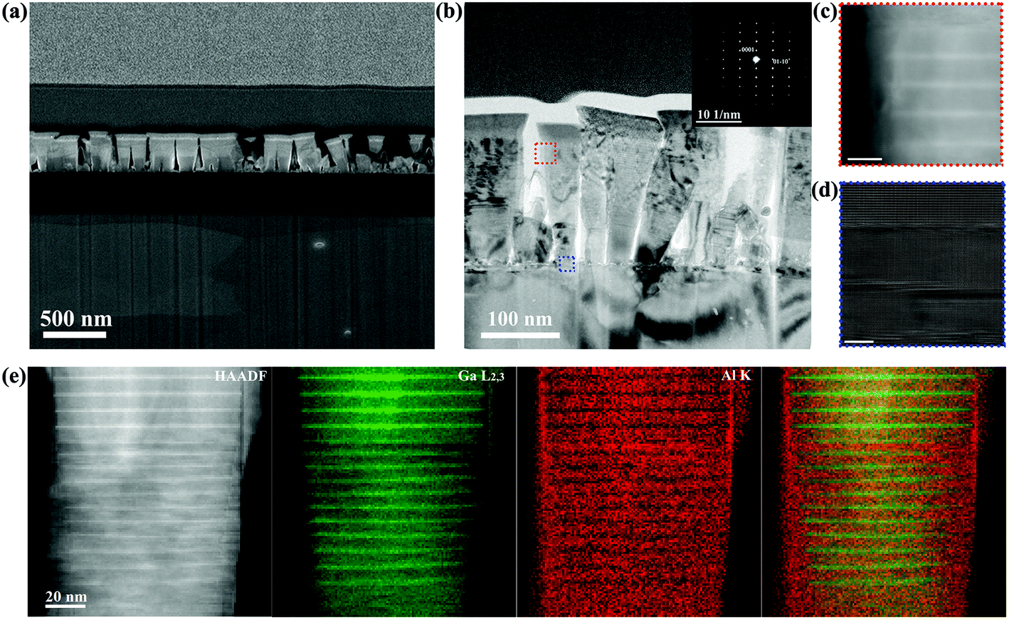 | ||
| Fig. 4 (a) SEM image of a FIB-prepared TEM lamella for the nanowire UV LEDs on Ti/Mo. (b) High-magnification TEM image of the nanowire UV LEDs on Ti/Mo substrates and the corresponding SAED pattern (inset). (c) STEM images of the tops of the nanowires, the scale bar is 10 nm. (d) HRTEM image of the interface between the nanowires and Ti, the scale bar is 5 nm. (e) The false-color Ga and Al elemental concentration maps of the nanowires and a combined elemental map with Ga in green and Al in red. | ||
Elemental analysis was performed on the nanowires using EELS-STEM. The EELS-SI map in Fig. 4(e) shows the Ga and Al elemental distributions in the nanowires. The Ga map extracted from the Ga L2,3-edge shows a lower Al composition in the AlGaN of Qdisks, while the Al map extracted from the Al K-edge shows a higher Al composition in the AlGaN barrier and Al-rich shell, which further confirmed that the AlGaN Qdisks are surrounded by the shell layer and is consistent with other reports.31 The formation of a lateral AlGaN shell with a progressively increasing thickness is attributed to the short diffusion length of the Al adatoms under the growth conditions,67,68 and thus, AlGaN can nucleate at the top and on the facets of the nanowires, which can in situ passivate the surface states on the sidewalls of the nanowires and provide carrier confinement.69,70 The formation of an asymmetric shell, as shown in Fig. 4(c), is likely due to the short diffusion lengths of the Ga and Al adatoms and a shadow effect when the nanowire density is too high.71 The reduced strain and thin Al0.14Ga.86N Qdisks lead to a large electron–hole wavefunction overlap. The calculated recombination rates in the active region show that direct radiative recombination is the dominant form of recombination. Furthermore, the decrease in the barrier height at the n-Al0.3Ga0.7N/GaN interfaces by incorporating an intermediate composition, thin Al0.15Ga0.85N layer (5 nm), can significantly enhance the carrier injection efficiency and quantum efficiency of the UV LEDs (Fig. S7, ESI†).
Nanowire UV LEDs incorporating optimized p-AlGaN top contact and AlGaN/AlGaN Qdisks were fabricated and characterized. Fig. 5(a) shows the current–voltage (I–V) characteristics of the UV LEDs on both linear and logarithm scales. The LED has a low turn-on voltage of ∼5 V and a series resistance of 32 Ω, as indicated by the slope of the I–V curve after the LED turn-on. This is attributed to the high hole concentration of the AlGaN layers and the formation of a TiN contact layer as shown in Fig. 4(d).28,42,72–75 The device also shows good diode characteristics with a negligible leakage current, as depicted in the inset of Fig. 5(a). Fig. 5(b) shows the light output power–current characteristics and the relative external quantum efficiency (EQE) of the LED measured under direct current (DC) injection. The inset shows the image of the illuminated UV LED. In the continuous-wave mode, the light output power was 12.9 μW when operating at 170 mA injection current and ∼10 V forward bias voltage. The LED does not show an efficiency droop due to the increased hole concentration and better heat dissipation in our platform.76 The RT electroluminescence (EL) spectra of the LEDs as the injection currents increased are shown in Fig. 5(c). We achieved a peak emission wavelength at ∼335 nm with a negligible blueshift in the current injection range of 20–150 mA due to the reduced strain-induced polarization field as shown in Fig. S7(c).† No additional peak from the other layers was observed, which indicated reduced carrier leakage in the presence of efficient p-type doping while maintaining crystal quality. We further measured the junction heating of the UV LEDs based on the relative downshift of the AlGaN E2(high) phonon Raman peak of the LEDs under the current injection with respect to the peak position at zero current (Fig. S8, ESI†). As shown in Fig. 5(d), the LED showed insignificant junction heating across the full injection range, and the peak shift was within the resolution of the Raman system. This can be attributed to the absence of a barrier for the carriers and the low resistivity of the p-type AlGaN layers. We believe that the performance of these devices can be further improved by optimizing the growth parameters and the active layer design.
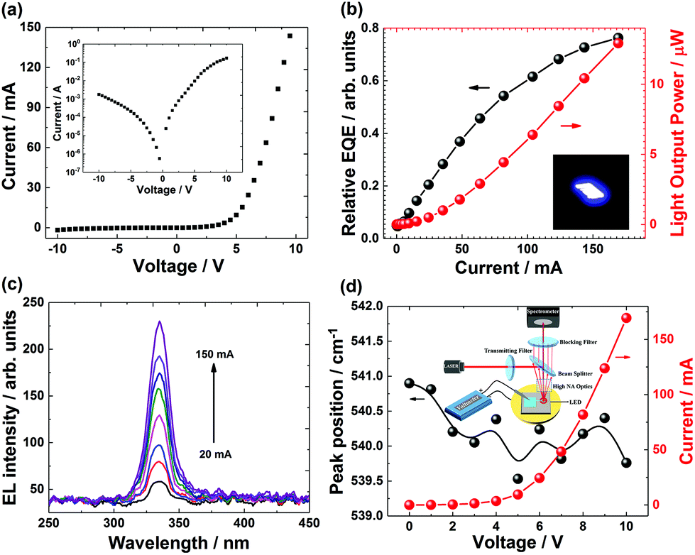 | ||
| Fig. 5 (a) The measured I–V characteristics of the 500 × 500 μm LED; the inset shows the semi-log scale of the I–V characteristics. (b) The light output power and relative EQE of the UV LEDs versus the injected current, the inset shows the optical microscopy image of the illuminated LED. (c) The EL spectra of the LED for injection currents from 20–150 mA. (d) E2(high) peak position and current observed at different bias levels for the UV LED. The inset shows the setup for bias-dependent Raman measurements. | ||
Conclusions
In conclusion, we have achieved a significantly improved Mg incorporation and hole concentration using the low growth temperature, optimized Mg doping conditions, and high crystal quality nanowires. For the first time, we quantify the hole concentration of AlGaN nanowires using PEC methods and measure a hole concentration of up to 1.3 × 1019 cm−3. Furthermore, AlGaN-based UV LEDs with low turn-on voltage emitting at ∼335 nm are designed with the knowledge of the hole concentration. The LEDs on the Mo platform also help to obtain low self-heating of the device. It is noteworthy that the quantified doping of AlGaN nanowires across the entire composition range could be achieved by tuning the growth parameters, and the strategy can be extended to other material systems. The success of applying PEC methods to design devices paves the way towards practical applications of nanowires. Improved performance and new applications for nanoscale devices based on wide-bandgap materials can be envisioned.Author contributions
C. Z. conceived the idea and designed the experiments and the fabrication process. M. E. and H. Z. performed the PEC experiments. C. Z., D. P., and A. A. A. performed the Raman measurements and tested the devices. C. Z., D. Z, and N. W. performed the TEM and FIB analyses. M. K. S. performed the PL measurements. B. J. performed the Nextnano simulation. C. Z., T. K. N., and B. S. O. wrote the manuscript. T. K. N. led the MBE effort and B. S. O. supervised the team. All authors have read, contributed to and approved the final version of the manuscript.Conflicts of interest
There are no conflicts to declare.Acknowledgements
We acknowledge the financial support from the King Abdulaziz City for Science and Technology (KACST), Grant No. KACST TIC R2-FP-008. This work was partially supported by the King Abdullah University of Science and Technology (KAUST) baseline funding, BAS/1/1614-01-01, and MBE equipment funding, C/M-20000-12-001-77.Notes and references
- S. Knobelspies, A. Daus, G. Cantarella, L. Petti, N. Munzenrieder, G. Troster and G. A. Salvatore, Adv. Electron. Mater., 2016, 2, 1600273 CrossRef.
- J. Y. Tsao, S. Chowdhury, M. A. Hollis, D. Jena, N. M. Johnson, K. A. Jones, R. J. Kaplar, S. Rajan, C. G. Van de Walle, E. Bellotti, C. L. Chua, R. Collazo, M. E. Coltrin, J. A. Cooper, K. R. Evans, S. Graham, T. A. Grotjohn, E. R. Heller, M. Higashiwaki, M. S. Islam, P. W. Juodawlkis, M. A. Khan, A. D. Koehler, J. H. Leach, U. K. Mishra, R. J. Nemanich, R. C. N. Pilawa-Podgurski, J. B. Shealy, Z. Sitar, M. J. Tadjer, A. F. Witulski, M. Wraback and J. A. Simmons, Adv. Electron. Mater., 2018, 4, 1600501 CrossRef.
- J. Yin, Y. Li, S. C. Chen, J. Li, J. Y. Kang, W. Li, P. Jin, Y. H. Chen, Z. H. Wu, J. N. Dai, Y. Y. Fang and C. Q. Chen, Adv. Opt. Mater., 2014, 2, 451–458 CrossRef.
- M. L. Nakarmi, K. H. Kim, M. Khizar, Z. Y. Fan, J. Y. Lin and H. X. Jiang, Appl. Phys. Lett., 2005, 86, 092108 CrossRef.
- Y. Taniyasu, M. Kasu and T. Makimoto, Nature, 2006, 441, 325 CrossRef PubMed.
- F. Roccaforte, A. Frazzetto, G. Greco, F. Giannazzo, P. Fiorenza, R. L. Nigro, M. Saggio, M. Leszczyński, P. Pristawko and V. Raineri, Appl. Surf. Sci., 2012, 258, 8324–8333 CrossRef.
- S. Zhao, M. Djavid and Z. Mi, Nano Lett., 2015, 15, 7006–7009 CrossRef PubMed.
- T. Takayoshi, M. Takuya, S. Jun, N. Norimichi, T. Kenji and H. Hideki, Appl. Phys. Express, 2017, 10, 031002 CrossRef.
- V. Adivarahan, S. Wu, W. H. Sun, V. Mandavilli, M. S. Shatalov, G. Simin, J. W. Yang, H. P. Maruska and M. A. Khan, Appl. Phys. Lett., 2004, 85, 1838–1840 CrossRef.
- A. Chakraborty, L. Shen and U. K. Mishra, IEEE Trans. Electron Devices, 2007, 54, 1083–1090 CrossRef.
- Y. Wang, H. Xu, S. Alur, Y. Sharma, A.-J. Cheng, K. Kang, R. Josefsberg, M. Park, S. Sakhawat, A. N. Guha, O. Akpa, S. Akavaram and K. Das, J. Electron. Mater., 2010, 39, 2448–2451 CrossRef.
- J. Yan, J. Wang, P. Cong, L. Sun, N. Liu, Z. Liu, C. Zhao and J. Li, Phys. Status Solidi C, 2011, 8, 461–463 CrossRef.
- J. Yan, J. Wang, Y. Zhang, P. Cong, L. Sun, Y. Tian, C. Zhao and J. Li, J. Cryst. Growth, 2015, 414, 254–257 CrossRef.
- M. Kneissl and J. Rass, in Springer Series in Materials Science, Springer, 2016 Search PubMed.
- J. H. Choi, A. Zoulkarneev, S. I. Kim, C. W. Baik, M. H. Yang, S. S. Park, H. Suh, U. J. Kim, H. Bin Son, J. S. Lee, M. Kim, J. M. Kim and K. Kim, Nat. Photonics, 2011, 5, 763–769 CrossRef.
- J. I. Khan, A. Adhikari, J. Y. Sun, D. Priante, R. Bose, B. S. Shaheen, T. K. Ng, C. Zhao, O. M. Bakr, B. S. Ooi and O. F. Mohammed, Small, 2016, 12, 2313–2320 CrossRef PubMed.
- P. Wang, X. Q. Wang, T. Wang, C. S. Tan, B. W. Sheng, X. X. Sun, M. Li, X. Rong, X. T. Zheng, Z. Y. Chen, X. L. Yang, F. J. Xu, Z. X. Qin, J. Zhang, X. X. Zhang and B. Shen, Adv. Funct. Mater., 2017, 27, 1604854 CrossRef.
- K. A. Bertness, A. W. Sanders, D. M. Rourke, T. E. Harvey, A. Roshko, J. B. Schlager and N. A. Sanford, Adv. Funct. Mater., 2010, 20, 2911–2915 CrossRef.
- W. Guo, M. Zhang, A. Banerjee and P. Bhattacharya, Nano Lett., 2010, 10, 3355–3359 CrossRef PubMed.
- M. Djavid and Z. Mi, Appl. Phys. Lett., 2016, 108, 051102 CrossRef.
- Z. Mi, S. Zhao, S. Y. Woo, M. Bugnet, M. Djavid, X. Liu, J. Kang, X. Kong, W. Ji, H. Guo, Z. Liu and G. A. Botton, J. Phys. D: Appl. Phys., 2016, 49, 364006 CrossRef.
- S. Zhao, B. H. Le, D. P. Liu, X. D. Liu, M. G. Kibria, T. Szkopek, H. Guo and Z. Mi, Nano Lett., 2013, 13, 5509–5513 CrossRef PubMed.
- S. Zhao, A. T. Connie, M. H. T. Dastjerdi, X. H. Kong, Q. Wang, M. Djavid, S. Sadaf, X. D. Liu, I. Shih, H. Guo and Z. Mi, Sci. Rep., 2015, 5, 8332 CrossRef PubMed.
- Z. Mi, S. Zhao, A. Connie and M. H. Tavakoli Dastjerdi, “High efficiency AlGaN deep ultraviolet light emitting diodes on silicon”, presented at Quantum Dots and Nanostructures: Synthesis, Characterization, and Modeling XII, 2015 Search PubMed.
- J. Simon, V. Protasenko, C. Lian, H. Xing and D. Jena, Science, 2010, 327, 60–64 CrossRef PubMed.
- P. Wang, Y. Yuan, C. Zhao, X. Q. Wang, X. T. Zheng, X. Rong, T. Wang, B. W. Sheng, Q. X. Wang, Y. Q. Zhang, L. F. Bian, X. L. Yang, F. J. Xu, Z. X. Qin, X. Z. Li, X. X. Zhang and B. Shen, Nano Lett., 2016, 16, 1328–1334 CrossRef PubMed.
- S. D. Carnevale, T. F. Kent, P. J. Phillips, M. J. Mills, S. Rajan and R. C. Myers, Nano Lett., 2012, 12, 915–920 CrossRef PubMed.
- B. Janjua, H. Sun, C. Zhao, D. H. Anjum, D. Priante, A. A. Alhamoud, F. Wu, X. Li, A. M. Albadri, A. Y. Alyamani, M. M. El-Desouki, T. K. Ng and B. S. Ooi, Opt. Express, 2017, 25, 1381–1390 CrossRef PubMed.
- S. Zhao, X. Liu, Y. Wu and Z. Mi, Appl. Phys. Lett., 2016, 109, 191106 CrossRef.
- K. H. Li, X. Liu, Q. Wang, S. Zhao and Z. Mi, Nat. Nanotechnol., 2015, 10, 140–144 CrossRef PubMed.
- S. Zhao, S. Y. Woo, M. Bugnet, X. Liu, J. Kang, G. A. Botton and Z. Mi, Nano Lett., 2015, 15, 7801–7807 CrossRef PubMed.
- F. Limbach, R. Caterino, T. Gotschke, T. Stoica, R. Calarco, L. Geelhaar and H. Riechert, AIP Adv., 2012, 2, 012157 CrossRef.
- K. Fujii, M. Ono, T. Ito, Y. Iwaki, A. Hirako and K. Ohkawa, J. Electrochem. Soc., 2007, 154, B175–B179 CrossRef.
- K. Storm, F. Halvardsson, M. Heurlin, D. Lindgren, A. Gustafsson, P. M. Wu, B. Monemar and L. Samuelson, Nat. Nanotechnol., 2012, 7, 718 CrossRef PubMed.
- Z. Zhong, F. Qian, D. Wang and C. M. Lieber, Nano Lett., 2003, 3, 343–346 CrossRef.
- L. M. Mansfield, K. A. Bertness, P. T. Blanchard, T. E. Harvey, A. W. Sanders and N. A. Sanford, J. Electron. Mater., 2009, 38, 495–504 CrossRef.
- A. Pierret, C. Bougerol, S. Murcia-Mascaros, A. Cros, H. Renevier, B. Gayral and B. Daudin, Nanotechnology, 2013, 24, 115704 CrossRef PubMed.
- M. Belloeil, B. Gayral and B. Daudin, Nano Lett., 2016, 16, 960–966 CrossRef PubMed.
- J. Kamimura, P. Bogdanoff, M. Ramsteiner, P. Corfdir, F. Feix, L. Geelhaar and H. Riechert, Nano Lett., 2017, 17, 1529–1537 CrossRef PubMed.
- C. Zhao, T. K. Ng, R. T. ElAfandy, A. Prabaswara, G. B. Consiglio, I. A. Ajia, I. S. Roqan, B. Janjua, C. Shen and J. Eid, Nano Lett., 2016, 16, 4616–4623 CrossRef PubMed.
- C. Himwas, M. den Hertog, F. Donatini, L. S. Dang, L. Rapenne, E. Sarigiannidou, R. Songmuang and E. Monroy, Phys. Status Solidi C, 2013, 10, 285–288 CrossRef.
- Q. Wang, A. T. Connie, H. P. T. Nguyen, M. G. Kibria, S. Zhao, S. Sharif, I. Shih and Z. Mi, Nanotechnology, 2013, 24, 345201 CrossRef PubMed.
- S. Birner, T. Zibold, T. Andlauer, T. Kubis, M. Sabathil, A. Trellakis and P. Vogl, IEEE Trans. Electron Devices, 2007, 54, 2137–2142 CrossRef.
- C. Zhao, T. K. Ng, A. Prabaswara, M. Conroy, S. Jahangir, T. Frost, J. O'Connell, J. D. Holmes, P. J. Parbrook, P. Bhattacharya and B. S. Ooi, Nanoscale, 2015, 7, 16658–16665 RSC.
- S. Zhao, S. Y. Woo, S. M. Sadaf, Y. Wu, A. Pofelski, D. A. Laleyan, R. T. Rashid, Y. Wang, G. A. Botton and Z. Mi, APL Mater., 2016, 4, 086115 CrossRef.
- T. Stoica and R. Calarco, J. Sel. Top. Quantum Electron., 2011, 17, 859–868 CrossRef.
- F. Furtmayr, M. Vielemeyer, M. Stutzmann, A. Laufer, B. K. Meyer and M. Eickhoff, J. Appl. Phys., 2008, 104, 074309 CrossRef.
- M. A. Reshchikov and H. Morkoç, J. Appl. Phys., 2005, 97, 061301 CrossRef.
- J. Arbiol, S. Estrade, J. D. Prades, A. Cirera, F. Furtmayr, C. Stark, A. Laufer, M. Stutzmann, M. Eickhoff, M. H. Gass, A. L. Bleloch, F. Peiro and J. R. Morante, Nanotechnology, 2009, 20, 145704 CrossRef PubMed.
- C. Zhao, T. K. Ng, N. Wei, A. Prabaswara, M. S. Alias, B. Janjua, C. Shen and B. S. Ooi, Nano Lett., 2016, 16, 1056–1063 CrossRef PubMed.
- M. G. Kibria, F. A. Chowdhury, S. Zhao, M. L. Trudeau, H. Guo and Z. Mi, Appl. Phys. Lett., 2015, 106, 113105 CrossRef.
- Q. Wang, X. Liu, M. G. Kibria, S. Zhao, H. P. T. Nguyen, K. H. Li, Z. Mi, T. Gonzalez and M. P. Andrews, Nanoscale, 2014, 6, 9970–9976 RSC.
- A. Kaschner, H. Siegle, G. Kaczmarczyk, M. Straßburg, A. Hoffmann, C. Thomsen, U. Birkle, S. Einfeldt and D. Hommel, Appl. Phys. Lett., 1999, 74, 3281–3283 CrossRef.
- R. Cuscó, L. Artús, D. Pastor, F. B. Naranjo and E. Calleja, Appl. Phys. Lett., 2004, 84, 897–899 CrossRef.
- A. Hoffmann, A. Kaschner and C. Thomsen, Phys. Status Solidi C, 2003, 1783–1794 CrossRef.
- K. Fujii, M. Ono, T. Ito, Y. Iwaki, A. Hirako and K. Ohkawa, J. Electrochem. Soc., 2007, 154, B175–B179 CrossRef.
- I. Mora-Seró, F. Fabregat-Santiago, B. Denier, J. Bisquert, R. Tena-Zaera, J. Elias and C. Lévy-Clément, Appl. Phys. Lett., 2006, 89, 203117 CrossRef.
- Y. Huang, X. Duan, Y. Cui and C. M. Lieber, Nano Lett., 2002, 2, 101–104 CrossRef.
- E. Stern, G. Cheng, E. Cimpoiasu, R. Klie, S. Guthrie, J. Klemic, I. Kretzschmar, E. Steinlauf, D. Turner-Evans, E. Broomfield, J. Hyland, R. Koudelka, T. Boone, M. Young, A. Sanders, R. Munden, T. Lee, D. Routenberg and M. A. Reed, Nanotechnology, 2005, 16, 2941 CrossRef.
- H. W. Jang, J. M. Baik, M.-K. Lee, H.-J. Shin and J.-L. Lee, J. Electrochem. Soc., 2004, 151, G536–G540 CrossRef.
- J. Mäkelä, M. Tuominen, T. Nieminen, M. Yasir, M. Kuzmin, J. Dahl, M. Punkkinen, P. Laukkanen, K. Kokko, J. Osiecki, K. Schulte, M. Lastusaari, H. Huhtinen and P. Paturi, J. Phys. Chem. C, 2016, 120, 28591–28597 Search PubMed.
- K.-S. Ahn, T. Deutsch, Y. Yan, C.-S. Jiang, C. L. Perkins, J. Turner and M. Al-Jassim, J. Appl. Phys., 2007, 102, 023517 CrossRef.
- N. H. Tran, B. H. Le, S. Zhao and Z. Mi, Appl. Phys. Lett., 2017, 110, 032102 CrossRef.
- J. Borysiuk, Z. R. Zytkiewicz, M. Sobanska, A. Wierzbicka, K. Klosek, K. P. Korona, P. S. Perkowska and A. Reszka, Nanotechnology, 2014, 25, 135610 CrossRef PubMed.
- A. Wierzbicka, Z. R. Zytkiewicz, S. Kret, J. Borysiuk, P. Dluzewski, M. Sobanska, K. Klosek, A. Reszka, G. Tchutchulashvili, A. Cabaj and E. Lusakowska, Nanotechnology, 2013, 24, 035703 CrossRef PubMed.
- L. Largeau, D. L. Dheeraj, M. Tchernycheva, G. E. Cirlin and J. C. Harmand, Nanotechnology, 2008, 19, 155704 CrossRef PubMed.
- Q. Wang, H. P. T. Nguyen, K. Cui and Z. Mi, Appl. Phys. Lett., 2012, 101, 043115 CrossRef.
- R. F. Allah, T. Ben, R. Songmuang and D. Gonzalez, Appl. Phys. Express, 2012, 5, 045002 CrossRef.
- V. Laneuville, F. Demangeot, R. Pechou, P. Salles, A. Ponchet, G. Jacopin, L. Rigutti, A. d. L. Bugallo, M. Tchernycheva, F. H. Julien, K. March, L. F. Zagonel and R. Songmuang, Phys. Rev. B: Condens. Matter, 2011, 83, 115417 CrossRef.
- F. Furtmayr, J. Teubert, P. Becker, S. Conesa-Boj, J. R. Morante, A. Chernikov, S. Schäfer, S. Chatterjee, J. Arbiol and M. Eickhoff, Phys. Rev. B: Condens. Matter, 2011, 84, 205303 CrossRef.
- M. Tchernycheva, C. Sartel, G. Cirlin, L. Travers, G. Patriarche, L. Largeau, O. Mauguin, J. C. Harmand, L. S. Dang, J. Renard, B. Gayral, L. Nevou and F. Julien, Phys. Status Solidi C, 2008, 5, 1556–1558 CrossRef.
- B. J. May, A. T. M. G. Sarwar and R. C. Myers, Appl. Phys. Lett., 2016, 108, 141103 CrossRef.
- J. Masafumi, M. Noritoshi and H. Hideki, Appl. Phys. Express, 2016, 9, 012102 CrossRef.
- H. Hideki, M. Noritoshi, F. Sachie, T. Shiro and K. Norihiko, Jpn. J. Appl. Phys., 2014, 53, 100209 CrossRef.
- D. Priante, B. Janjua, A. Prabaswara, R. C. Subedi, R. T. Elafandy, S. Lopatin, D. H. Anjum, C. Zhao, T. K. Ng and B. S. Ooi, Opt. Mater. Express, 2017, 7, 4214–4224 CrossRef.
- H.-Y. Ryu and J.-M. Lee, Appl. Phys. Lett., 2013, 102, 181115 CrossRef.
Footnote |
| † Electronic supplementary information (ESI) available: Details of the SEM images of the AlGaN nanowires grown with different TMg values, RT PL and Raman spectra of the AlGaN nanowires grown with different TMg values, OCP measurements for all the samples, Mott–Schottky analysis of p-type Si, Mott–Schottky fitting data with the equations solved using cylindrical coordinates, FIB sample preparation, STEM images of the nanowires, NEXTNANO simulation, and Raman spectra of the UV LEDs under different biases. See DOI: 10.1039/c8nr02615g |
| This journal is © The Royal Society of Chemistry 2018 |