
 Open Access Article
 This Open Access Article is licensed under a Creative Commons Attribution-Non Commercial 3.0 Unported Licence
A 1D conical nanotubular TiO2/CdS heterostructure with superior photon-to-electron conversion†
R.
Zazpe
 ab,
H.
Sopha
ab,
J.
Prikryl
a,
M.
Krbal
a,
J.
Mistrik
a,
F.
Dvorak
a,
L.
Hromadko
a and
J. M.
Macak
*ab
ab,
H.
Sopha
ab,
J.
Prikryl
a,
M.
Krbal
a,
J.
Mistrik
a,
F.
Dvorak
a,
L.
Hromadko
a and
J. M.
Macak
*ab
aCenter of Materials and Nanotechnologies, Faculty of Chemical Technology, University of Pardubice, Nam. Cs. Legii 565, 530 02 Pardubice, Czech Republic. E-mail: jan.macak@upce.cz
bCentral European Institute of Technology, Brno University of Technology, Purkynova 123, Brno, Czech Republic
First published on 14th August 2018
Abstract
Herein, a new strategy to efficiently harvest photons in solar cells is presented. A solar cell heterostructure is put forward, based on a 1D conical TiO2 nanotubular scaffold of high aspect ratio, homogenously coated with a thin few nm layer of CdS light absorber using atomic layer deposition (ALD). For the first time, a large variety of conical nanotube layers with a huge span of aspect ratios was utilized and ALD was used for the preparation of a uniform CdS coating within the entire high surface area of the TiO2 nanotubes. The resulting 1D conical CdS/TiO2 tubular heterostructure acts as a sink for photons. Due to the multiple light scattering and absorption events within this nanotubular sink, a large portion of photons (nearly 80%) is converted into electrons. It is the combination of the scaffold architecture and the light absorber present on the high surface area as a very thin layer, the optimized charge transport and multiple optical effects that make this heterostructure very promising for the next generation of highly performing solar cells.
Introduction
The depletion of fossil resources and all the associated harmful effects on the environment have encouraged the development of sustainable energy technologies. Among all alternative energy sources (solar, hydro, wind, biomass, geothermal, etc.), photovoltaic technologies are very important renewable energy suppliers. Over the past decades, there have been considerable ongoing efforts into the development of highly efficient solar cells on a large scale. The original crystal silicon solar cells,1 even though their production costs have been gradually decreasing and their efficiency gradually increasing, have shown limitations: (i) a narrow range of solar conditions for good performance (direct sunlight required) and (ii) specific installation requirements (i.e. a suitable angle against the sun). Much effort has also been put into second generation solar cells based on thin films of amorphous silicon and chalcogenides.2–5 The further inclusion of inorganic nanostructure architectures within solar cell development, has enabled the realization of the third generation of solar cells (heterojunction and multijunction) utilizing organic materials as light absorbers. Well-known examples are solar cells based on mesoporous TiO2 sensitized with different chromophores (organic dyes and perovskites).6–8 To achieve efficient solar cells of this kind, the interplay between optical absorption, high interfacial surface area and good electrical contact between TiO2 and the chromophores has to be optimized. As well as organic dyes and perovskites, significant promise lies also in the utilization of quantum dots or thin layers of chalcogenides such as CdS,9 CdSe,10 CdTe,11 CIGS,12 kesterites,13 and Sb2S3![[thin space (1/6-em)]](https://www.rsc.org/images/entities/char_2009.gif) 14 among others due to their optimal light absorption, and high stability under UV light and ambient conditions.
14 among others due to their optimal light absorption, and high stability under UV light and ambient conditions.
A promising further step in the design of these solar cells lies in the utilization of anodic TiO2 nanotubular structures that provide a high surface area for anchoring the light absorber, unique directionality for the charge separation, and a straight pathway for the electron transport along the axis of the nanotube, resulting in highly effective charge collection.15,16 All these properties, together with the simple and low cost fabrication process, make self-organized TiO2 nanotube layer architectures very promising for next generation photovoltaics cells.17,18 However, the integration of light absorbers within TiO2 nanotube layers of various aspect ratios, in a conformal and reproducible fashion, is not trivial. Conventional thin film deposition methods such as chemical vapour deposition (CVD), physical vapour deposition (PVD) or sputtering are not suitable, as the deposited material cannot reach the deepest part of the TiO2 nanotube layers, and effective utilization of the tube interiors is disabled due to tube mouth clogging. Other attempts, using spin-coating,19,20 electrodeposition,21,22 and chemical bath deposition,23,24 were reported to infiltrate secondary materials in the inner surface of the nanotubes, however complete infiltration of secondary materials was unfortunately constrained to a reduced number of materials.
Ideally, the most efficient solar cells based on TiO2 nanotube layers should have a continuous and homogeneous layer of a suitable light absorber on the nanotube walls to lead to a good interfacial contact. To date, the atomic layer deposition (ALD) technique is the only deposition method that meets this requirement.25 ALD is capable of depositing continuous and conformal layers of secondary materials into mesoporous and high aspect ratio nanostructures.26–29 ALD is a vapour-phase deposition technique based on sequential self-limiting reactions between gaseous molecules of the precursor and the solid surface. The self-limiting nature of the ALD reactions is the key difference between ALD and CVD, and leads to its unparalleled sub-nanometer thickness control and conformal deposition.
With regard to TiO2 nanotube layers, ALD has already been demonstrated to be the ideal choice to synthesize nanotubular heterostructures by depositing different secondary materials such as Al2O3,30–33 ZnO,34–36 TiO2,37 In2O3,38 and Co3O4 within nanotubes.39 The resulting nanotubular heterostructures exhibited interesting synergic effects reflected either in the significant improvement of their photoelectrochemical and photocatalytic performance (essentially due to an enhanced charge separation induced by coatings of secondary materials) or in the optical properties and mechanical and chemical stability.
Surprisingly, the use of ALD for the deposition of a suitable chalcogenide sensitizer within high aspect ratio TiO2 nanotube layers towards photovoltaic applications is still unexplored, except for our recent paper, which utilized very thin and low aspect ratio nanotube layers.40 CdS is a wide-bandgap semiconductor (Eg ≈ 2.4 eV) and one of its most prominent applications is related to photovoltaics devices as a light absorber. In addition, the suitable band-edge position of the CdS/TiO2 heterojunction allows the effective transfer of photogenerated electrons. The deposition of CdS into TiO2 nanotubes has been reported previously by a range of techniques: successive ionic layer adsorption and reaction (SILAR),23 a close space sublimation technique,41 chemical bath deposition,42–45 a solvothermal technique,46 electrochemical deposition,9,47–50 spray pyrolysis deposition,51 successive electrochemical deposition (SECD),52 and pulsed laser deposition.53 However, these techniques led to limited interfacial contact between the sensitizer and the TiO2 nanotubes, unlike the complete interfacial contact obtained by means of ALD.40
Thus, here we take all the benefits of ALD to fabricate a new type of heterostructured photochemical half-cell by depositing continuous and uniform chalcogenide (CdS) coatings into 1D conical TiO2 nanotubular scaffolds of different aspect ratios, including extremely high aspect ratios (≈900). We utilize for this purpose highly ordered anodic TiO2 nanotube layers of low (1 μm) thickness up to ultra-high (130 μm) thickness (and correspondingly increasing aspect ratio and surface area), coated via ALD with uniform thin CdS coatings (2.5, 5 and 10 nm thick). We compare the performance of coated nanotube layers with the performance of blank (uncoated) layers. The chemical composition and crystalline structure of the CdS thin coating was analysed by means of X-ray photoelectron spectroscopy (XPS) and X-ray diffractometry (XRD). The photo-electrochemical properties were characterized by means of photocurrent measurements, yielding the incident photon-to-current conversion efficiencies (IPCEs). Optical properties were investigated using diffuse reflectance and ellipsometric measurements. The 1D conical nanotubular CdS/TiO2 heterostructures show a superior photoresponse in both the UV and visible regions compared to their blank TiO2 counterparts confirming the synergetic effect between the nanotubular scaffold and optimal light propagation within the coated nanotube layer. We discuss in detail the various features leading to these excellent results.
Experimental
Self-organized TiO2 nanotube layers with different thicknesses and nanotube diameters were fabricated via anodization of Ti foils. Prior to anodization, the Ti foils (Sigma-Aldrich 0.127 mm thick, 99.7% purity) were degreased by sonication in isopropanol and acetone, then rinsed with isopropanol and dried in air. The electrochemical setup consisted of a 2-electrode configuration using a Pt foil as the counter electrode, while Ti foils (working electrodes) were pressed against the O-ring of the electrochemical cell, leaving 1 cm2 open to the electrolyte. The electrochemical experiments were carried out at 20 °C by a high-voltage potentiostat (PGU-200 V, IPS Elektroniklabor GmbH). The electrolyte used for the preparation of 1 μm thick TiO2 nanotube layers was glycerol–deionized water (50:50 vol%) containing 270 mM NH4F. Ethylene glycol containing 10 vol% deionized water and 150 mM NH4F was used to synthesize the 5 μm thick TiO2 nanotube layers, whereas ethylene glycol containing 1.5 vol% deionized water and 176 mM NH4F was used for the anodization of the rest of the TiO2 nanotube layers (20, 60, 90 and 130 μm thick). For details on the anodization potentials/currents and durations we refer to Table 1. All electrolytes were prepared from reagent grade chemicals (Sigma-Aldrich). Ethylene glycol based electrolytes were aged before the first use for 15 h by anodization of blank Ti foils at 60 V under the same conditions for the anodization experiments; the reasons for aging are described in the literature.54 After anodization, the Ti foils were rinsed and sonicated in isopropanol and dried. The shorter TiO2 nanotube layers, i.e., 1,55 5,22 and 20 μm thicknesses,32 were synthesized potentiostatically, whereas the thicker, i.e. 60, 90 and 130 μm thicknesses were fabricated galvanostatically.
| Average thickness (μm) | Average inner diameter (nm) | Average aspect ratio | Electrolyte composition | Anodization potential (V) | Anodization current (mA) | Anodization time (min) | Average number of TNTs (cm−2) | Total surface area of TNTs on 1 cm2 of substrate (cm2)a |
|---|---|---|---|---|---|---|---|---|
| a The total surface area of the nanotubes was estimated from the average values of the inner diameter and the number of nanotubes calculated statistically from the SEM images. The anodized area of the Ti substrate was 1 cm2. | ||||||||
| 1 | 80 | 13 | Glycerol + H2O (50:50 vol%), 270 mM NH4F |
20 | — | 100 | 66 × 108 | 16.5 |
| 5 | 230 | 22 | Ethylene glycol, 10 vol% H2O, 150 mM NH4F | 100 | — | 240 | 12 × 108 | 44 |
| 20 | 130 | 154 | Ethylene glycol, 1.5 vol% H2O, 176 mM NH4F | 60 | — | 240 | 46 × 108 | 377 |
| 60 | 130 | 461 | — | 7.5 | 180 | 45 × 108 | 1080 | |
| 90 | 130 | 692 | — | 10 | 180 | 48 × 108 | 1776 | |
| 130 | 145 | 897 | — | 15 | 180 | 37 × 108 | 2183 | |
Upon the anodization process, the transformation of the amorphous as-anodized TiO2 nanotube layers into an anatase crystalline structure proceeded by an annealing process in a muffle oven in air. Annealing of 60, 90 and 130 μm thick TiO2 nanotube layers was carried out at 320 °C for 1 h using a heating rate of 0.5 °C per minute. These annealing conditions were required to avoid lift-off and cracking of the TiO2 nanotube layers. The annealing conditions of the remaining TiO2 nanotube layers were 400 °C for 1 h.
The deposition of CdS within the different TiO2 nanotube layers was carried out via ALD (Beneq TFS-200). Dimethyl cadmium (Strem, elec. gr. 99.995 + % – Cd) and hydrogen sulphide (99.5%) were used as the cadmium and sulphur precursors, respectively. Unlike planar substrates, the deposition of secondary materials into (ultra)high aspect ratio nanotubular structures involves a rather large area to coat and long diffusion distances that the precursors/by-products must travel into/off the TiO2 nanotubes.27 Therefore, to achieve uniform and homogeneous coatings the ALD process demands relatively high precursor doses and long precursor diffusion times.32 In order to meet all the mentioned requisites, instead of the conventional ALD continuous flow mode, we used the ALD exposure mode (also called quasi-static mode).27 Therein an additional step called exposure time was included between the pulsing of the precursor and the chamber purge step. The exposure time aids: (i) diffusion of precursors towards the deepest part of the nanotube, and (ii) diffusion of the resultant by-products and unreacted precursors out of the nanotube upon ALD reaction. Under these deposition conditions, one growth ALD cycle was defined by the following sequence: dimethyl cadmium pulse (3 s) – dimethyl cadmium exposure (45 s) – N2 purge (85 s) – H2S pulse (3 s) – H2S exposure (45 s) – N2 purge (85 s). All processes were carried out at a temperature of 150 °C, and using N2 (99.9999%) as a carrier gas at a flow rate of 400 standard cubic centimetres per minute (sccm). CdS deposition was carried out running 17, 33, and 66 ALD cycles, leading to 2.5, 5, and 10 nm of nominal coating thicknesses. The number of cycles was estimated from the growth per cycle value of the CdS process at 150 °C (≈1.5 Å per cycle). The ALD heating rate was slow enough (≈0.5 °C min−1) to ensure the absence of cracking and lift-off of the thicker TiO2 nanotube layers (60, 90 and 130 μm thicknesses).
The structure and morphology of the TiO2 nanotube layers with and without CdS coatings were characterized by field-emission SEM (FE-SEM JEOL JSM 7500F) and a high-resolution transmission electron microscope (FEI Titan Themis 60, operated at 300 keV) equipped with a high angle annular dark field scanning transmission detector (HAADF-STEM). The cross-sectional views were taken from mechanically bent samples. The bending process led to the rupture of the nanotube layers, enabling visualization of the coatings within the nanotubes in various directions and nanotube layer depths. Dimensions of the nanotubes along with the CdS coating were measured and statistically evaluated using proprietary Nanomeasure software. Average values and standard deviations were calculated from at least three different locations with a high number of measurements (n > 50). The thickness of the CdS coating was in addition to SEM measured also by variable angle spectroscopic ellipsometry (VASE® ellipsometer, J.A. Woollam, Co., Inc.) using CdS-coated Si wafers deposited within identical ALD runs as for the nanotube layers. Recorded ellipsometry spectra were fitted against a model sample consisting of a crystalline Si substrate, SiO2 native oxide (the thickness of which was determined to be 2.6 nm) and a CdS overlayer. The optical constants of Si and SiO2 were taken from the literature,56 whereas those of CdS were parameterized by summation of three Gaussian oscillators together with one oscillator based on the Herzinger–Johs function.57
Diffraction analyses of the blank and CdS/TiO2 nanotube layers were carried out using an X-ray diffractometer (XRD, D8 Advance, Bruker AXE) using Cu Kα radiation with a secondary graphite monochromator and an NaI(Tl) scintillation detector.
The chemical composition of the CdS coating was determined using X-ray photoelectron spectroscopy (XPS, Phoibos 150, SPECS) using a monochromatized Al Kα X-ray source (hν = 1486.7 eV) and a PHOIBOS 150 hemispherical analyser with a 1D DLD detector. The binding energy scale was referenced to the adventitious carbon (EB = 284.8 eV). After the initial measurement, the sample was sputtered with Ar+ ions with a kinetic energy of 500 eV and a current density of 1.5 μA cm−2 for 20 min to remove surface contaminants and explore the deeper surface region. In parallel, energy dispersive X-ray spectroscopy (EDX, fitted to HR-TEM) was used in addition to reveal the chemical composition.
The photocurrent measurements were carried out in aqueous electrolytes containing either 0.1 M Na2SO4 or 0.1 M Na2S employing a photoelectric spectrophotometer (Instytut Fotonowy) connected with the modular electrochemical system AUTOLAB (PGSTAT 204, Metrohm Autolab B.V.) operated with Nova 1.10 software. A three-electrode cell with a flat quartz window was employed with an Ag/AgCl reference electrode, a Pt wire counter electrode and the anodized and annealed Ti substrate as the working electrode, pressed against the O-ring of the electrochemical cell leading to an irradiated sample area of 0.28 cm2. Monochromatic light was provided by a 150 W Xe lamp with an areal intensity (λ = 500 nm) of ≈1.50 mW cm−2. The photocurrents generated by the TiO2 nanotubes were measured at 0.4 V vs. Ag/AgCl (3 M KCl) in the spectral range from 300 up to 800 nm with 10 nm steps. The photocurrent transients were measured for 10 s (light-on period).
Diffuse reflectance measurements were carried out on all types of nanotubes using a UV/VIS/NIR spectrophotometer Jasco V-570 equipped with an integrating sphere (Jasco ISN-470).
Results and discussion
1D conical TiO2 nanotube layers with thicknesses spanning from 1 μm to 130 μm were prepared by anodization of the Ti substrates. The conditions used are described in the Experimental section and listed in Table 1, which also provides additional important information about the aspect ratio and the total surface area of the TiO2 nanotube layers. Subsequent annealing treatments yielded crystalline anatase TiO2 nanotube layers with suitable electron transport properties.15 Afterwards, the TiO2 nanotube layers were coated with 5 nm thick CdS layers by atomic layer deposition (ALD) at 150 °C – details of all these procedures are given in the Experimental section.Fig. 1 shows representative SEM images of 1D CdS/TiO2 nanotube layers of different thicknesses: 1 μm (Fig. 1a and b), 60 μm (Fig. 1c and d), and 130 μm (Fig. 1e and f). The layers consist of close-packed 1D nanotubes with strictly conical shapes. This shape is apparent from significantly larger inner tube diameters at the top of the layer compared to the bottom.
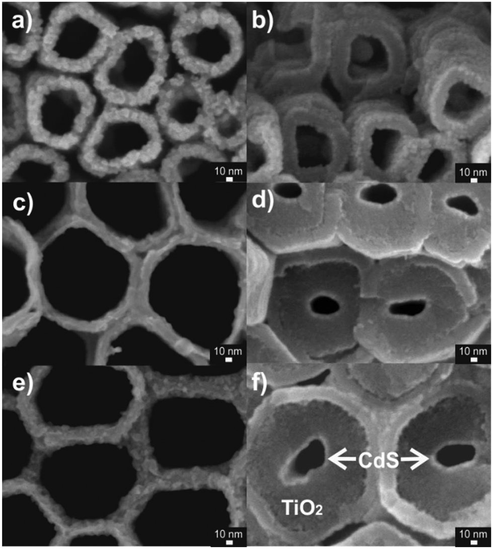 | ||
| Fig. 1 SEM top (a, c, and e) and bottom (b, d, and f) view images of the CdS coated (5 nm) TiO2 nanotube layers of different thicknesses: 1 μm (a and b) 60 μm (c and d) and 130 μm (e and f). | ||
In contrast to the single wall 1 μm thick TiO2 nanotube layers, all the other TiO2 nanotube layers exhibited a double wall structure that is characteristic for the ethylene glycol based electrolytes used for the anodization process.58 However, uniform CdS coating all along the nanotubes was verified through SEM images from the top (Fig. 1a, c and e) and bottom (deepest) parts of the different TiO2 nanotube layers (Fig. 1b, d and f), demonstrating the capability of ALD to uniformly coat thick TiO2 nanotube layers with secondary materials. Further representative SEM images from the top parts of the CdS/TiO2 nanotube layers, along with the corresponding cross-sectional SEM images that verified the thicknesses of the nanotube layers, are shown in Fig. S1.† The thickness of the CdS coating measured from the SEM images (≈ 5.1 ± 0.7 nm, see Experimental section) was in excellent agreement with the thickness value (≈ 5.9 ± 0.2 nm) obtained by ellipsometry measurements of a CdS thin film deposited on Si wafers within the same ALD run.
STEM and EDX analyses were carried out to verify the uniformity of the CdS coatings of the TiO2 nanotube layers as it was achieved in our previous work using other materials.32,33,36,38
Fig. 2a shows a high angle annular dark field (HAADF) scanning transmission electron microscopy (STEM) image of a fragment of a 20 μm thick TiO2 nanotube layer coated with 10 nm of CdS. Therein, one can clearly see the uniform and continuous CdS coating at the interior as well as the exterior part of the TiO2 nanotube. Fig. 2b shows an overall STEM/EDX elemental map. EDX maps of individual elements (namely Cd, S, Ti and O) acquired on fragments of the TiO2 nanotube layer, coated either with 5 nm or with 10 nm of CdS are illustrated in Fig. S2 and S3,† respectively. Finally, Fig. 2c shows the compositional profile of these elements recorded across the line scan (the green line in Fig. 2a and b). In addition, STEM imaging and element mapping were used to verify the coating on a larger scale. Fig. S4 and S5† show the STEM image and EDX maps of a bundle of multiple TiO2 nanotubes coated with 5 nm and 10 nm of CdS, respectively. Overall, analyses in various TEM modes possess a solid verification of the CdS coatings along the tube walls and its corresponding composition.
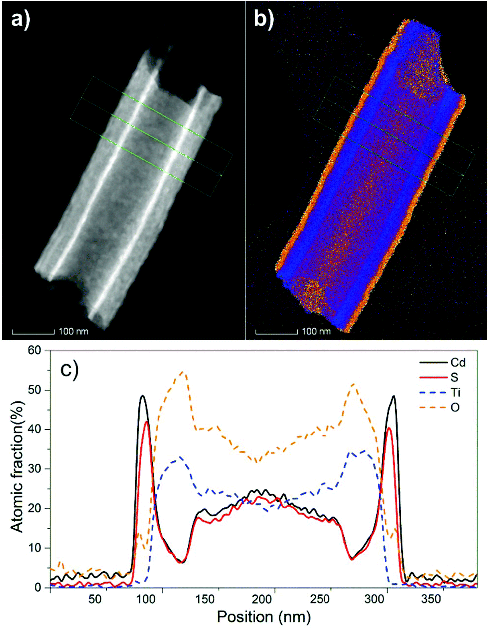 | ||
| Fig. 2 (a) High angle annular dark field (HAADF) scanning transmission electron microscopy (STEM) image and (b) the overall STEM/EDX elemental map of a fragment of a 20 μm thick TiO2 nanotube layer coated with 10 nm of CdS. The green arrow indicates the EDX line scan across the nanotube fragment. (c) The EDX compositional profile corresponding to the line scan. | ||
X-ray photoelectron spectroscopy (XPS) analyses were conducted to determine the chemical composition of the CdS coatings. Fig. 3a illustrates a survey XPS spectra of the CdS coating (20 nm thick) on a Si (100) witness sample, measured in the as deposited state and after a mild sputtering. C and O species were only detected on the surface before sputtering. These impurities were therefore related to sample handling in air following ALD. After sputtering by Ar+ ions, only Cd and S species were visible in the coating. The high-resolution XPS spectrum of Cd and S (Fig. 3b and c) shows the position of the Cd 3d and S 2p peaks at 405.3 eV and 161.5 eV, respectively, which correspond to typical CdS binding energies.59 However, the small shifts of the binding energies of the Cd metal and the Cd oxides and sulphides hinder their differentiation from each other. In order to determine the chemical status of the Cd more precisely, the Auger spectra of the MNN energy levels were acquired (Fig. 3d) and confirmed that the peak at 381.1 eV corresponded to the Cd–S bond.59 Further XPS analyses (shown and discussed later in the text) were carried out to determine the valence band offset between TiO2 and CdS to gain valuable information for a deeper understanding of the photoelectrical behaviour of the coated nanotube layers.
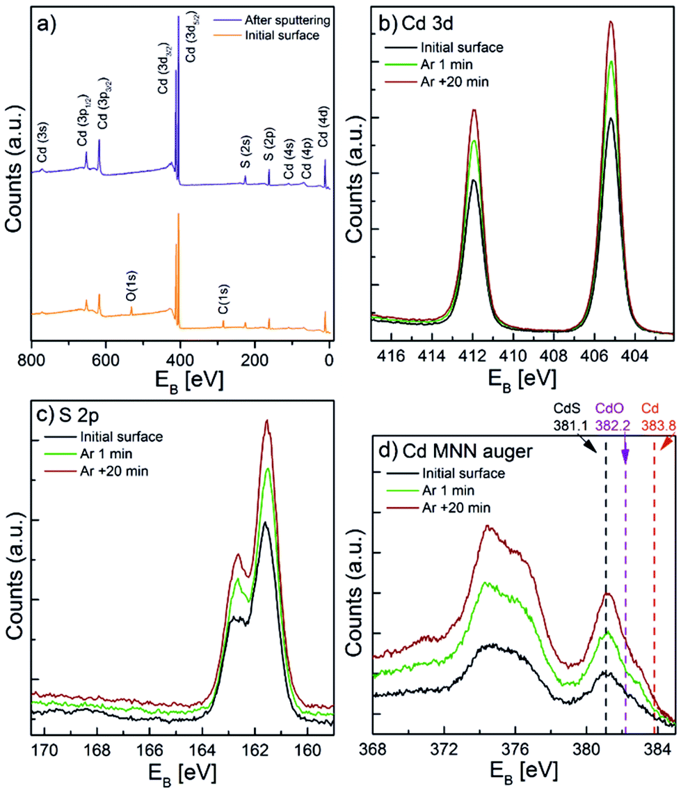 | ||
| Fig. 3 (a) XPS survey spectra of a 20 nm thick CdS film on a Si (100) wafer before and after sputtering. High resolution XPS spectra of (b) Cd and (c) S. (d) Cd MNN Auger spectra. | ||
The crystalline structure of blank and CdS/TiO2 nanotube layers was characterized using X-ray diffractometry (XRD). Fig. 4a and b show the corresponding XRD patterns of 1 μm and 130 μm thick TiO2 nanotube layers (Fig. S6† summarizes the corresponding XRD patterns obtained for all types of TiO2 nanotube layers). The XRD patterns of the blank TiO2 nanotube layers (Fig. 4a and S6†) exhibited the peaks of the metallic Ti substrate, associated with the planes (100), (002), (101) and (102), as well the peaks corresponding to the TiO2 anatase phase planes (101), (004), (200) and (105) of the TiO2 nanotube layers. The XRD patterns obtained for the CdS/TiO2 nanotube layers, illustrated in Fig. 4b and S6,† showed the patterns described for their blank counterparts plus the peaks associated with hexagonal (wurtzite) crystalline CdS planes (002), (101) and (110) with a dominant orientation (002).60Fig. 4c shows a detail of the wurtzite peaks, corresponding to planes (002) and (101), where the intensity of the CdS peaks clearly increased along with the thickness of the TiO2 nanotube layers, indicating a higher CdS loading. Moreover, broad CdS peaks revealed a polycrystalline CdS coating with a small grain size.
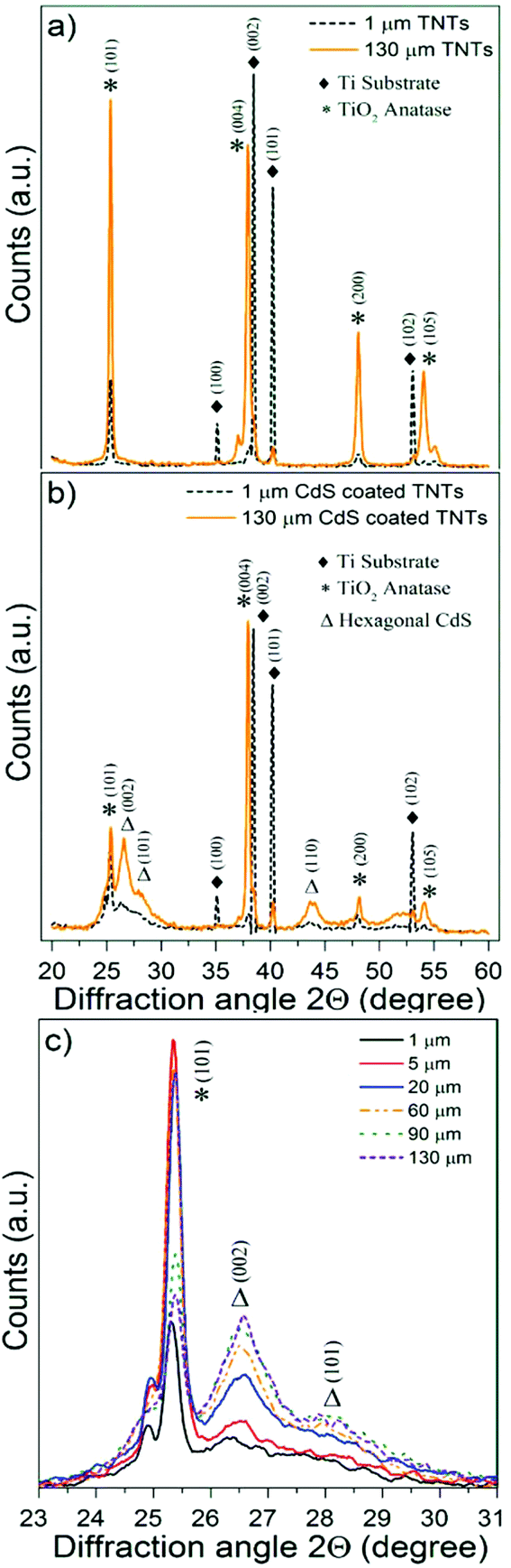 | ||
| Fig. 4 XRD pattern of the (a) blank and (b) CdS coated TiO2 nanotube layers 1 and 130 μm thick. (c) Details of the anatase peak corresponding to the plane (101) and CdS peaks associated to planes (002) and (101) obtained from all the CdS/TiO2 nanotube layers. | ||
Blank and CdS/TiO2 1D conical nanotube layers were further investigated for their photoresponse. Fig. 5 shows the incident photon-to-current efficiency (ICPE) spectra of the blank TiO2 nanotube layers with different thicknesses (Fig. 5a) and their counterpart nanotube layers after CdS coating (Fig. 5b). Blank TiO2 nanotube layers showed no photocurrent in the visible spectral region due to the band gap energy of anatase TiO2Eg ∼ 3.2 eV (≈ 387 nm), while in the UV region the IPCE values were decreasing with increasing thickness of the TiO2 nanotube layers, in line with the literature and as discussed later.61
 | ||
| Fig. 5 (a and b) Incident photon-to-current efficiency and (c and d) transient photocurrent at 360 nm and at 470 nm, respectively, recorded for blank and CdS/TiO2 nanotube layers of different thicknesses. Arrows indicate light ON (↑) and light OFF (↓). (e) Cycling performance of photocurrents transients, measured at 470 nm for 60 μm thick CdS coated TiO2 nanotube layers (21 cycles). | ||
On the contrary, the CdS/TiO2 nanotube layers (Fig. 5b) showed a superior photoresponse in both the UV and visible spectral range. More specifically, their IPCE values were about 3 times higher for the CdS/TiO2 nanotube layers in the UV region (reaching 60–80% IPCE at 360 nm) as compared with the blank TiO2 nanotube layers. The enhancement of the IPCE values in the UV spectral region can be ascribed to the presence of sulphur (S) within the TiO2 nanotube layers which removed TiO2 surface defects and thus inhibited significant charge carrier recombination.19,20,40,62,63 The surface incorporation of S atoms occurred during the very early ALD cycles as the bare TiO2 surface and H2S came into close contact for a significant time (the exposure time was 45 s). The photoresponse of the CdS/TiO2 nanotube layers in the visible spectral region was outstanding as compared to their blank counterparts. The CdS coatings within the nanotube layers caused superior visible light sensitization represented by high IPCE values over a wide range of wavelengths (up to 675 nm). In addition, the IPCE values shown in Fig. 5b were superior to those reported in previous work on TiO2 nanotubes sensitized with CdS by other techniques, regardless of the variety of experimental conditions used for IPCE measurements.23,42–46 We believe this phenomenon stems from the fact that conventional deposition methods lead to decoration of the TiO2 nanotubes by individual particles or particle bundles and hence only affords partial coverage of the TiO2 walls. In contrast, ALD CdS leads to a uniform coating that is in close contact with the entire available surface of the TiO2 nanotubes, and participates then in the light harvesting. The potential of the surface and 1D-architecture of the TiO2 nanotubes is therefore fully exploited, unlike TiO2 nanotubes with particle decoration. Therefore, lower performance of TiO2 nanotubes with particle decoration is understandable.
After all the preliminary tests, a selection of blank (uncoated) nanotube layers as an appropriate reference to their CdS-coated counterparts turned out to be the most suitable for at least three reasons: (i) it is not reasonable to compare the performance of nanotube layers (especially the thick ones, e.g. 130 μm) with mesoporous TiO2 layers of such a thickness due to difficulties for electrons to percolate such a thick porous structure, (ii) the pores of such mesoporous layers are clogged by ALD at the very top of the layer with CdS (yielding low photocurrents, and iii) such comparison was already provided for low aspect ratio nanotube layers by Baker et al.23 and yielded nanotube layers superior to mesoporous layers.
The transient photocurrents of the layers were measured at 360 and 470 nm (Fig. 5c and d), respectively, to obtain additional information about the charge separation within blank and CdS/TiO2 nanotube layers. These wavelengths were selected as they represented (on average) the highest photocurrents achieved for all the layers. Fig. 5c shows that in the UV spectral range, the photocurrent values of the TiO2 nanotube layers increased for 1, 5 and 20 μm thick blank layers, where they reached saturation. In addition, the photoresponse was rather immediate with the light on and off. This is in line with the outcomes of previous reports that showed that nanotube layers with thicknesses of 5–20 μm are the most favourable for efficient performance in the UV spectra range.61,64,65 As further seen in Fig. 5d for thicker layers (60, 90 and 130 μm), the photocurrents decreased with increasing TiO2 nanotube thickness. Moreover, these layers showed very slow responses with the light on and off in contrast to their thinner counterparts (1, 5 and 20 μm). The delayed photocurrent response with the light on and off is clearly due to numerous traps in the nanotube walls, mainly due to surface defects (oxygen vacancies and under-coordinated Ti4+ sites). This phenomenon was already demonstrated in previous literature but never for such a huge span of nanotube layer thicknesses.37,66,67 These features clearly illustrate the strong effect of the TiO2 nanotube layer thickness on the electron transport efficiency. In order to address the stability of the achieved photocurrents, we performed photocurrent transients in numerous cycles with the light “on” and “off”. Fig. 5e shows an example of the photocurrent transients obtained for a 60 μm thick CdS coated TiO2 nanotube layer measured at 470 nm during 21 illumination cycles. As one can see, a minor decay of photocurrent is observed, most likely due to a partial dissolution of CdS in the used electrolyte. However, in a complete solid state cell, such dissolution has no reason to take place, so we consider the stability of the presented CdS coatings and obtained photocurrents as very sufficient.
In order to give a physical description of these results, it is necessary to consider the retrieval length (Lr), defined as the length resulting from adding the electron diffusion length (Ln) and the penetration length (Lλ) of the light at a given wavelength (Lr = Ln + Lλ).61 It is important to note that Lλ is inversely proportional to the absorption coefficient α(λ), which is higher for short wavelengths. The short wavelengths are absorbed at the upper parts of the TiO2 nanotube layers leading to high IPCE values, but it also implies a reduction of the light penetration length Lλ, or eventually shortening Lr. Thus, it could be expected that those TiO2 nanotube layers are thicker than certain Lr values (in this case ≈20 μm) and must experience a detrimental worsening of the electron transport and the photocurrent response. That is, as the electron diffusion distance requires a longer time than the photoelectron lifetime, the electron–hole (e+–h−) recombination probability significantly increases and the photocurrent declines, which is clearly apparent in the case of the 60, 90 and 130 μm layers in Fig. 5a. These results match with the work of Lynch et al.61 who calculated ≈24 μm as the electron diffusion distance within TiO2 nanotube layers synthesized in ethylene glycol.
In contrast, Fig. 5d shows how all the differences in electron diffusion distance were attenuated for the CdS/TiO2 nanotube layers, which is seen from the prompt response with the light on and off and the remarkably enhanced photocurrents for all thicknesses. Such a great photoresponse in the visible spectral region stems from three effects: (i) absorption of the visible light photons in CdS given the bandgap energy of CdS (Eg ≈ 2.4 eV), (ii) the suitable positions of the conduction bands of CdS and TiO2 in the energy diagram allowing for efficient electron transfer of electron,68,69 and (iii) removal of surface defects of the TiO2 nanotubes by CdS leading to a very efficient charge carrier separation. Interestingly, at a wavelength of 470 nm (Fig. 5d), the photocurrents were also highest for the 20 μm thick CdS/TiO2 nanotube layers. This suggests that for this particular thickness, the light absorption and the electron transport within the CdS/TiO2 nanotube layer were optimal (even though all the other layers showed an excellent response too). This means that even the deepest parts of the thickest CdS-coated TiO2 nanotube layers were still involved in efficient electron transport and acted as efficient electron highways.
Another highly significant feature that can be observed for the CdS/TiO2 nanotube layers is the red shift of the IPCE values with increasing thickness of the CdS/TiO2 nanotube layers, as shown in Fig. 5b. For a physical elucidation of the observed red shift, different factors were explored. The first considered factor was the aforementioned content of S within the TiO2 nanotube layers. The S 3p states of the S atoms occupying the substitutional sites are delocalized and can contribute to the valence band (VB) together with the O 2p and Ti 3d states, resulting in an increase of the VB width, and as a consequence a narrowing of the band gap.62,63 Thicker TiO2 nanotube layers exhibited a more prominent red shift that could stem from the higher S content and the more pronounced narrowing of the band gap. Thus, the effect of the incorporated S atoms would be dual: (i) contributing to passivation of the surface defects of the TiO2 nanotube layers (principally the oxygen vacancies), and (ii) narrowing of the optical band gap spreading the absorption to a wider spectral range (i.e. toward longer wavelengths). In line with the content of S, the formation of TiS2 on the TiO2 nanotube surface was also considered. The substitution of S for O was found in the literature to cause a significant shift in the absorption edge to a lower energy and might contribute to the red shift observed.62 However, XPS measurements shown in Fig. S7† did not indicate the presence of TiS2 as only Ti–O bonds were found within the Ti 2p XPS spectra.
The second considered factor was the possible sub bandgap tail of the CdS thin coating within the TiO2 nanotubes. Optical constants of the bulk and thin films of CdS were studied by different authors and most of the works evidenced the existence of a sub bandgap tail (the so called Urbach tail).56,70,71 This tail is responsible for a weak light absorption even for photons with energies lower than the CdS bandgap which is usually believed to be 2.4 eV (≈ 516 nm). The span of the Urbach tail to a lower energy region is characterized by the Urbach energy that can reach values as high as a few hundreds of meV, depending on the method used for the CdS deposition.72 Several suggestions were formulated to assign the presence of the Urbach tail to structural disorder, bulk defects or other as yet undefined inhomogenities in CdS.71–73
To support the discussion of our IPCE results in terms of the possible sub bandgap tail of CdS, we have carried out complementary ellipsometry measurements on planar CdS thin films with a determined thickness of (≈ 5.9 ± 0.2 nm, see Experimental section). These films were deposited onto Si substrates during the same ALD run as was used for the CdS coating of TiO2 nanotubes to keep the deposition conditions of CdS in both cases as close as possible. The obtained spectral dependence of the extinction coefficient of the CdS film is presented in Fig. 6a, where the sub bandgap tail is evident. It is worth mentioning here that for the flat thin CdS film one should expect only a negligible signature of the sub bandgap tail in either the optical reflectance or the transmittance spectra. This is due to relatively low values of absorption coefficients in the CdS tail spectral region and the small thickness of the films (a few nm). However, a significantly different situation could be expected within the 1D conical nanotubular layers and an extremely high surface area of CdS coating on them. In the case of the 1D conical CdS/TiO2 nanotube layers, one can quantify the rather complex light scattering phenomena by the multiple light reflections, absorptions and transmissions in between the tube walls coated by CdS, as schematically depicted in Fig. 6b, whereby the light harvesting ability is enhanced. Similar reflection, scattering and transmittance features were described already for porous alumina.74 The penetration depth of light in the CdS sub bandgap tail spectral region is rather large (about 1 μm) and the TiO2 nanotubes are optically transparent for these wavelengths, therefore it is easy to imagine a huge number of successive transmissions of light through the CdS/TiO2 nanotube walls before the photons escape from the TiO2 nanotube layer as diffuse reflected light or become absorbed inside the CdS/TiO2 nanotube layers. In fact, there are mainly these multiple transmissions, each coupled with small, but not negligible light absorption in the CdS Urbach tail, which results in an effective band gap lowering of the CdS/TiO2 nanotube layer (Fig. 5b). The multiple light scattering with the associated transmission and absorption processes along the nanotubular structure become more pronounced with the increasing thickness of the nanotube layers, as observed in Fig. 5b. In order to support the physical interpretation of this observation, further XPS analyses were carried out to determine the relative positions of the TiO2 and CdS valence and conduction bands at the TiO2/CdS heterojunction. The exact calculations can be found in the ESI (Fig. S8†). The obtained valence band offset value was 1.3 ± 0.2 eV and that implies a conduction band offset value of 0.5 ± 0.2 eV (assuming the band gap energy values of anatase TiO2 and CdS to be 3.2 eV and 2.4 eV, respectively). Therefore, it is evident that the CdS sub bandgap tail (schematically depicted in Fig. 6c) enables the injection of photo-induced electrons into the TiO2 conduction band and this physical scenario fully correlates with our interpretation of an effective band gap lowering based on the optical and IPCE measurements.
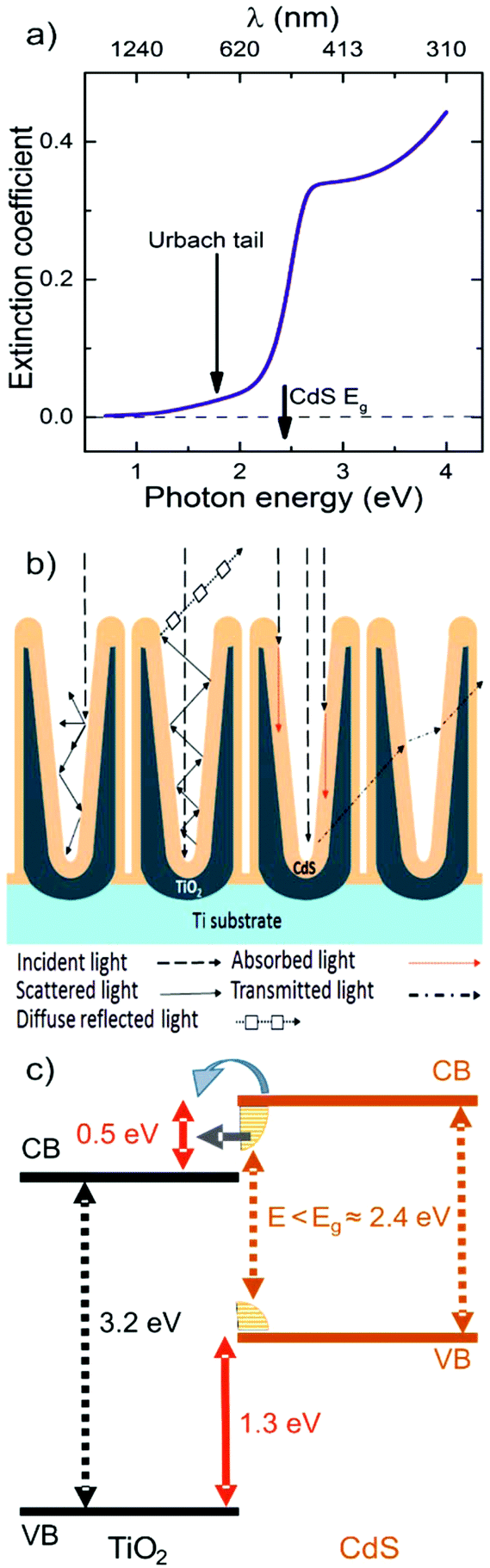 | ||
| Fig. 6 (a) Spectral dependence of the extinction coefficient of CdS, where the solid arrow indicates the sub-band gap tail and the dash dot line the CdS energy band gap (2.4 eV or 516 nm); (b) a simplified sketch illustrating the different interactions of light into the CdS/TiO2 nanotube layers: incident light (long dash line), multi-scattering at different incident light penetration depths (solid line), absorption (red square dot line), transmission (dash dot line) and reflected light (round dot line with white squares); (c) a simplified energy diagram of the valence and conduction energy bands, showing alignment of the CdS/TiO2 junction according to the valence band offsets determined by XPS. The CdS sub bandgap tail allows the photoelectron promotion at a lower energy (E) than the nominal CdS bandgap energy (Eg). | ||
The demonstrated effective band gap lowering has been previously observed and discussed also in the case of CdS/ZnO microplatelets,72 CdS/ZnO nanoporous films,73 and CdS/TiO2 nanotubes with a red shift reported from 516 nm to about 600 nm.52 TiO2 nanorods or nanotubes, regardless of the aspect-ratio, sensitized by CdS in the form of quantum dots, do not show a comparably prominent shift,75–77 probably due to the only partial coverage of the TiO2 walls by the CdS material.
Thus, the most plausible description of the red shift observed in Fig. 5b is a multiple scattering effect of light confined within the 1D conical CdS/TiO2 nanotube layer originating from multiple transmission and absorption processes, without excluding the potential effect of the S content within the TiO2 nanotube layers on the narrowing of the band gap, as previously described. The scattering effect and its impact on the red shift must be directly related to the aspect ratio and the total surface area of the TiO2 nanotube layers, shown in Table 1. Thus, a higher surface and aspect ratio (thicker TNTs) drives to a stronger scattering effect and a noteworthy enhancement of the absorption coefficients in the CdS tail spectral region, triggering a larger red shift of the IPCE values.
The light scattering effect (as an effective means to increase the light harvesting) has been reported for dye sensitized solar cells. Different double layered hierarchical TiO2 structures have been developed containing nanospindles,78 flower shaped structures,79,80 or aggregated TiO2 structures.81,82 Despite the observed significant performance enhancement, they are unfortunately based on complex and tedious fabrication processes. In contrast, herein we present an open conical shaped nanotubular structure (produced using a comparably easier protocol), wherein multiple light scattering effects remarkably enhance the light harvesting. Even though the conical shape of the nanotube layers was previously reported by So et al.83 as highly advantageous for dye sensitized solar cells, that study was limited to 13 μm-thick nanotube layers, the study did not have continuous coatings and did not discuss the multiple scattering phenomena, which are described in this work.
Finally, we studied the photoresponse of the 20 μm thick TiO2 nanotube layers with different CdS coating thicknesses since for this particular thickness, the light absorption and the electron transport within the CdS/TiO2 nanotube layer were found to be optimal as discussed above. The optimal CdS thickness should be such a thickness allowing maximal light absorption within nanotubes while retarding electron–hole recombination. In this way, taking advantage of ALD to precisely control the coating thickness, additional samples of 20 μm thick TiO2 nanotube layers were coated with 17 and 66 ALD cycles to obtain CdS coatings with a nominal thickness of 2.5 and 10 nm, respectively (shown in Fig. S9†), in addition to 5 nm. As shown in Fig. 7a and b, a clear increase of the photocurrent and IPCE values was obtained after increasing the thickness from 2.5 to 5 nm. However, almost identical results were obtained for CdS coating with 5 and 10 nm, despite the diffuse reflectance measurements that showed stronger light absorption for 10 nm thick CdS coatings, as shown in Fig. 7c. These results clearly show that thicker CdS coatings can quantitatively absorb more photons, but they do not produce quantitatively corresponding amounts of electrons. In other words, the lifetime of the photogenerated electrons at the outermost part of the CdS coating is not long enough to successfully reach the TiO2 nanotubes. From this point of view, using a 5 nm CdS coating in this work as the main coating thickness is fully justified and represents the best choice for the optimal photoelectrochemical performance of the CdS/TiO2 nanotube layers.
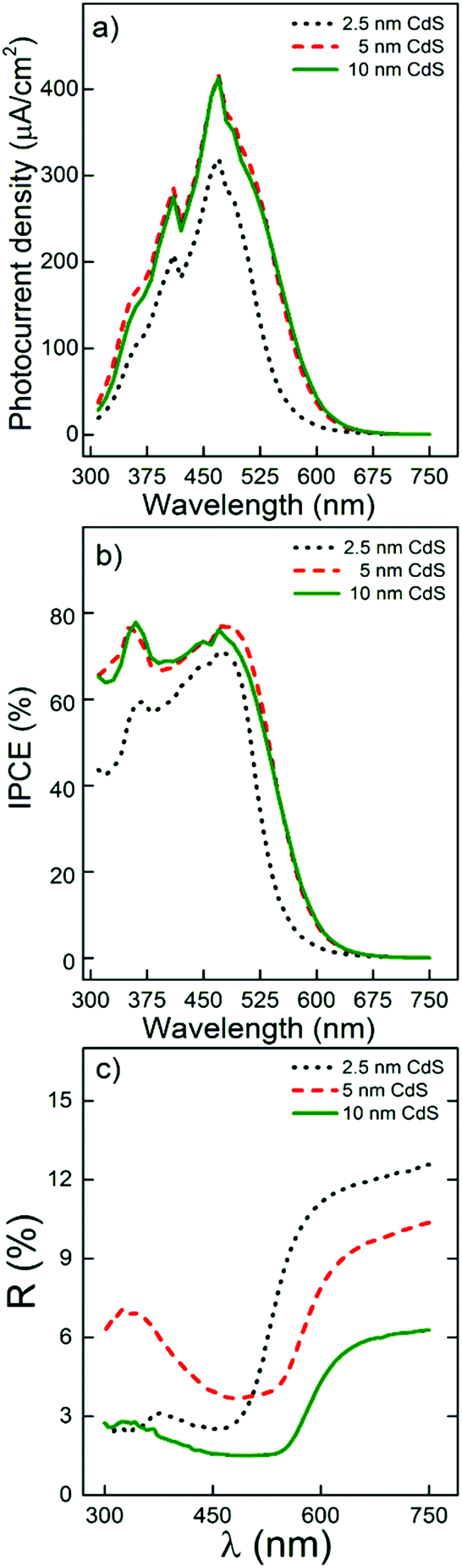 | ||
| Fig. 7 (a) Photocurrent density and (b) incident photon-to-current efficiency recorded for 20 μm thick TiO2 nanotube layers sensitized with different CdS coating thicknesses (2.5, 5 and 10 nm). (c) Diffuse reflectance spectra of TiO2 nanotube layers with a CdS coating of different thickness: 2.5, 5 and 10 nm. | ||
All in all, from the results presented herein it becomes clear that 1D conical TiO2 nanotubes act as effective sinks for photons. The conical nanotube shape has a strong influence on the light absorption profile within the CdS/TiO2 heterostructure and influences the sub bandgap tail of CdS within the TiO2 nanotubes. The results of this work clearly show how effective a strategy it is to deposit suitable secondary materials within the TiO2 nanotube layers by means of ALD to tailor their surface properties and expand the application portfolio of these unique 1D layers. This strategy can be exploited for a whole range of secondary materials with specific functional properties. A whole range of novel solid-state photovoltaic devices (and electrochemical devices in general), which were not feasible before, can be realized using this approach.
Conclusions
In conclusion, we present the superior performance of a 1D conical heterostructured photochemical half-cell based on TiO2 nanotubular scaffolds ALD coated with a thin layer of CdS. The excellent photon-to-electron conversion is a direct consequence of the synergistic effect between the 1D conical nanotubular structure that acts as an electron sink, and the uniform and conformal ALD coating of the CdS light absorber. The resulting high interfacial contact surface area between the scaffold and the light absorber (not achievable otherwise), and the multiple light scattering effects yielded very effective photon absorption and conversion to electrons. We showed that a whole range of nanotube layer thicknesses can be used for this purpose and that the optimal thickness of the absorber coating is approximately 5 nm. This work is a proof of concept for the efficient use of ALD and nanotubular structures for photovoltaic applications. For this purpose, a binary system such as CdS/TiO2 should be considered as a proof of principle tandem. In order to prepare a large scale functional device, promising for future solar cells and other applications, the presented results open up a new pathway to coat TiO2 nanotubes e.g. by kesterites and other functional materials.The door is open to produce a whole range of functional devices, based on the findings presented in this work, including highly efficient solar cells, photocatalytic membranes and catalytic materials.
Conflicts of interest
There are no conflicts to declare.Acknowledgements
The authors gratefully acknowledge support from the European Research Council (ERC, project no. 638857) and the Ministry of Education, Youth and Sports of the Czech Republic (no. LM2015082, LQ1601). The authors acknowledge the CERIC-ERIC Consortium for access to experimental facilities and for financial support under proposal no. 20172101. Dr Katerina Veltruska, Dr Bretislav Smid, Dr Peter Matvija, and Dr Tomas Duchon are acknowledged for their support during XPS measurements. We thank Dr Veronika Podzemna, Mr Jan Michalička and Assoc. Prof. Ludvík Beneš for SEM, HR-TEM and XRD analyses, respectively.Notes and references
- M. A. Green, K. Emery, Y. Hishikawa, W. Warta and E. D. Dunlop, Prog. Photovolt. Res. Appl., 2016, 24, 905–913 CrossRef.
- D. E. Carlson and C. R. Wronski, Appl. Phys. Lett., 1976, 28, 671 CrossRef.
- G. Fulop, M. Doty, P. Meyers, J. Betz and C. H. Liu, Appl. Phys. Lett., 1982, 40, 327 CrossRef.
- H.-W. Schock and R. Noufi, Prog. Photovolt. Res. Appl., 2000, 8, 151–160 CrossRef.
- M. Kaelin, D. Rudmann and A. N. Tiwari, Sol. Energy, 2004, 77, 749–756 CrossRef.
- B. O'Regan and M. Grätzel, Nature, 1991, 353, 737–740 CrossRef.
- U. Bach, D. Lupo, P. Comte, J. E. Moser, F. Weissörtel, J. Salbeck, H. Spreitzer and M. Grätzel, Nature, 1998, 395, 583–585 CrossRef.
- A. Kojima, K. Teshima, Y. Shirai and T. Miyasaka, J. Am. Chem. Soc., 2009, 131, 6050–6051 CrossRef PubMed.
- Z. B. Shao, W. Zhu, Z. Li, Q. H. Yang and G. Z. Wang, J. Phys. Chem. C, 2012, 116, 2438–2442 CrossRef.
- B. Mukherjee, W. Wilson and V. S. Subramanian, Nanoscale, 2013, 5, 269–274 RSC.
- S. Sarker, B. Mukherjee, E. Crone and V. Subramanian, J. Mater. Chem., 2014, A2, 4890–4893 RSC.
- P. Jackson, D. Hariskos, E. Lotter, S. Paetel, R. Wuerz, R. Menner, W. Wischmann and M. Powalla, Prog. Photovolt. Res. Appl., 2011, 19, 894–897 CrossRef.
- A. Walsh, S. Chen, S.-H. Wei and X.-G. Gong, Adv. Energy Mater., 2012, 2, 400–409 CrossRef.
- Y. Itzhaik, O. Niitsoo, M. Page and G. Hodes, J. Phys. Chem. C, 2009, 113, 4254–4256 CrossRef.
- J. M. Macak, H. Tsuchiya, A. Ghicov, K. Yasuda, R. Hahn, S. Bauer and P. Schmuki, Curr. Opin. Solid State Mater. Sci., 2007, 11, 3–18 CrossRef.
- K. Lee, A. Mazare and P. Schmuki, Chem. Rev., 2014, 114, 9385–9454 CrossRef PubMed.
- J. M. Macak, H. Tsuchiya, A. Ghicov and P. Schmuki, Electrochem. Commun., 2005, 7, 1133–1137 CrossRef.
- X. Gao, J. Li, J. Baker, Y. Hou, D. Guan, J. Chen and C. Yuan, Chem. Commun., 2014, 50, 6368–6371 RSC.
- J. M. Macak, T. Kohoutek, L. Wang and R. Beranek, Nanoscale, 2013, 5, 9541–9545 RSC.
- M. Krbal, H. Sopha, V. Podzemna, S. Das, J. Prikryl and J. M. Mack, J. Phys. Chem. C, 2017, 121, 6065–6071 CrossRef.
- Q. Wang, K. Zhu, N. R. Neale and A. J. Frank, Nano Lett., 2009, 9, 806–813 CrossRef PubMed.
- S. Das, H. Sopha, M. Krbal, R. Zazpe, V. Podzemna, J. Prikryl and J. M. Macak, ChemElectroChem, 2017, 4, 1–6 CrossRef PubMed.
- D. R. Baker and P. Kamat, Adv. Funct. Mater., 2009, 19, 805–811 CrossRef.
- Y. Liao, H. Zhang, Z. Zhong, L. Jia, F. Bai, J. Li, P. Zhong, H. Chen and J. Zhang, ACS Appl. Mater. Interfaces, 2013, 5, 11022–11028 CrossRef PubMed.
- T. Suntola, Mater. Sci. Rep., 1989, 4, 261–312 CrossRef.
- C. Detavernier, J. Dendooven, S. P. Sree, K. F. Ludwig and J. A. Martens, Chem. Soc. Rev., 2001, 40, 5242–5253 RSC.
- J. W. Elam, D. Routkevitch, P. P. Mardilovich and S. M. George, Chem. Mater., 2003, 15, 3507–3517 CrossRef.
- J. Bachmann, J. Jing, M. Knez, S. Barth, H. Shen, S. Mathur, U. Gösele and K. Nielsch, J. Am. Chem. Soc., 2007, 129, 9554–9555 CrossRef PubMed.
- S. George, Chem. Rev., 2010, 110, 111–131 CrossRef PubMed.
- K. Jae-Yup, L. Kyeong-Hwan, S. Junyoung, P. Sun Ha, K. Jin Soo, H. Kyu Seok, S. Myung Mo, P. Nicola and S. Yung-Eun, Nanotechnology, 2014, 25, 504003 CrossRef PubMed.
- Q. Gui, X. Zhen, H. Zhang, C. Cheng, X. Zhu, M. Yin, Y. Song, L. Lu, X. Chen and D. Li, ACS Appl. Mater. Interfaces, 2014, 6, 17053–17058 CrossRef PubMed.
- R. Zazpe, M. Knaut, H. Sopha, L. Hromadko, M. Albert, J. Prikryl, V. Gärtnerová, J. W. Bartha and J. M. Macak, Langmuir, 2016, 32, 10551–10558 CrossRef PubMed.
- R. Zazpe, J. Prikryl, V. Gärtnerova, K. Nechvilova, L. Benes, L. Strizik, A. Jäger, M. Bosund, H. Sopha and J. M. Macak, Langmuir, 2017, 33, 3208–3216 CrossRef PubMed.
- H. Cai, Q. You, Z. Hu, Z. Duan, Y. Cui, J. Sun, N. Xu and J. Wu, Sol. Energy Mater. Sol. Cells, 2014, 123, 233–238 CrossRef.
- J.-S. Jeong, B.-H. Choe, J.-H. Lee, J.-J. Lee and W.-Y. Choi, J. Electron. Mater., 2014, 43, 375–380 CrossRef.
- S. Ng, P. Kuberský, M. Krbal, J. Prikryl, V. Gärtnerová, D. Moravcová, H. Sopha, R. Zazpe, F. K. Yam, A. Jäger, L. Hromádko, L. Beneš, A. Hamáček and J. M. Macak, Adv. Eng. Mater., 2017, 19, 1700589 Search PubMed.
- H. Sopha, M. Krbal, S. Ng, J. Prikryl, R. Zazpe, F. K. Yam and J. M. Macak, Appl. Mater. Today, 2017, 9, 104–110 CrossRef.
- J. M. Macak, J. Prikryl, H. Sopha and L. Strizik, Phys. Status Solidi RRL, 2015, 9, 516–520 CrossRef.
- B. Huang, W. Yang, Y. Wen, B. Shan and R. Chen, ACS Appl. Mater. Interfaces, 2015, 7, 422–431 CrossRef PubMed.
- M. Krbal, J. Prikryl, R. Zazpe, H. Sopha and J. M. Macak, Nanoscale, 2017, 9, 7755 RSC.
- X.-F. Gao, W.-T. Sun, Z.-D. Hu, G. Ai, Y.-L. Zhang, S. Feng, F. Li and L.-M. Peng, J. Phys. Chem. C, 2009, 113, 20481–20485 CrossRef.
- M. Qorbany, N. Naseri, O. Moradlou, R. Azimirad and A. Z. Moshfegh, Appl. Catal., B, 2015, 162, 210–216 CrossRef.
- J. Bai, J. Li, Y. Liu, B. Zhou and W. Cai, Appl. Catal., B, 2010, 95, 408–413 CrossRef.
- L. Sang, H. Tan, X. Zhang, Y. Wu, C. Ma and C. Burda, J. Phys. Chem. C, 2012, 116, 18633–18640 CrossRef.
- W.-T. Sun, Y. Yu, H.-Y. Pan, X.-F. Gao, Q. Chen and L.-M. Peng, J. Am. Chem. Soc., 2008, 130, 1124–1125 CrossRef PubMed.
- S. S. Kalanur, S. H. Lee, Y. J. Hwang and O.-S. Joo, J. Photochem. Photobiol., A, 2013, 259, 1–9 CrossRef.
- Y. Yin, Z. Jin and F. Hou, Nanotechnology, 2007, 18, 495608 CrossRef PubMed.
- W. Zhu, X. Liu, H. Liu, D. Tong, J. Yang and J. Peng, J. Am. Chem. Soc., 2010, 132, 12619–12626 CrossRef PubMed.
- S. Banerje, S. K. Mohapatra, P. P. Das and M. Misra, Chem. Mater., 2008, 20, 6784–6791 CrossRef.
- K. Xie, Z. Wu, M. Wang, J. Yu, C. Gong, L. Sun and C. Lin, Electrochem. Commun., 2016, 63, 56–59 CrossRef.
- K. Shin, S. Seok, S. H. Im and J. H. Park, Chem. Commun., 2010, 46, 2385–2387 RSC.
- H. Fu and W. Shen, Nanoscale Res. Lett., 2014, 9, 631 CrossRef PubMed.
- A. Bjelajaca, V. Djokicb, R. Petrovicb, G. Socolc, I. N. Mihailescuc, I. Floread, O. Ersend and D. Janackovic, Appl. Surf. Sci., 2014, 309, 225–230 CrossRef.
- H. Sopha, L. Hromadko, K. Nechvilova and J. M. Macak, J. Electroanal. Chem., 2015, 759, 122–128 CrossRef.
- J. M. Macak, H. Hildebrand, U. Marten-Jans and P. Schmuki, J. Electroanal. Chem., 2008, 624, 254–266 CrossRef.
- L. Ward, in Handbook of optical constants of solids II, ed. E. D. Palik, Academic Press, 1998, pp. 579–596 Search PubMed.
- B. Johs, C. M. Herzinger, J. H. Dinan, A. Cornfeld and J. D. Benson, Thin Solid Films, 1998, 313, 137 CrossRef.
- S. P. Albu, A. Ghicov, S. Aldabergenova, P. Drechsel, D. LeClere, G. E. Thompson, J. M. Macak and P. Schmuki, Adv. Mater., 2008, 20, 4135–4139 Search PubMed.
- D. A. Duncan, J. M. Kephart, K. Horsley, M. Blum, M. Mezher, L. Weinhardt, M. Häming, R. G. Wilks, T. Hofmann, W. Yang, M. Bär, W. S. Sampath and C. Heske, ACS Appl. Mater. Interfaces, 2015, 7, 16382–16386 CrossRef PubMed.
- J. R. Bakke, H. J. Jung, J. T. Tanskane, R. Sinclair and S. F. Bent, Chem. Mater., 2010, 22, 4669–4678 CrossRef.
- R. P. Lynch, A. Guicov and P. Schmuki, J. Electrochem. Soc., 2010, 157, G76–G84 CrossRef.
- T. Umebayashi, T. Yamaki, H. Itoh and K. Asai, Appl. Phys. Lett., 2002, 81, 454–456 CrossRef.
- J. W. Zheng, A. Bhattcahrayya, P. Wu, Z. Chen, J. Highfield, Z. Dong and R. Xu, J. Phys. Chem. C, 2010, 114, 7063–7069 CrossRef.
- I. Paramasivam, H. Jha, N. Liu and P. Schmuki, Small, 2012, 8, 3073–3103 CrossRef PubMed.
- J. M. Macak, A. Ghicov, R. Hahn, H. Tsuchiya and P. Schmuki, J. Mater. Res., 2006, 21, 2824–2828 CrossRef.
- R. Beranek, H. Tsuchiya, T. Sugishima, J. M. Macak, L. Taveira, S. Fujimoto, H. Kisch and P. Schmuki, Appl. Phys. Lett., 2005, 87, 243114 CrossRef.
- H. Tsuchiya, J. M. Macak, A. Ghicov, A. S. Rader, L. Taveira and P. Schmuki, Corros. Sci., 2007, 49, 203–210 CrossRef.
- F. Tian, D. Hou, F. Hu, K. Xie, X. Qiao and D. Li, Appl. Surf. Sci., 2017, 391, 295–302 CrossRef.
- Y.-L. Lee and Y.-S. Lo, Adv. Funct. Mater., 2009, 19, 604–609 CrossRef.
- Z. R. Khan, M. Zulfequar and M. S. Khan, Mater. Sci. Eng., B, 2010, 174, 145–149 CrossRef.
- A. E. Rakhshani and A. S. Al-Azab, J. Phys.: Condens. Matter, 2000, 12, 8745 CrossRef.
- M. V. Malashchonak, E. A. Streltsov, A. V. Mazanik, A. I. Kulak, S. K. Poznyak, O. L. Stroyuk, S. Y. Kuchmiy and P. I. Gaiduk, Thin Solid Films, 2015, 589, 145–152 CrossRef.
- E. Rabinovich and G. Hodes, J. Phys. Chem. C, 2013, 117, 1611–1620 CrossRef.
- A. Brzózka, A. Brudzisz, K. Hnida and G. D. Sulka, in Electrochemically Engineered Nanoporous Materials, Methods, Properties and Applications, ed. D. Losic and A. Santos, Springer Series in Materials Science 220, Switzerland, 2015, pp. 219–233 Search PubMed.
- Y. Xie, G. Ali, S. H. Yoo and S. O. Cho, ACS Appl. Mater. Interfaces, 2010, 10, 2910–2914 CrossRef PubMed.
- C. Chen, L. Ling and F. Li, Nanoscale Res. Lett., 2017, 12, 4 CrossRef PubMed.
- Z. Xie, X. Liu, W. Wang, X. Wang, C. Liu, Q. Xie, Z. Li and Z. Zhang, Nano Energy, 2015, 11, 400–408 CrossRef.
- Y. Qiu, W. Chen and S. Yang, Angew. Chem., Int. Ed., 2010, 49, 3675–3679 CrossRef PubMed.
- F. Shao, J. Sun, L. Gao, S. Yang and J. Luo, ACS Appl. Mater. Interfaces, 2011, 3, 2148–2153 CrossRef PubMed.
- M. Ye, D. Zheng, M. Lv, C. Chen, C. Lin and Z. Lin, Adv. Mater., 2013, 25, 3039–3044 CrossRef PubMed.
- Y. Xiong, D. He, Y. Jin, P. J. Cameron and K. J. Edler, J. Phys. Chem. C, 2015, 119, 22552–22559 CrossRef.
- K. Al-Attafi, A. Nattestad, Y. Yamauchi, S. X. Dou and J. Ho Kim, Sci. Rep., 2017, 7, 10341 CrossRef PubMed.
- S. So, A. Kriesch, U. Peschel and P. Schmuki, J. Mater. Chem. A, 2015, 3, 12603–12608 RSC.
Footnote |
| † Electronic supplementary information (ESI) available. See DOI: 10.1039/c8nr02418a |
| This journal is © The Royal Society of Chemistry 2018 |