
 Open Access Article
 This Open Access Article is licensed under a
 Creative Commons Attribution 3.0 Unported Licence
Towards molecular electronic devices based on ‘all-carbon’ wires†
Andrea
Moneo
a,
Alejandro
González-Orive‡
*ab,
Sören
Bock
c,
Marta
Fenero
ab,
I. Lucía
Herrer
ab,
David C.
Milan
d,
Matteo
Lorenzoni
 e,
Richard J.
Nichols
d,
Pilar
Cea
*ab,
Francesc
Perez-Murano
e,
Paul J.
Low
c and
Santiago
Martin
*af
e,
Richard J.
Nichols
d,
Pilar
Cea
*ab,
Francesc
Perez-Murano
e,
Paul J.
Low
c and
Santiago
Martin
*af
aDepartamento de Química Física, Facultad de Ciencias, Universidad de Zaragoza, 50009, Spain. E-mail: agorive@mail.upb.de; pilarce@unizar.es; smartins@unizar.es
bInstituto de Nanociencia de Aragón (INA) and Laboratorio de Microscopías Avanzadas (LMA), edificio i+d Campus Rio Ebro, Universidad de Zaragoza, C/Mariano Esquillor, s/n, 50018 Zaragoza, Spain
cSchool of Molecular Sciences, University of Western Australia, 35 Stirling Highway, Crawley, WA 6009, Australia
dDepartment of Chemistry, University of Liverpool, Liverpool, L69 7ZD, UK
eInstituto de Microelectrónica de Barcelona (IMB-CNM, CSIC), Campus UAB, 08193 Bellaterra, Spain
fInstituto de Ciencias de Materiales de Aragón (ICMA), Universidad de Zaragoza-CSIC, 50009 Zaragoza, Spain
First published on 27th June 2018
Abstract
Nascent molecular electronic devices based on linear ‘all-carbon’ wires attached to gold electrodes through robust and reliable C–Au contacts are prepared via efficient in situ sequential cleavage of trimethylsilyl end groups from an oligoyne, Me3Si–(C![[triple bond, length as m-dash]](https://www.rsc.org/images/entities/char_e002.gif) C)4–SiMe3 (1). In the first stage of the fabrication process, removal of one trimethylsilyl (TMS) group in the presence of a gold substrate, which ultimately serves as the bottom electrode, using a stoichiometric fluoride-driven process gives a highly-ordered monolayer, Au|CCCCCCCCSiMe3 (Au|C8SiMe3). In the second stage, treatment of Au|C8SiMe3 with excess fluoride results in removal of the remaining TMS protecting group to give a modified monolayer Au|CCCCCCCCH (Au|C8H). The reactive terminal CC–H moiety in Au|C8H can be modified by ‘click’ reactions with (azidomethyl)ferrocene (N3CH2Fc) to introduce a redox probe, to give Au|C6C2N3HCH2Fc. Alternatively, incubation of the modified gold substrate supported monolayer Au|C8H in a solution of gold nanoparticles (GNPs), results in covalent attachment of GNPs on top of the film via a second alkynyl carbon–Au σ-bond, to give structures Au|C8|GNP in which the monolayer of linear, ‘all-carbon’ C8 chains is sandwiched between two macroscopic gold contacts. The covalent carbon–surface bond as well as the covalent attachment of the metal particles to the monolayer by cleavage of the alkyne C–H bond is confirmed by surface-enhanced Raman scattering (SERS). The integrity of the carbon chain in both Au|C6C2N3HCH2Fc systems and after formation of the gold top-contact electrode in Au|C8|GNP is demonstrated through electrochemical methods. The electrical properties of these nascent metal–monolayer–metal devices Au|C8|GNP featuring ‘all-carbon’ molecular wires were characterised by sigmoidal I–V curves, indicative of well-behaved junctions free of short circuits.
C)4–SiMe3 (1). In the first stage of the fabrication process, removal of one trimethylsilyl (TMS) group in the presence of a gold substrate, which ultimately serves as the bottom electrode, using a stoichiometric fluoride-driven process gives a highly-ordered monolayer, Au|CCCCCCCCSiMe3 (Au|C8SiMe3). In the second stage, treatment of Au|C8SiMe3 with excess fluoride results in removal of the remaining TMS protecting group to give a modified monolayer Au|CCCCCCCCH (Au|C8H). The reactive terminal CC–H moiety in Au|C8H can be modified by ‘click’ reactions with (azidomethyl)ferrocene (N3CH2Fc) to introduce a redox probe, to give Au|C6C2N3HCH2Fc. Alternatively, incubation of the modified gold substrate supported monolayer Au|C8H in a solution of gold nanoparticles (GNPs), results in covalent attachment of GNPs on top of the film via a second alkynyl carbon–Au σ-bond, to give structures Au|C8|GNP in which the monolayer of linear, ‘all-carbon’ C8 chains is sandwiched between two macroscopic gold contacts. The covalent carbon–surface bond as well as the covalent attachment of the metal particles to the monolayer by cleavage of the alkyne C–H bond is confirmed by surface-enhanced Raman scattering (SERS). The integrity of the carbon chain in both Au|C6C2N3HCH2Fc systems and after formation of the gold top-contact electrode in Au|C8|GNP is demonstrated through electrochemical methods. The electrical properties of these nascent metal–monolayer–metal devices Au|C8|GNP featuring ‘all-carbon’ molecular wires were characterised by sigmoidal I–V curves, indicative of well-behaved junctions free of short circuits.
Introduction
The realisation of molecular-scale electronic devices requires the development of suitable molecular components that can perform a range of electronic functions, possibly combined into larger, more highly functional molecular assemblies, and ultimately connected to a macroscopic support to allow integration into a solid-state platform.1–3 When considering the different components needed to form a ‘molecular electronics kit’ for fabrication of functional devices, molecular wires are regarded as the most fundamental.4–6 Molecular wires typically feature a rigid linear molecular backbone, and π-conjugated electronic structure that can facilitate electron transport.7,8 A host of molecular structures of varying degrees of complexity that meet these general design criteria have been proposed to serve as wire-like molecules and investigated using a wide range of experimental, computational and theoretical methods.8Of the various π-conjugated molecules that can be conceived to serve as molecular wires, linear chains of sp-hybridised carbon with cumulated (![[double bond, length as m-dash]](https://www.rsc.org/images/entities/char_e001.gif) CCCC) or polyynyl (–CC–CC–) structures have attracted considerable attention,9–18 and in more recent times the challenges and electronic features that arise when such carbon chains are contacted to two electrode surfaces have been discussed. Such linear arrays of sp-hybridised carbon atoms with alternating single and triple bonds or cumulated structures offer an approximately cylindrical distribution of electron density along a one-dimensional, rigid-rod, length-persistent backbone.19–21 In contrast, more commonly employed structures used in the construction of wire-like molecules based on oligomeric(phenylene ethynylene) (OPE) structures feature interpolated phenylene rings,22–27 and whilst the barrier to rotation of the phenylene ring around the long molecular axis is low28,29 conjugation is interrupted when the phenyl rings are rotated with respect to each other and the resulting wires offer only moderate performance with decay constants β ca. 2 nm−1 (G ∝ e−βrG0).30 However, creating experimental platforms to explore these concepts remains a substantial challenge.31–41 In seeking to introduce analogues of sp-hybridised carbon chains into molecular junctions, attention has naturally turned to oligoynes capped by suitable surface binding groups as model systems.16,42–45 These systems have revealed promisingly high conductance and, under optimal conditions and solvent environments, low β values (ca. 0.1–1 nm−1), indicating considerable promise as wire-like components.
CCCC) or polyynyl (–CC–CC–) structures have attracted considerable attention,9–18 and in more recent times the challenges and electronic features that arise when such carbon chains are contacted to two electrode surfaces have been discussed. Such linear arrays of sp-hybridised carbon atoms with alternating single and triple bonds or cumulated structures offer an approximately cylindrical distribution of electron density along a one-dimensional, rigid-rod, length-persistent backbone.19–21 In contrast, more commonly employed structures used in the construction of wire-like molecules based on oligomeric(phenylene ethynylene) (OPE) structures feature interpolated phenylene rings,22–27 and whilst the barrier to rotation of the phenylene ring around the long molecular axis is low28,29 conjugation is interrupted when the phenyl rings are rotated with respect to each other and the resulting wires offer only moderate performance with decay constants β ca. 2 nm−1 (G ∝ e−βrG0).30 However, creating experimental platforms to explore these concepts remains a substantial challenge.31–41 In seeking to introduce analogues of sp-hybridised carbon chains into molecular junctions, attention has naturally turned to oligoynes capped by suitable surface binding groups as model systems.16,42–45 These systems have revealed promisingly high conductance and, under optimal conditions and solvent environments, low β values (ca. 0.1–1 nm−1), indicating considerable promise as wire-like components.
Recently it has become possible to directly contact alkyne moieties to metal surfaces, M, through M|CCR linkages either by direct reaction of terminal alkynes, RCCH, with gold nanoparticles,46 or surfaces,47–49 or from RCCSiMe3 or RCCSiiPr3 moieties via in situ removal of a trimethylsilyl or triisopropylsilyl protecting group upon treatment with fluoride.50–52 Such desilylation chemistry can therefore be applied in situ to directly attach a carbon chain to gold via a suitably functionalised oligoyne, Me3Si–(CC)n–SiMe3. We report here for the first fabrication of two terminal sandwich-based devices Au|CCCCCCCC|Au, with the C8 fragment being introduced through sequential desilylation/metallation of the trimethylsilyl-protected octa-1,3,5,7-tetrayne, Me3Si–(CC)4–SiMe3 (1, Fig. 1) with the formation of an Au–C σ-bond both at the bottom and at the upper electrode. In this approach, a stable, uniform and highly ordered Au|CCCCCCCCSiMe3 (Au|C8SiMe3) monolayer was initially fabricated by using desilylation chemistry of the oligoyne end-capped by SiMe3 groups with the formation of an Au–C σ-bond. In a subsequent step, treatment of Au|C8SiMe3 with excess fluoride results in removal of the remaining SiMe3 protecting group to give the modified monolayer Au|CCCCCCCCH (Au|C8H). The upper electrode was finally fabricated by the incubation of the modified surface in a dispersion of unprotected gold nanoparticles (GNPs), resulting in chemisorption of GNPs to the monolayer through Au–C bonds to give robust sandwich-like device structures Au|CCCCCCCC|GNP (Au|C8|GNP) in an experimentally simple fashion. Electrochemical and electrical measurements on these structures confirm the reproducibility of the fabrication approach, which is achieved without formation of metallic filaments through the carbon monolayer or other short circuits. Thus, the sequential desilylation/metallation strategy allows the simple fabrication of sandwich-like device structures of uncapped carbon chains, opening new avenues to their wider exploration and exploitation in molecular electronics.
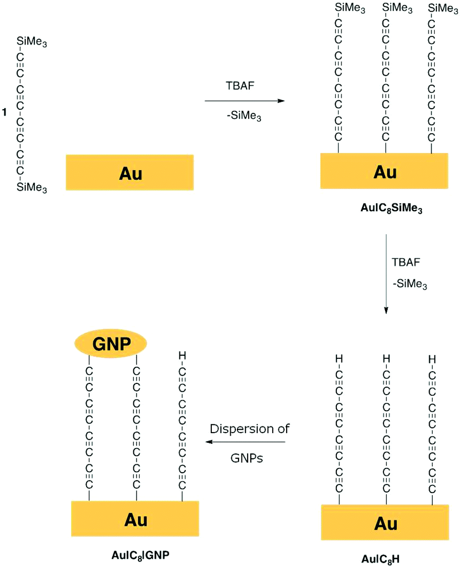 | ||
| Fig. 1 A schematic representation of the procedure followed to form two terminal sandwich-based metal–organic monolayer–metal devices (Au|C8|GNP) by Au–C covalent bonds via sequential in situ desilylation of a trimethylsilyl-protected octatetrayne, 1, and surface functionalisation by incubation of the monolayer modified substrate in a dispersion of unprotected gold nanoparticles (GNPs). | ||
Results
Fabrication of an Au|C8H film
A Au(111) surface was modified by the formation of a gold–carbon (Au–C) covalent bond via in situ desilylation of the bis(trimethylsilyl)-protected octatetrayne Me3Si–(CC)4–SiMe3 (1) using equimolar tetrabutylammonium fluoride (TBAF, Fig. 1).50,53 In this first stage, a freshly annealed gold electrode was immersed in a freshly prepared THF solution of 1 (1 mM) containing equimolar TBAF and incubated for 10 min at room temperature. The electrode was then rinsed copiously with THF to remove any physisorbed species, and dried under a nitrogen flow, to give a monolayer film Au|C8SiMe3. In a second stage, the modified surface was immersed in a THF solution of TBAF (0.05 M) at room temperature for 30 min, before being thoroughly rinsed with THF and dried. Under this experimental procedure, the distal trimethylsilyl (TMS) groups on the monolayer modified electrode are cleaved to give an Au|C8H film (Fig. 1 and S1 in the ESI†). These procedures gave highly-ordered, chemically well-defined monolayers on the well-ordered Au(111) surface, which were characterised by quartz-crystal microbalance (QCM), atomic force microscopy (AFM) imaging and depth profiling, and Raman spectroscopy as described below.
The monolayer thickness in the Au|C8SiMe3 films was determined by the atomic force microscopy (AFM) scratching technique, which involves ploughing the organic film with the AFM tip in contact mode and then imaging across the scratch to measure the depth profile (Fig. S2†). A film thickness of 1.0 ± 0.2 nm was estimated from this technique which is in good agreement with the estimated Au⋯Si distance from an Au–CCCCCCCCSiMe3 computational model (1.3 nm). As illustrated in the schematic depicted in Fig. 1, the maximum surface coverage of the polycarbon chain will be limited by the size of the SiMe3 protecting group, which determines the separation between adjacent molecules in the Au|C8SiMe3 monolayer film. Assuming a close/hexagonal packing arrangement of molecules within the monolayer, along with equivalent surface area occupied by the protecting SiMe3 group (treated as a model disk with a diameter of 0.758 nm),54 a theoretical maximum coverage of C8SiMe3 fragments on an Au(111) surface can be calculated, resulting in a value of 3.34 × 10⁻¹⁰ mol cm−2.54 To estimate the surface coverage experimentally, the variation in the resonator frequency of a quartz crystal microbalance (QCM) substrate before and after the formation of Au|C8SiMe3 was recorded as described in the ESI.† The resulting experimental surface coverage for the monolayer on gold was determined to be 3.13 × 10⁻¹⁰ mol cm−2, in good agreement with the theoretical maximum surface coverage. The incubation of a QCM resonator in a 1.0 × 10⁻³ M solution of 1 in THF without TBAF did not show any frequency change, which indicates that a desilylation of the trimethylsilyl-protected oligoyne with TBAF is mandatory in order to form a robust monolayer of 1 on a gold substrate. This is in contrast with the more stable monolayer films formed from long chain hydrocarbon substituted trimethylsilylacetylene derivatives.55–58
Several earlier studies also describe the formation of a covalent Au–C σ-bond upon removal of the trimethylsilyl (TMS) group attached to an alkynyl moiety,50–52 and here Raman spectroscopy and surface enhanced Raman spectroscopy (SERS) studies were also carried out to further support the proposed formation of a metal–carbon bond at the substrate surface. The Raman spectrum of a powder sample of 1 (Fig. 2a) is characterised by intense bands near 2140 cm−1 which can be attributed to the symmetric ν(CCCC) band of the innermost C4 atoms (calculated 2270 cm−1) and the coupled symmetric stretches of the CC(SiMe3) moieties (calculated 2210 cm−1). Much weaker CH bend (calculated 1503 cm−1) and ν(Si–CH3) (calculated 586 cm−1) bands are also observed.
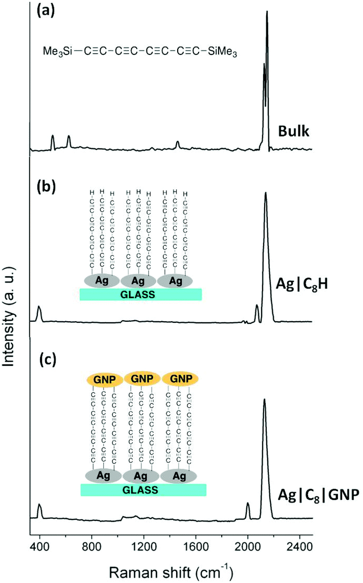 | ||
| Fig. 2 (a) Raman spectrum of a powder sample of 1; (b) SERS spectrum of an Ag|C8H film; and (c) SERS spectrum of an Ag|C8|GNP film. | ||
Raman scattering is dramatically enhanced by surface effects, which are particularly pronounced on rough silver surfaces,59–61 offering a convenient avenue through which to assess the surface chemistry following desilylation of 1, albeit on model silver surfaces rather than Au(111) substrates. Similar studies of the desilylation/surface-C bond forming process on Au, Pt, Pd, HOPG51 and Ag46 surfaces using phenylene ethynylene derivatives have been reported elsewhere by others. Silver islands of thickness 9.1 nm were deposited on glass slides by thermal evaporation and these served as SERS substrates. In a manner entirely analogous to the process depicted in Fig. 1, these silver mirrored slides were immersed in a freshly prepared THF solution of 1 (1 mM) containing equimolar TBAF and incubated for 10 minutes at room temperature, rinsed copiously with THF and dried, to give Ag|C8SiMe3 modified substrates. The slide was then immersed in a THF solution containing excess fluoride to give Ag|C8H modified surfaces. The resulting SERS spectrum of the Ag|C8H substrates shows strong ν(CC) bands near 2140 cm−1, albeit with less resolution than the powder sample, indicating that the oligoyne chain remains intact after being grafted on the surface. The disappearance of the vibrational bands associated with the SiMe3 moieties as well as the appearance of an additional weak ν(CCH) band at 2081 cm−1, due to the terminal CCH group confirms desilylation of the silyl-protected oligoyne. Critically, the appearance of a new band at 397 cm−1, which is characteristic of a metal–C stretching mode (with the metal being Au, Ag, or Pd) is the most direct evidence for the formation of a M–C σ-bond.50,51,62
To further confirm the removal of the trimethylsilyl moieties and formation of a terminal alkyne (–CCH) functionalised surface through this desilylation/surface coordination/desilylation sequence from 1, click chemistry reactions were employed to further develop Au|C8H films.47,54,63–65 An Au|C8H monolayer film was incubated in a solution of (azidomethyl)ferrocene (N3CH2Fc) to incorporate an electroactive ferrocene head-group to the monolayer via a copper catalyzed azide–alkyne (CuCAA) click reaction (Fig. 3a).54,66,67 The resulting Au|C6C2(H)N3CH2Fc films were studied by cyclic voltammetry (Fig. 3b at 200 mV s−1 scan rate) revealing characteristic ferrocene/ferrocenium couple with a peak-to-peak separation ΔEp = 110 mV. Although this is a substantial peak separation for such an immobilised redox species, it is nevertheless in good agreement with similarly constructed ferrocene-functionalised 1,4-diethynylbenzene monolayers on Au(111).47 The relatively broad voltammetry wave might arise from disorder of the ferrocene head-groups across the surface of the oligoyne film.68,69 The peak current of both the oxidative and the reductive waves display linear dependence on potential scan rate (Fig. 3c and S3†) clearly indicating surface-bound ferrocene molecules. From the relationship Γ = Q/nFA, where Q is the total charge estimated from integration of the oxidation wave in the I–V plot, n is the number of electrons transferred per molecule (1 in the case of ferrocene/ferrocenium couple), F is the Faraday constant and A is the effective electrode area, an experimental ferrocene surface coverage of 5.54 × 10⁻¹¹ mol cm−2 is obtained. This ferrocene surface coverage, which is approximately an order of magnitude lower than that estimated for the Au|C8H base layer (see above), is similar to the estimates obtained by Pla-Vilanova et al. from a copper catalyzed azide–alkyne click-modified SAM of 1,4-diethynylbenzene.47
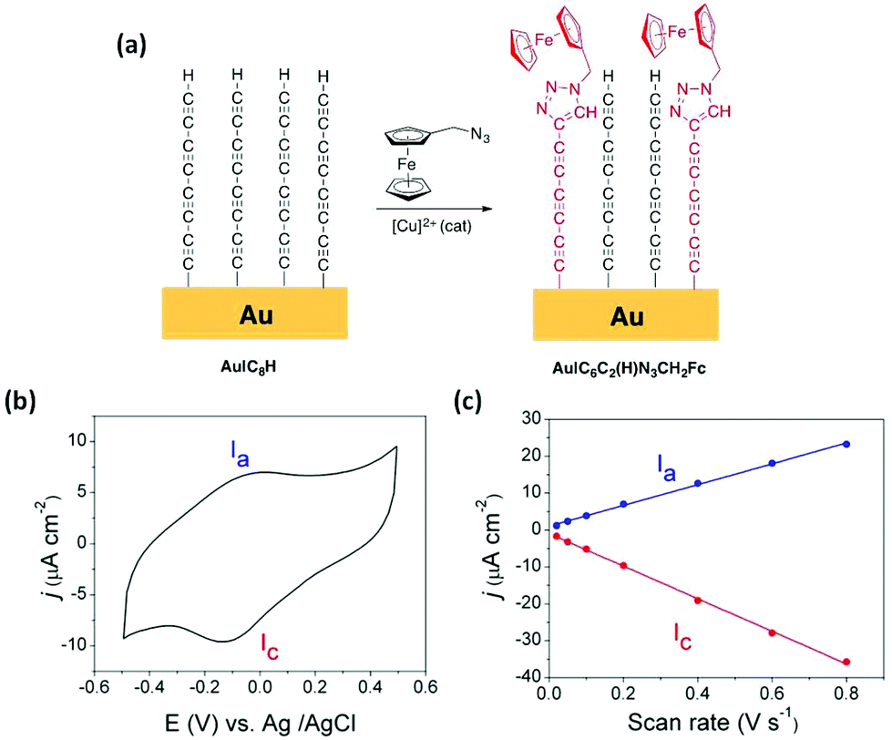 | ||
| Fig. 3 (a) Scheme of the click chemistry reaction (CuCAA) to form an Au|C6C2(H)N3CH2Fc film. (b) Cyclic voltammogram recorded for an Au|C6C2(H)N3CH2Fc film in 1-hexyl-3-methylimidazolium hexafluorophosphate (HMIm-PF6) ionic liquid at a scan rate of 200 mV s−1. (c) Scan rate-dependent peak currents for the anodic Ia and cathodic scans Ic and their linear fitting. | ||
The introduction of a redox-active ferrocene moiety also allows an estimation of the standard heterogeneous rate constant, kET, between the chemisorbed ferrocene groups and the underlying Au(111) electrode using the Laviron analysis (Fig. S3†).70,71 The resulting kET was 3.2 ± 0.1 s−1, which is similar to values obtained from ferrocene-terminated peptide nucleic acid (PNA) SAMs of similar thickness (kET ∼3 s−1).72 It is relevant to note that these peptide nucleic acid (PNA)-based SAMs are known to exhibit high conductance values,73,74 and therefore reasonably efficient ET between the underlying electrode surface and the distal ferrocene groups through the polyyne chain can be inferred.
Fabrication of a top-contact electrode
Modified substrates Au|C8H were incubated in a dispersion of freshly prepared ligandless gold nanoparticles (GNPs) (Fig. 1). The hydrodynamic diameter of the as prepared GNPs in solution was found to be in the 7–28 nm range, as determined by Dynamic Light Scattering, DLS (see Experimental section). This rather broad distribution gives some indication of aggregation of the bare GNPs in solution. The deposition time (3 h) of these particles on the Au|C8H substrate was optimised via QCM methods by following the resonator frequency (coupled to increases in mass) until a constant value was obtained (Fig. S4†). Immediately after the removal of the substrates from the incubation solution the films were thoroughly rinsed with Milli-Q water to eliminate physisorbed GNPs from the film surface, and were allowed to dry, giving Au|C8|GNP assemblies. Similar methods were used to prepare Ag|C8|GNP bimetallic structures. The observation of the ν(M–C) band envelope at ca. 399 cm−1 (Fig. 2c) is consistent with the formation of M–C σ-bonds, although the individual ν(Ag–C) and ν(Au–C) bands could not be distinguished from each other within the resolution of the SERS spectrum. The functionalisation of the terminal ethynyl motif is further supported by the absence of the ν(CCH) band, whilst the appearance of a new, lower frequency ν(CCAu) band at 2000 cm−1 is consistent with the functionalisation of the surface by GNPs.46,50,51
Imaging of the surface by AFM was used to obtain information about the distribution, shape and size of the GNPs on the surface of the film. AFM images of Au|C8H show a highly ordered monomolecular layer (Fig. 4). In contrast, after incubation in the dispersion of GNPs, AFM images of the Au|C8|GNP film (Fig. 4) show the appearance of raised surface features, with average diameter of 24.6 ± 5.2, and average height of 6.5 ± 1.5 nm, resulting in an increase in the RMS (root-mean-square roughness) from 0.41 to 1.43 nm and clearly revealing the presence of GNPs on-top of the surface film (Fig. 4, S5, and S6†). Using a statistical analysis of the data extracted from height profiles across AFM images as depicted in Fig. S6,† individual features are in the 10–35 nm range in lateral width and the 4–12 nm range in height. The size distribution of these surface features compares with the 7–28 nm range of particle sizes determined for the initial dispersions and suggests that there is a small degree of additional aggregation on the film surface. A bearing analysis of the AFM images (Fig. S7†) was made, giving an estimated surface coverage of 40%, in good agreement with the gold nanoparticle surface coverage exhibited by a SAM of 1,4-diethynylbenzene on Au(111).75
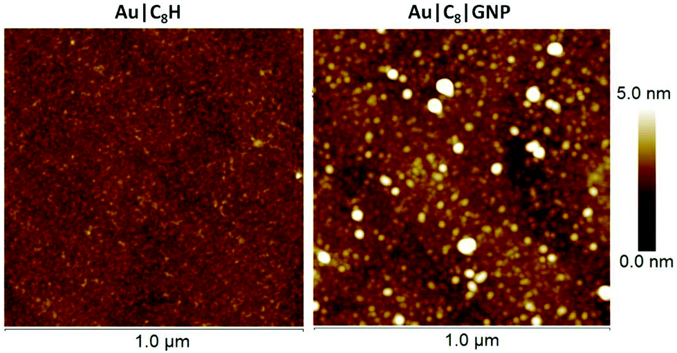 | ||
| Fig. 4 AFM images of (left) an Au|C8H film and (right) after incubation for 3 hours in a dispersion of GNPs to form an Au|C8|GNP film. | ||
Electrochemical behavior of Au|C8H
These film-modified gold substrates were used as working electrodes in cyclic voltammetry measurements with the aim here being to characterise the electrochemical stability exhibited by the as-prepared Au|C8H films. In these cyclic voltammetry measurements both the electrochemical reductive (in 0.1 M NaOH) and oxidative (in 0.1 M HClO4) properties of the assembled monolayer were assessed, with pH being used to control the competing water redox chemistry. On the oxidation sweep in 0.1 M HClO4, an anodic voltammetric peak at 1.40 V corresponding to an oxidative current peak (Poxi) is observed (Fig. 5a). The substantial electrochemical current involved in this process is attributed to both the electrochemical oxidation of the carbon chain and to the formation of a gold oxide surface layer. By integrating the relevant peaks, the electrochemical charge involved in the oxidative electro-desorption peak, (Poxi) in Fig. 5a is obtained. By then subtracting the anodic charge recorded in the second cycle (corresponding to the gold oxide formation contribution), a surface charge density of 1400 μC cm−2 is estimated. This is a substantial charge, consistent with a multi-electron process associated with oxidation of the carbon chain, but as the stoichiometry of the oxidation process is unknown, the charge density cannot be used to quantify the surface coverage. Significant contributions over the last few years have shown that both aliphatic and aromatic ethynyl-terminated molecules give rise to SAMs on Au(111) surfaces which can be considered as analogous to thiol-terminated molecules in terms of surface coverage and electrochemical behavior.51,75,76 In this regard, the afore-mentioned value, i.e. 1400 μC cm−2, is nearly twice as much that exhibited by SAMs of alkanethiols,77 but analogous to that shown by dithiols.78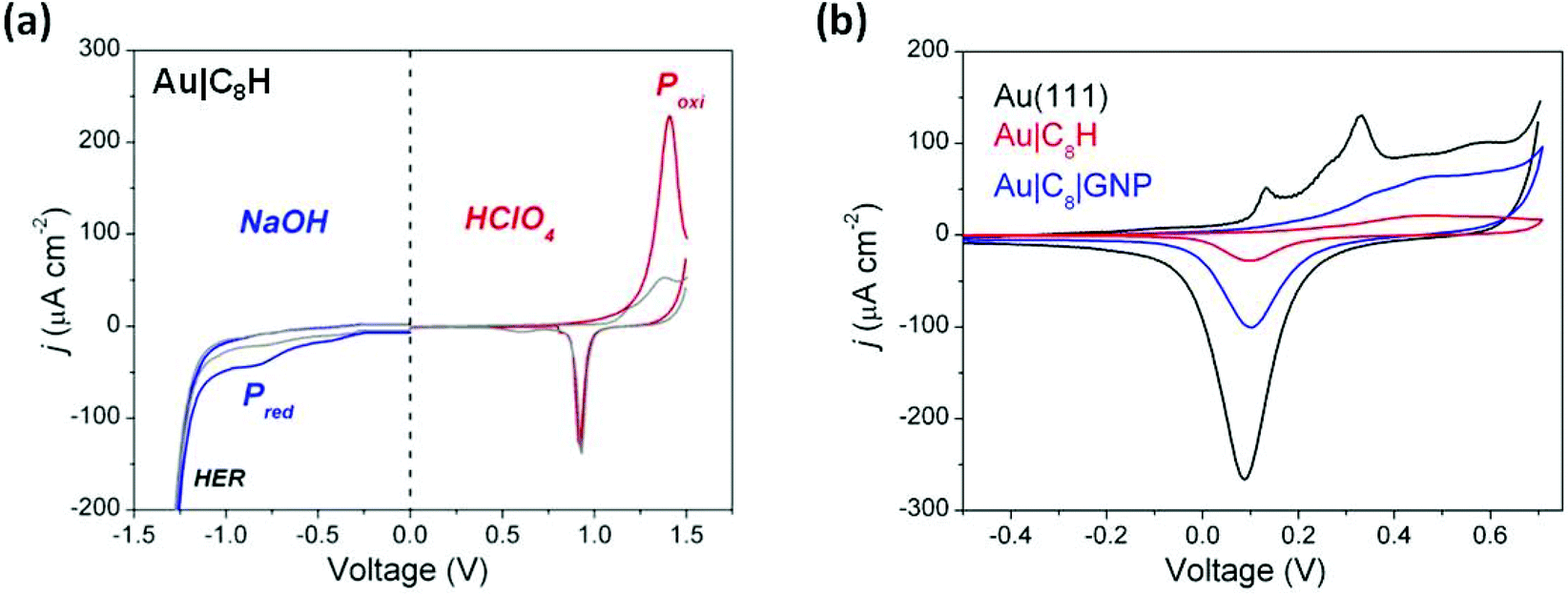 | ||
| Fig. 5 (a) Cyclic voltammograms for Au|C8H in aqueous electrolyte of 0.1 M NaOH (blue curve, left half panel) and 0.1 M HClO4 (red curve, right half panel) at a scan rate of 10 mV s−1. The blue and red curves indicate the first potential cycle and the grey curves represent the subsequent second cycle. Current peaks corresponding to oxidative and reductive processes of the carbon chain are identified as Poxi and Pred, respectively. (b) Cyclic voltammograms recorded for a bare Au(111), Au|C8H and Au|C8|GNP in 0.1 M NaOH at 100 mV s−1. The reference electrode was Ag|AgCl, KCl 3 M. | ||
On the other hand, a broad cathodic peak at −0.85 V (Pred) was observed when a 0.1 M NaOH solution was used (Fig. 5a). This precedes the hydrogen evolution reaction (HER) and is associated with the reductive processes of the surface film. The electrochemical charge involved in this reduction peak for Au|C8H was estimated as 27 μC cm−2. If the peak is assumed to be a cathodic electro-desorption of the carbon chain following a single electron process then surface coverage can be estimated. With these assumptions and using Γ = Q/nFA, an experimental surface coverage of 2.84 × 10⁻¹⁰ mol cm−2 is obtained. This value is in reasonably good agreement with the experimental surface coverage determined by using a QCM (3.13 × 10⁻¹⁰ mol cm−2) supporting the notion that the reductive peak corresponds to a 1 electron process. Taken together, the oxidation and reduction electrochemical results define a workable potential window of 2.25 V, which is similar to that reported for thiol-based organic molecules assembled on gold surfaces79 as well as for ethynyl-terminated aryl moieties.51
Finally, additional cyclic voltammetry (CV) measurements involving a bare Au(111), Au|C8H and Au|C8|GNP structures were carried out in 0.1 M NaOH (Fig. 5b). The electrochemical behavior of the unmodified Au(111) electrode exhibits the typical sharp peaks at 0.13 and 0.33 V, associated with the gold oxide formation, and the subsequent electro-reduction in the cathodic scan.80,81 After modifying the Au(111) surface with Au|C8H, electrochemical formation of the gold oxide monolayer is suppressed as shown by the much smaller current. This suggests a rather effective blocking behaviour of the hydrophobic carbon chain to the OH− ions and water molecules which are required to form the gold oxide. The small current flow in this case points to relatively few defects/pinholes in the monolayer. Once the GNPs are assembled to give the Au|C8|GNP sandwich structures, the resulting voltammogram exhibited the formation and reduction of the gold oxide monolayer, but with the typical non-peaked featureless profile corresponding to polycrystalline gold nanoparticles.82,83 Consequently, this observation is unlikely to arise from diffusion of OH− ions and water molecules through defects or pinholes in the organic layer, but it is associated with the electrochemical response of the attached GNPs. This further confirms that GNPs adsorption does not cause significant damage to the organic layer.
Electrical characteristics of Au|C8|GNP
At this point it is crucial to verify that the metal-contacting strategy proposed does not result in short-circuits by penetration of GNPs into the monolayer and also to determine the electrical characteristics of these metal–monolayer–GNP assemblies. To do so, I–V curves were recorded for these Au|C8|GNP structures using a conductive atomic force microscope (c-AFM; Bruker ICON) with the PeakForce tunneling AFM (PF-TUNA) mode.46,84–87 Under these conditions, the tip makes intermittent contact with the surface at a frequency of 2 kHz and a low maximum force (peak-force) to limit damage to the surface and detrimental lateral forces. Therefore, the peak-force tapping mode is a valuable method for conductivity mapping of delicate samples since it avoids lateral forces that may otherwise damage the tip coating and the soft sample surface. Nevertheless, before recording the I–V curves, a compromise has to be made in order to select the most suitable contact force to be applied during the measurement taking into account that the set-point force suffers from 8% uncertainty due to the calibration method (thermal tuning).88 This compromise involves applying peak forces during the measurements that are not so great as to result in large deformation of the monolayer underlying the GNPs, but also to avoid applying too little force which would result in an inadequate contact between the tip and the surface, leading to ineffective electrical probing. This latter point is illustrated in Fig. 6a, which shows how an increase in the applied force results in a more effective contact between the tip and the GNPs. The conductance value was obtained as the slope of the linear fitting of the experimental data from −0.5 to 0.5 V, the ohmic region, from the average I–V curve collected at each set-point force. When a set-point force below 3 nN was used, no current was detected, whilst for a set-point force between 3 and 6 nN a low conductance value was obtained. These data show that when low set-point forces are applied, the contact between the tip and the GNP results in practically no measurable electrical current flow. Meanwhile, when higher set-point forces are applied (between 9 and 18 nN), a significant conductance value is obtained, confirming that for these set-point forces there is a good electrical contact. In addition, a log–log plot of junction conductance versus the applied set-point force (Fig. S8†) shows that the increasing conductance with set-point force follows a single power law dependence (i.e., log (conductance) ∝ log (set-point force)·n with n = 3.56) for the set-point force range exhibiting a significant conductance (between 9 and 18 nN).89 From these observations it is concluded that 9 nN is the minimum set-point force required to make a reasonable contact between the tip and the GNP.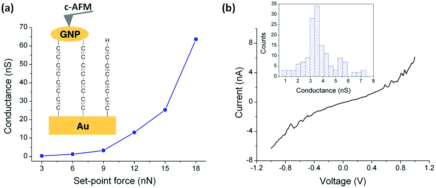 | ||
| Fig. 6 (a) Average conductance values measured by locating the tip of the c-AFM on top of GNPs at the indicated set-point forces. Inset: A scheme of the Au|C8|GNP structures contacted by the c-AFM tip. (b) Representative I–V curve experimentally obtained by positioning the c-AFM tip on top of a GNP when a set-point force of 9 nN was applied. Inset: Conductance histogram built by adding all the experimental data from −0.5 to 0.5 V for each I–V curve obtained (ca. 150 curves). | ||
With the influence of the applied set-point force on the monolayer established, I–V curves were recorded by locating the AFM tip on top of GNPs (Fig. 6a). To ensure reproducibility and reliability of the results, the I–V curves at each set-point force were averaged from multiple scans which were recorded by locating the AFM tip on top of different GNPs with approximately the same size (ca. 20 nm). A set-point force of 9 nN was chosen, as discussed above it has been shown to be the minimum force to provide an effective electrical contact, and then a bias voltage was applied between the underlying gold electrode and the conductive probe tip. Importantly, no low resistance traces which would be characteristic of metallic short circuits were observed. Fig. 6b shows a representative I–V trace of all the curves (ca. 150 curves) recorded as well as the conductance histogram built by summation of all the experimental data in the −0.5 to 0.5 V ohmic region for each of the 150 I–V curves obtained experimentally at this set-point force. These I–V curves exhibit a linear section only at relatively low bias voltages and increasing curvature at higher bias, which is the common behavior observed in metal–molecule–metal junctions. The same behavior has been observed for the set-point force range which exhibited a significant conductance (between 12 and 18 nN, Fig. S9†). Additionally, a series of I–V curves recorded on regions of the Au|C8|GNP film not covered by GNPs also exhibited the typical shape observed for metal–molecule–metal junctions (Fig. S10†). This comparability of results from junctions comprised of Au|C8|GNP with and without GNPs confirms that the deposition process does not damage the underlying monolayer, and does not alter or contaminate the interfaces. Additionally, when the monolayer was scratched by ploughing the organic film with the AFM tip in contact mode, the current image, when a bias voltage of 1 V was applied to the sample, showed only a large current flow in the scratched area, demonstrating the uniform surface coverage and the consistency of electrical properties of the monolayer (Fig. S11†).
In order to reinforce the conclusion that there are no metallic short circuits, a transition voltage spectroscopy (TVS) analysis has been made (Fig. S12†) by using a Fowler–Nordheim plot. This plot reveals the behaviour expected for a molecular junction rather than that of a metallic junction arising from metallic short circuits. For low-bias (Regime I), the current scales logarithmically with 1/V, indicative of direct tunnelling where the electronic junction can be modelled as a simple trapezoidal tunnelling barrier. Above the transition voltage Vtrans = 0.77 (Regime II), the current scales linearly with 1/V, with a negative slope characteristic of field emission. This transition point, Vtrans, is expected to linearly correlated with the energy offset between the metal Fermi level and the frontier molecular orbital, which in this case is the highest occupied molecular orbital (HOMO).90 The obtained Vtrans from the TVS analysis, 0.77 V, is in excellent agreement other similar π-conjugated molecules with a similar molecular length such as acenes or phenylenes.91 The behaviour observed in the Fowler Nordheim plot with a reasonable Vtrans value rules out the presence of short circuits since the behaviour observed is that of a molecular junction not a metallic junction where ohmic behaviour and much higher conductance would be expected.
Conclusions
In this contribution, we have prepared metal–monolayer–metal devices with ‘all-carbon’ C8 molecular bridges. Such structures are of interest since oligoynes are archetypical conjugated molecular wires formed from linear carbon chains with alternating single and triple bonds. The formation of robust Au–C covalent bonds by fluoride-induced desilylation chemistry has been confirmed by SERS. Additionally, the integrity of the organic monolayer was demonstrated by cyclic voltammetry experiments and functionalisation by click chemistry. Meanwhile, analysis of the I–V curves ruled out the presence of short circuits. Beyond these results, this work demonstrates a simple methodology for the fabrication of highly conductive nanoscale junctions based on oligoynes opening new perspectives for molecular electronics applications such as wires, switches, or nonlinear optics.Experimental
General conditions
HPLC grade solvents were purchased and used as received unless otherwise indicated. The click chemistry reaction was carried out under an oxygen free environment using Schlenk techniques, with chloroform (HPLC grade, 99.9%) deoxygenated by freeze pump vacuum cycles before use. The compounds 1,43 (azidomethyl)ferrocene and tris[(1-benzyl-1H-1,2,3-triazol-4-yl)methyl]amine (TBTA) were synthesized according to previously reported procedures.92–94 All other reactants were purchased from Sigma and used as received. Gold on glass substrates were purchased from Arrandee and annealed in a butane flame to give large Au(111) terraces prior to use.95Preparation of Au|C8SiMe3
A freshly annealed gold electrode was incubated in a solution of 1 in THF (5 mL, 1.0 × 10⁻³ M) containing equimolar TBAF (5 μL, 1 M) at room temperature for 10 min. Afterwards, the electrode was rinsed copiously with THF to remove any physisorbed species, and then dried under nitrogen flow.Preparation of Au|C8H
A Au|C8SiMe3 modified electrode was immersed in a THF solution of TBAF (0.05 M) at room temperature for 30 min. Afterwards, the substrate was thoroughly rinsed with THF and dried under nitrogen flow.Preparation of Au|C6C2(H)N3CH2Fc
(Azidomethyl)ferrocene (N3CH2Fc) was attached to the as-prepared Au|C8H electrode by copper-catalyzed azide–alkyne cycloaddition (CuAAC) click chemistry. To a reaction flask containing the Au|C8H modified electrode and (azidomethyl)ferrocene (1 mM, THF/H2O 1![[thin space (1/6-em)]](https://www.rsc.org/images/entities/char_2009.gif) :1), copper(II) sulfate pentahydrate (0.5 mM), sodium ascorbate (1 mM), and TBTA, tris[(1-benzyl-1H-1,2,3-triazol-4-yl)methyl]amine, (0.5 mM) were added. The reaction proceeded with stirring for 24 h under argon atmosphere at 30 °C. Afterwards, the electrode was removed from the reaction flask, and rinsed with deionized water, ethanol, EDTA aqueous solution (10 mM), NH4OH aqueous solution (10 mM) and acetonitrile.
:1), copper(II) sulfate pentahydrate (0.5 mM), sodium ascorbate (1 mM), and TBTA, tris[(1-benzyl-1H-1,2,3-triazol-4-yl)methyl]amine, (0.5 mM) were added. The reaction proceeded with stirring for 24 h under argon atmosphere at 30 °C. Afterwards, the electrode was removed from the reaction flask, and rinsed with deionized water, ethanol, EDTA aqueous solution (10 mM), NH4OH aqueous solution (10 mM) and acetonitrile.
Preparation of Au|C8|GNP
A dispersion of GNPs was prepared by dropwise addition of 0.5 mL of a 1.0 × 10⁻³ M NaBH4 aqueous solution to 30 mL of vigorously stirred 1.0 × 10⁻⁵ M HAuCl4 aqueous solution at 2 °C using an ice-water bath over 10 min.46 Incubation of the modified Au|C8H surface in the dispersion of GNPs took place immediately after completion of the addition. The hydrodynamic diameter of these GNPs was found to be in the 7–28 nm range, as determined by Dynamic Light Scattering (DLS). DLS measurements were carried out using a NanoZS ZEN3600 instrument from Malvern.AFM experiments
AFM images were obtained in Tapping and Peak-Force modes using a Multimode 8 microscope equipped with a Nanoscope V control unit from Bruker operating in ambient air conditions at a scan rate of 0.5–1.2 Hz. To this end, RFESPA-75 (75–100 kHz, and 1.5–6 N m−1, nominal radius of 8 nm) and ScanAsyst-Air-HR (130–160 kHz, and 0.4–0.6 N m−1, nominal radius of 2 nm) tips, purchased from Bruker, were used for ploughing the organic film with the AFM tip and for determining the size of the GNPs, respectively. In order to minimize tip convolution effects affecting the GNPs width, data obtained from AFM image profiling have been corrected according to Canet-Ferrer et al.96Raman and surface-enhanced Raman scattering (SERS)
Spectra were collected using a Confocal Raman Imager from Witec, model Alpha300M+, with an excitation wavelength of 633 nm. Silver islands (thickness 9.1 nm) were prepared in an Edwards model 306 vacuum coater from a resistively heated tungsten boat. The substrates were Zuzi glass microscope slides cleaned in piranha solution for 30 min (3:1 97% H2SO4:30% H2O2), rinsed with deionized water, and dried in a stream of nitrogen. Care: piranha solutions are exceptionally corrosive and highly oxidizing. Contact between piranha solutions and organic materials is considered extremely hazardous and must be avoided. During silver deposition, the background pressure was maintained at 5 × 10⁻⁷ Torr, and the deposition rate (0.02 nm3 s−1) was monitored on an Electron Beam Evaporator Auto 500 from BOC Edwards. After deposition, annealing was performed at 200 °C for 60 min. Once the silver islands were prepared onto a glass substrate, Ag|C8H and Ag|C8|GNP were formed following the same methodology described above for Au|C8H and Au|C8|GNP films.
Cyclic voltammetry
Electrochemical measurements were performed with an Autolab PGSTAT 30 (Eco Chemie, the Netherlands) and a standard three electrode cell, where the working electrode was a bare Au(111) electrode, an Au|C8H electrode, or an Au|C8|GNP electrode. These working electrodes were connected to the potentiostat by means of a cable terminating in a metallic tweezer clip that held the electrode. The reference electrode was Ag/AgCl, KCl (3 M) and the counter electrode was a Pt sheet.Electrical measurements
Electrical properties of the molecular junctions were recorded with a conductive-AFM (Bruker ICON) under humidity control (ca. 40% by dry N2 flux) using the Peak Force Tunnelling AFM (PF-TUNA™) mode, and employing a PF-TUNA™ cantilever from Bruker (coated with Pt/Ir 20 nm, ca. 25 nm radius, 0.4 N m−1 spring constant and 70 kHz resonance frequency). Cantilevers were calibrated by thermal tune method97 before each experiment.Conflicts of interest
There are no conflicts to declare.Author contributions
A.M., A.G.-O., M.F. and L.I.H. worked on the monolayer and top-contact fabrication as well as their characterization, with the assistance of S.M and P.C. M.L. and S.M. performed the study of the electrical properties with the assistance of F.P.-M. Electrochemical experiments were performed by D.C.M. and S.M. with the assistance of R.J.N. S.B. synthesized and chemically characterized compound 1 with the assistance of P.J.L. A.G.-O., R.J.N., P.C., F.P.-M., P.J.L. and S.M. were involved in writing the manuscript and ESI† as well as provided supervision at the different sites.Acknowledgements
P. C. is grateful for financial assistance from Ministerio de Economía y Competitividad from Spain and fondos FEDER in the framework of the project MAT2016-78257-R. S. M. and P. C. also acknowledge DGA/fondos FEDER (construyendo Europa desde Aragón) for funding the research group Platón (E-54). S. M. also thanks his JIUZ-2016-CIE-04 grant from University of Zaragoza. R. J. N. and D. C. M are grateful for financial assistance from the EPSRC (grant EP/M005046/1). P. J. L. and S. B. gratefully acknowledge support from the Australian Research Council (FT120100073; DP140100855). The authors also thank Dr G. Antorrena and I. Echániz for technical support in XPS and Raman and SERS studies, respectively.Notes and references
- N. J. Tao, Nat. Nanotechnol., 2006, 1, 173–181 CrossRef PubMed.
- D. Xiang, X. L. Wang, C. C. Jia, T. Lee and X. F. Guo, Chem. Rev., 2016, 116, 4318–4440 CrossRef PubMed.
- L. Sun, Y. A. Diaz-Fernandez, T. A. Gschneidtner, F. Westerlund, S. Lara-Avila and K. Moth-Poulsen, Chem. Soc. Rev., 2014, 43, 7378–7411 RSC.
- D. Gust, Nature, 1994, 372, 133–134 CrossRef.
- D. K. James and J. M. Tour, Molecular Wires: From Design to Properties (Topics in Current Chemistry), 2005, vol. 257, pp. 33–62 Search PubMed.
- F. C. Grozema and L. D. A. Siebbeles, Charge and exciton transport through molecular wires, Wiley-VCH GmbH and Co, Weinheim, 2011 Search PubMed.
- L. A. Bumm, J. J. Arnold, M. T. Cygan, T. D. Dunbar, T. P. Burgin, L. Jones, D. L. Allara, J. M. Tour and P. S. Weiss, Science, 1996, 271, 1705–1707 CrossRef.
- D. M. Guldi, H. Nishihara and L. Venkataraman, Chem. Soc. Rev., 2015, 44, 842–844 RSC.
- D. C. Milan, M. Krempe, A. K. Ismael, L. D. Movsisyan, M. Franz, I. Grace, R. J. Brooke, W. Schwarzacher, S. J. Higgins, H. L. Anderson, C. J. Lambert, R. R. Tykwinski and R. J. Nichols, Nanoscale, 2017, 9, 355–361 RSC.
- T. B. Peters, J. C. Bohling, A. M. Arif and J. A. Gladysz, Organometallics, 1999, 18, 3261–3263 CrossRef.
- J. Stahl, J. C. Bohling, E. B. Bauer, T. B. Peters, W. Mohr, J. M. Martin-Alvarez, F. Hampel and J. A. Gladysz, Angew. Chem., Int. Ed., 2002, 41, 1871–1876 CrossRef.
- H. J. Jiao, K. Costuas, J. A. Gladysz, J. F. Halet, M. Guillemot, L. Toupet, F. Paul and C. Lapinte, J. Am. Chem. Soc., 2003, 125, 9511–9522 CrossRef PubMed.
- O. F. Koentjoro, R. Rousseau and P. J. Low, Organometallics, 2001, 20, 4502–4509 CrossRef.
- M. I. Bruce, P. J. Low, K. Costuas, J. F. Halet, S. P. Best and G. A. Heath, J. Am. Chem. Soc., 2000, 122, 1949–1962 CrossRef.
- M. I. Bruce, J.-F. Halet, B. Le Guennic, B. W. Skelton, A. N. Sobolev, C. J. Sumby and A. H. White, Coord. Chem. Rev., 2017 DOI:10.1016/j.ccr.2017.09.021 , in press.
- P. Moreno-Garcia, M. Gulcur, D. Z. Manrique, T. Pope, W. J. Hong, V. Kaliginedi, C. C. Huang, A. S. Batsanov, M. R. Bryce, C. Lambert and T. Wandlowski, J. Am. Chem. Soc., 2013, 135, 12228–12240 CrossRef PubMed.
- M. Gulcur, P. Moreno-Garcia, X. T. Zhao, M. Baghernejad, A. S. Batsanov, W. J. Hong, M. R. Bryce and T. Wandlowski, Chem. – Eur. J., 2014, 20, 4653–4660 CrossRef PubMed.
- E. Fazio, L. D'Urso, G. Consiglio, A. Giuffrida, G. Compagnini, O. Puglisi, S. Patane, F. Neri and G. Forte, J. Phys. Chem. C, 2014, 118, 28812–28819 CrossRef.
- M. Gholami and R. R. Tykwinski, Chem. Rev., 2006, 106, 4997–5027 CrossRef PubMed.
- M. B. Nielsen and F. Diederich, Chem. Rev., 2005, 105, 1837–1867 CrossRef PubMed.
- S. Szafert and J. A. Gladysz, Chem. Rev., 2006, 106, PR1–PR33 CrossRef PubMed.
- Q. Lu, K. Liu, H. M. Zhang, Z. B. Du, X. H. Wang and F. S. Wang, ACS Nano, 2009, 3, 3861–3868 CrossRef PubMed.
- Y. Liu, M. Santella, Z. Fan, X. Wang, X. Jiang, M. B. Nielsen, K. Nørgaard, B. W. Laursen, J. Li and Z. Wei, Chin. Chem. Lett., 2018, 29, 271–275 CrossRef.
- H. M. Osorio, S. Martin, M. C. Lopez, S. Marques-Gonzalez, S. J. Higgins, R. J. Nichols, P. J. Low and P. Cea, Beilstein J. Nanotechnol., 2015, 6, 1145–1157 CrossRef PubMed.
- X. T. Zhao, C. C. Huang, M. Gulcur, A. S. Batsanov, M. Baghernejad, W. J. Hong, M. R. Bryce and T. Wandlowski, Chem. Mater., 2013, 25, 4340–4347 CrossRef.
- R. Frisenda, S. Tarkuç, E. Galán, M. L. Perrin, R. Eelkema, F. C. Grozema and H. S. J. van der Zant, Beilstein J. Nanotechnol., 2015, 6, 1558–1567 CrossRef PubMed.
- Z. Wei, T. Hansen, M. Santella, X. Wang, C. R. Parker, X. Jiang, T. Li, M. Glyvradal, K. Jennum, E. Glibstrup, N. Bovet, X. Wang, W. Hu, G. C. Solomon, M. B. Brøndsted Nielsen, X. Qiu, T. Bjørnholm, K. Nørgaard and B. W. Laursen, Adv. Funct. Mater., 2015, 25, 1700–1708 CrossRef.
- P. V. James, P. K. Sudeep, C. H. Suresh and K. G. Thomas, J. Phys. Chem. A, 2006, 110, 4329–4337 CrossRef PubMed.
- A. Beeby, K. Findlay, P. J. Low and T. B. Marder, J. Am. Chem. Soc., 2002, 124, 8280–8284 CrossRef PubMed.
- P. J. Low and S. Marques-Gonzalez, in Single-molecule electronics: an introduction to synthesis, measurement and theory, ed. M. E. Kiguchi, Springer, 2016, pp. 87–116 Search PubMed.
- S. M. Correa, D. F. S. Ferreira, M. R. S. Siqueira, J. C. Reis-Silva, J. F. P. Leal, C. A. B. da Silva and J. Del Nero, Phys. Chem. Chem. Phys., 2017, 19, 22078–22087 RSC.
- A. Al-Backri, V. Zolyomi and C. J. Lambert, J. Chem. Phys., 2014, 140, 104306 CrossRef PubMed.
- H. Sadeghi, S. Sangtarash and C. J. Lambert, Nano Lett., 2015, 15, 7467–7472 CrossRef PubMed.
- J. Prasongkit, A. Grigoriev and R. Ahuja, Phys. Rev. B: Condens. Matter Mater. Phys., 2013, 87, 155434 CrossRef.
- C. H. Jin, H. P. Lan, L. M. Peng, K. Suenaga and S. Iijima, Phys. Rev. Lett., 2009, 102, 205501 CrossRef PubMed.
- N. Gorjizadeh, A. A. Farajian and Y. Kawazoe, J. Phys.: Condens. Matter, 2011, 23, 075301 CrossRef PubMed.
- O. Cretu, A. R. Botello-Mendez, I. Janowska, P. H. Cuong, J. C. Charlier and F. Banhart, Nano Lett., 2013, 13, 3487–3493 CrossRef PubMed.
- K. H. Khoo, J. B. Neaton, Y. W. Son, M. L. Cohen and S. G. Louie, Nano Lett., 2008, 8, 2900–2905 CrossRef PubMed.
- V. M. Garcia-Suarez and C. J. Lambert, Nanotechnology, 2008, 19, 455203 CrossRef PubMed.
- Z. Crljen and G. Baranovic, Phys. Rev. Lett., 2007, 98, 116801 CrossRef PubMed.
- W. A. Chalifoux and R. R. Tykwinski, Nat. Chem., 2010, 2, 967–971 CrossRef PubMed.
- C. S. Wang, A. S. Batsanov, M. R. Bryce, S. Martin, R. J. Nichols, S. J. Higgins, V. M. Garcia-Suarez and C. J. Lambert, J. Am. Chem. Soc., 2009, 131, 15647–15654 CrossRef PubMed.
- D. C. Milan, O. A. Al-Owaedi, M. C. Oerthel, S. Marques-Gonzalez, R. J. Brooke, M. R. Bryce, P. Cea, J. Ferrer, S. J. Higgins, C. J. Lambert, P. J. Low, D. Z. Manrique, S. Martin, R. J. Nichols, W. Schwarzacher and V. M. Garcia-Suarez, J. Phys. Chem. C, 2016, 120, 15666–15674 CrossRef.
- S. Ballmann, W. Hieringer, D. Secker, Q. L. Zheng, J. A. Gladysz, A. Gorling and H. B. Weber, ChemPhysChem, 2010, 11, 2256–2260 CrossRef PubMed.
- F. Schwarz, G. Kastlunger, F. Lissel, H. Riel, K. Venkatesan, H. Berke, R. Stadler and E. Lortscher, Nano Lett., 2014, 14, 5932–5940 CrossRef PubMed.
- H. M. Osorio, P. Cea, L. M. Ballesteros, I. Gascon, S. Marques-Gonzalez, R. J. Nichols, F. Perez-Murano, P. J. Low and S. Martin, J. Mater. Chem. C, 2014, 2, 7348–7355 RSC.
- P. Pla-Vilanova, A. C. Aragones, S. Ciampi, F. Sanz, N. Darwish and I. Diez-Perez, Nanotechnology, 2015, 26, 381001 CrossRef PubMed.
- I. J. Olavarria-Contreras, M. L. Perrin, Z. Chen, S. Klyatskaya, M. Ruben and H. S. J. van der Zant, J. Am. Chem. Soc., 2016, 138, 8465–8469 CrossRef PubMed.
- F. Bejarano, I. J. Olavarria-Contreras, A. Droghetti, I. Rungger, A. Rudnev, D. Gutierrez, M. Mas-Torrent, J. Veciana, H. S. J. van der Zant, C. Rovira, E. Burzuri and N. Crivillers, J. Am. Chem. Soc., 2018, 140, 1691–1696 CrossRef PubMed.
- W. J. Hong, H. Li, S. X. Liu, Y. C. Fu, J. F. Li, V. Kaliginedi, S. Decurtins and T. Wandlowski, J. Am. Chem. Soc., 2012, 134, 19425–19431 CrossRef PubMed.
- Y. C. Fu, S. J. Chen, A. Kuzume, A. Rudnev, C. C. Huang, V. Kaliginedi, M. Baghernejad, W. J. Hong, T. Wandlowski, S. Decurtins and S. X. Liu, Nat. Commun., 2015, 6, 1–7 Search PubMed.
- C. C. Huang, S. J. Chen, K. B. Ornso, D. Reber, M. Baghernejad, Y. C. Fu, T. Wandlowski, S. Decurtins, W. J. Hong, K. S. Thygesen and S. X. Liu, Angew. Chem., Int. Ed., 2015, 54, 14304–14307 CrossRef PubMed.
- G. R. Seely, D. Gust, T. A. Moore and A. L. Moore, J. Phys. Chem., 1994, 98, 10659–10664 CrossRef.
- Y. R. Leroux and P. Hapiot, Chem. Mater., 2013, 25, 489–495 CrossRef.
- A. Nion, N. Katsonis, A. Marchenko, C. Aubert and D. Fichou, New J. Chem., 2013, 37, 2261–2265 RSC.
- N. Katsonis, A. Marchenko, D. Fichou and N. Barrett, Surf. Sci., 2008, 602, 9–16 CrossRef.
- N. Katsonis, A. Marchenko, S. Taillemite, D. Fichou, G. Chouraqui, C. Aubert and M. Malacria, Chem. – Eur. J., 2003, 9, 2574–2581 CrossRef PubMed.
- A. Marchenko, N. Katsonis, D. Fichou, C. Aubert and M. Malacria, J. Am. Chem. Soc., 2002, 124, 9998–9999 CrossRef PubMed.
- T. Vo-Dinh, M. Meier and A. Wokaun, Anal. Chim. Acta, 1986, 181, 139–148 CrossRef.
- M. Meier, A. Wokaun and T. Vo-Dinh, J. Phys. Chem., 1985, 89, 1843–1846 CrossRef.
- T. Vo-Dinh, TrAC, Trends Anal. Chem., 1998, 17, 557–582 CrossRef.
- L. Laurentius, S. R. Stoyanov, S. Gusarov, A. Kovalenko, R. B. Du, G. P. Lopinski and M. T. McDermott, ACS Nano, 2011, 5, 4219–4227 CrossRef PubMed.
- Y. R. Leroux, H. Fei, J. M. Noel, C. Roux and P. Hapiot, J. Am. Chem. Soc., 2010, 132, 14039–14041 CrossRef PubMed.
- S. Y. Sayed, A. Bayat, M. Kondratenko, Y. Leroux, P. Hapiot and R. L. McCreery, J. Am. Chem. Soc., 2013, 135, 12972–12975 CrossRef PubMed.
- P. Fortgang, T. Tite, V. Barnier, N. Zehani, C. Maddi, F. Lagarde, A. S. Loir, N. Jaffrezic-Renault, C. Donnet, F. Garrelie and C. Chaix, ACS Appl. Mater. Interfaces, 2016, 8, 1424–1433 CrossRef PubMed.
- S. Ciampi, M. H. Choudhury, S. A. B. A. Ahmad, N. Darwish, A. Le Brun and J. J. Gooding, Electrochim. Acta, 2015, 186, 216–222 CrossRef.
- L. Lee, P. A. Brooksby, Y. R. Leroux, P. Hapiot and A. J. Downard, Langmuir, 2013, 29, 3133–3139 CrossRef PubMed.
- A. V. Rudnev, K. Yoshida and T. Wandlowski, Electrochim. Acta, 2013, 87, 770–778 CrossRef.
- C. E. D. Chidsey, C. R. Bertozzi, T. M. Putvinski and A. M. Mujsce, J. Am. Chem. Soc., 1990, 112, 4301–4306 CrossRef.
- E. Laviron, J. Electroanal. Chem., 1979, 101, 19–28 CrossRef.
- A. B. Florou, M. I. Prodromidis, M. I. Karayannis and S. M. Tzouwara-Karayanni, Electroanalysis, 1998, 10, 1261–1268 CrossRef.
- A. Paul, R. M. Watson, P. Lund, Y. Xing, K. Burke, Y. He, E. Borguet, C. Achim and D. H. Waldeck, J. Phys. Chem. C, 2008, 112, 7233–7240 CrossRef.
- R. Venkatramani, K. L. Davis, E. Wierzbinski, S. Bezer, A. Balaeff, S. Keinan, A. Paul, L. Kocsis, D. N. Beratan, C. Achim and D. H. Waldeck, J. Am. Chem. Soc., 2011, 133, 62–72 CrossRef PubMed.
- E. Wierzbinski, R. Venkatramani, K. L. Davis, S. Bezer, J. Kong, Y. J. Xing, E. Borguet, C. Achim, D. N. Beratan and D. H. Waldeck, ACS Nano, 2013, 7, 5391–5401 CrossRef PubMed.
- A. M. McDonagh, H. M. Zareie, M. J. Ford, C. S. Barton, M. Ginic-Markovic and J. G. Matisons, J. Am. Chem. Soc., 2007, 129, 3533–3538 CrossRef PubMed.
- T. Zaba, A. Noworolska, C. M. Bowers, B. Breiten, G. M. Whitesides and P. Cyganik, J. Am. Chem. Soc., 2014, 136, 11918–11921 CrossRef PubMed.
- D. F. Yang, H. AlMaznai and M. Morin, J. Phys. Chem. B, 1997, 101, 1158–1166 CrossRef.
- S. F. L. Mertens, A. Butikofer, L. Siffert and T. Wandlowski, Electroanalysis, 2010, 22, 2940–2946 CrossRef.
- R. Aguilar-Sanchez, G. J. Su, M. Homberger, U. Simon and T. H. Wandlowski, J. Phys. Chem. C, 2007, 111, 17409–17419 CrossRef.
- A. Hamelin, M. J. Sottomayor, F. Silva, S. C. Chang and M. J. Weaver, J. Electroanal. Chem., 1990, 295, 291–300 CrossRef.
- B. Wurster, D. Grumelli, D. Hötger, R. Gutzler and K. Kern, J. Am. Chem. Soc., 2016, 138, 3623–3626 CrossRef PubMed.
- A. G. Orive, D. Grumelli, C. Vericat, J. M. Ramallo-Lopez, L. Giovanetti, G. Benitez, J. C. Azcarate, G. Corthey, M. H. Fonticelli, F. G. Requejo, A. H. Creus and R. C. Salvarezza, Nanoscale, 2011, 3, 1708–1716 RSC.
- C. Gutierrez-Sanchez, M. Pita, C. Vaz-Dominguez, S. Shleev and A. L. De Lacey, J. Am. Chem. Soc., 2012, 134, 17212–17220 CrossRef PubMed.
- L. M. Ballesteros, S. Martin, J. Cortes, S. Marques-Gonzalez, F. Perez-Murano, R. J. Nichols, P. J. Low and P. Cea, Adv. Mater. Interfaces, 2014, 1, 1400128 CrossRef.
- S. Martin, L. M. Ballesteros, A. Gonzalez-Orive, H. Oliva, S. Marques-Gonzalez, M. Lorenzoni, R. J. Nichols, F. Perez-Murano, P. J. Low and P. Cea, J. Mater. Chem. C, 2016, 4, 9036–9043 RSC.
- M. Lorenzoni, L. Evangelio, S. Verhaeghe, C. Nicolet, C. Navarro and F. Perez-Murano, Langmuir, 2015, 31, 11630–11638 CrossRef PubMed.
- T. J. Young, M. A. Monclus, T. L. Burnett, W. R. Broughton, S. L. Ogin and P. A. Smith, Meas. Sci. Technol., 2011, 22, 125703 CrossRef.
- C. T. Gibson, D. A. Smith and C. J. Roberts, Nanotechnology, 2005, 16, 234–238 CrossRef PubMed.
- D. J. Wold and C. D. Frisbie, J. Am. Chem. Soc., 2001, 123, 5549–5556 CrossRef PubMed.
- J. M. Beebe, B. Kim, J. W. Gadzuk, C. D. Frisbie and J. G. Kushmerick, Phys. Rev. Lett., 2006, 97, 026801 CrossRef PubMed.
- J. M. Beebe, B. Kim, C. D. Frisbie and J. G. Kushmerick, ACS Nano, 2008, 2, 827–832 CrossRef PubMed.
- J. M. Casas-Solvas, A. Vargas-Berenguel, L. F. Capitan-Vallvey and F. Santoyo-Gonzalez, Org. Lett., 2004, 6, 3687–3690 CrossRef PubMed.
- T. R. Chan, R. Hilgraf, K. B. Sharpless and V. V. Fokin, Org. Lett., 2004, 6, 2853–2855 CrossRef PubMed.
- T. U. Connell, C. Schieber, I. P. Silvestri, J. M. White, S. J. Williams and P. S. Donnelly, Inorg. Chem., 2014, 53, 6503–6511 CrossRef PubMed.
- W. Haiss, D. Lackey, J. K. Sass and K. H. Besocke, J. Chem. Phys., 1991, 95, 2193–2196 CrossRef.
- J. Canet-Ferrer, E. Coronado, A. Forment-Aliaga and E. Pinilla-Cienfuegos, Nanotechnology, 2014, 25, 395703 CrossRef PubMed.
- J. P. Cleveland, S. Manne, D. Bocek and P. K. Hansma, Rev. Sci. Instrum., 1993, 64, 403–405 CrossRef.
Footnotes |
| † Electronic supplementary information (ESI) available. See DOI: 10.1039/c8nr02347f |
| ‡ Current address: Technical and Macromolecular Chemistry, University of Paderborn, Warburger Straße 100, 33098 Paderborn, Germany. |
| This journal is © The Royal Society of Chemistry 2018 |