Low-temperature plasma-enhanced atomic layer deposition of 2-D MoS2: large area, thickness control and tuneable morphology†
Abstract
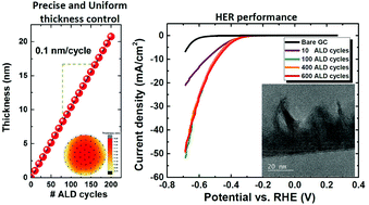
Low-temperature controllable synthesis of monolayer-to-multilayer thick MoS2 with tuneable morphology is demonstrated by using plasma enhanced atomic layer deposition (PEALD). The characteristic self-limiting ALD growth with a growth-per-cycle of 0.1 nm per cycle and digital thickness control down to a monolayer are observed with excellent wafer scale uniformity. The as-deposited films are found to be polycrystalline in nature showing the signature Raman and photoluminescence signals for the mono-to-few layered regime. Furthermore, a transformation in film morphology from in-plane to out-of-plane orientation of the 2-dimensional layers as a function of growth temperature is observed. An extensive study based on high-resolution transmission electron microscopy is presented to unravel the nucleation mechanism of MoS2 on SiO2/Si substrates at 450 °C. In addition, a model elucidating the film morphology transformation (at 450 °C) is hypothesized. Finally, the out-of-plane oriented films are demonstrated to outperform the in-plane oriented films in the hydrogen evolution reaction for water splitting applications.


 Please wait while we load your content...