
 Open Access Article
 This Open Access Article is licensed under a
 Creative Commons Attribution 3.0 Unported Licence
Electron microscopy of polyoxometalate ions on graphene by electrospray ion beam deposition†
N.
Vats
 *a,
S.
Rauschenbach
ab,
W.
Sigle
a,
S.
Sen
a,
S.
Abb
a,
A.
Portz
c,
M.
Dürr
c,
M.
Burghard
a,
P. A.
van Aken
a and
K.
Kern
ad
*a,
S.
Rauschenbach
ab,
W.
Sigle
a,
S.
Sen
a,
S.
Abb
a,
A.
Portz
c,
M.
Dürr
c,
M.
Burghard
a,
P. A.
van Aken
a and
K.
Kern
ad
aMax Planck Institute for Solid State Research, Heisenbergstrasse 1, D-70569 Stuttgart, Germany. E-mail: N.Vats@fkf.mpg.de
bDepartment of Chemistry, University of Oxford, OX2, Oxford, UK
cInstitut für Angewandte Physik, Justus-Liebig-Universität Giessen, Heinrich-Buff-Ring 16, 35392 Giessen, Germany
dInstitut de Physique, École Polytechnique Fédérale de Lausanne, CH-1015 Lausanne, Switzerland
First published on 22nd February 2018
Abstract
Aberration-corrected high-resolution transmission electron microscopy (AC-HRTEM) has enabled atomically resolved imaging of molecules adsorbed on low-dimensional materials like carbon nanotubes, graphene oxide and few-layer-graphene. However, conventional methods for depositing molecules onto such supports lack selectivity and specificity. Here, we describe the chemically selective preparation and deposition of molecules-like polyoxometalate (POM) anions [PW12O40]3− using electrospray ion-beam deposition (ES-IBD) along with high-resolution TEM imaging. This approach provides access to sub-monolayer coatings of intact molecules on freestanding graphene, which enables their atomically resolved ex situ characterization by low-voltage AC-HRTEM. The capability to tune the deposition parameters in either soft or reactive landing mode, combined with the well-defined high-vacuum deposition conditions, renders the ES-IBD based method advantageous over alternative methods such as drop-casting. Furthermore, it might be expanded towards depositing and imaging large and nonvolatile molecules with complex structures.
Introduction
The combination of high-resolution transmission electron microscopy (HRTEM) with modern aberration correctors offers sub-Ångstrom spatial resolution, which allows the imaging of individual atoms in bulk and nanoscale systems.1,2 HRTEM has been successfully employed to resolve atomic structures and crystallographic defects in a variety of material systems.3However, due to the radiation sensitivity of two-dimensional (2D) materials such as graphene, transition-metal-dichalcogenides (TMDs), hexagonal boron nitride (h-BN), or nanoparticles and molecules, the operation of TEM at lower acceleration voltages (i.e. 20–80 kV) is critical to minimize the knock-on damage.4,5 Recent developments in HRTEM instrumentation (cooling holders, low-dose imaging, stability and ultra-high vacuum) in tandem with advanced sample preparation techniques such as cryo-preparation methods6 and specimen encapsulation7–12 have not only attracted wide-spread attention, but also enabled scientists to further their research in single-molecule imaging down to the sub-molecular regime with minimal radiation damage. Most importantly, aberration-corrected TEM greatly advanced the structure determination via cryo-electron microscopy, where image averaging allows to reach atomic resolution also for complex 3D (bio-)molecular systems.13
However, high-precision HRTEM structural characterization of complex molecules on solid surfaces is limited by challenges in deposition techniques. This limits the ability to achieve high-chemical-purity molecular films and selective immobilization of atoms, molecules and complex aggregates on substrates. While atomic-scale characterization of structure and symmetry of individual molecules by HRTEM is in principle feasible, this critically depends on the preparation of suitable samples. The discovery of 2D materials such as graphene led to ultrathin electron-transparent substrates, on which the observation of individual atomic defects has been demonstrated.14–18 In addition, only a chemically pure, contamination- and destruction-free sample deposition of analyte molecules can enable us to correlate the observed structural features to the molecule under investigation. To this end, solution-based deposition techniques can be challenging as unwanted contaminations such as salts or organic residues are left behind and complicate the data analysis. By comparison, vacuum-based evaporation is inherently clean, but in many cases hindered by the lack of volatility of the molecule of interest.
As an alternative to vacuum-based evaporation, electrospray ionization (ESI)19–21 is a source of intact gas-phase molecular ions, which is widely used in vacuum-based analytical methods like mass spectrometry.20 Recently, with soft-landing electrospray ion beam deposition (ES-IBD),22–25 a preparative mass-spectrometry approach became available for the intact, chemically pure preparation of non-volatile macromolecules in vacuum. This method was successfully demonstrated for the preparation of individual molecular species imaged by scanning tunnelling microscopy.
Electrospray ionization serves to generate intact molecular gas phase ions from solution and gives access even to non-volatile molecules for vacuum deposition. The ion generation in ambient conditions is followed by a vacuum transfer, mass filtering with radio-frequency ion optics to obtain a pure beam, and finally ion deposition in high vacuum (10−6 mbar). The impact energy can be freely adjusted in this experiment by applying bias voltages to the sample holder, accelerating or decelerating the molecular ion before the impact. At sufficiently low impact energy, fragmentation can be avoided.26 On the other hand, molecule deposition at high impact energy can induce an interfacial reaction that leads to surface functionalization via covalent bonding.27,28 Independent of the detailed molecular anchoring mechanism, ES-IBD might further enable the growth of larger 2D molecular assemblies29 or even ultrathin films on substrates like graphene.
Here, we explore imaging of single molecules by AC-HRTEM by depositing them on freestanding graphene by ES-IBD in vacuum. This approach combines the advantages of freestanding graphene as a substrate with the highly pure, chemically selective deposition of mass-filtered molecular ion beams. Therefore, it allows high-resolution imaging30 while ensuring an unambiguous identification of the observed structures.
We use the molecule-like polyoxometalate (POM) anion [PW12O40]3− (phosphotungstate anion, PTA) which is an excellent model system for this study. POM anions like PTA have a cluster-like inorganic structure, which makes them less prone to radiation damage in comparison to organic molecules. Additionally, the W atoms will provide an excellent contrast in TEM. In previous TEM studies, POMs have been atomically resolved on 2D electron-transparent substrates such as GO and covalently-functionalized few-layer graphene (FLG).15–17,31 In contrast, TEM analysis of POMs on single-layer graphene (SLG) substrates has not been investigated yet. Beside their unique structural aspects, POMs are of interest for various applications, including surface catalysis and nanoscale magnetism.32–34 After PTA deposition, the samples are transferred ex situ to the electron microscope and they are characterized using low-voltage AC-HRTEM.
Materials and methods
The PTA used in our experiment was purchased from Fluka chemicals (99.95% purity). The PTA consists of a central PO4 tetrahedral group surrounded by 12 WO6 octahedral groups as a shell, which are linked together by shared oxygen atoms, as shown in Fig. 1a. It comprises 40 oxygen atoms, 12 tungsten atoms, and one phosphorus atom, which add up to a molecular mass of 2877.1 g mol−1.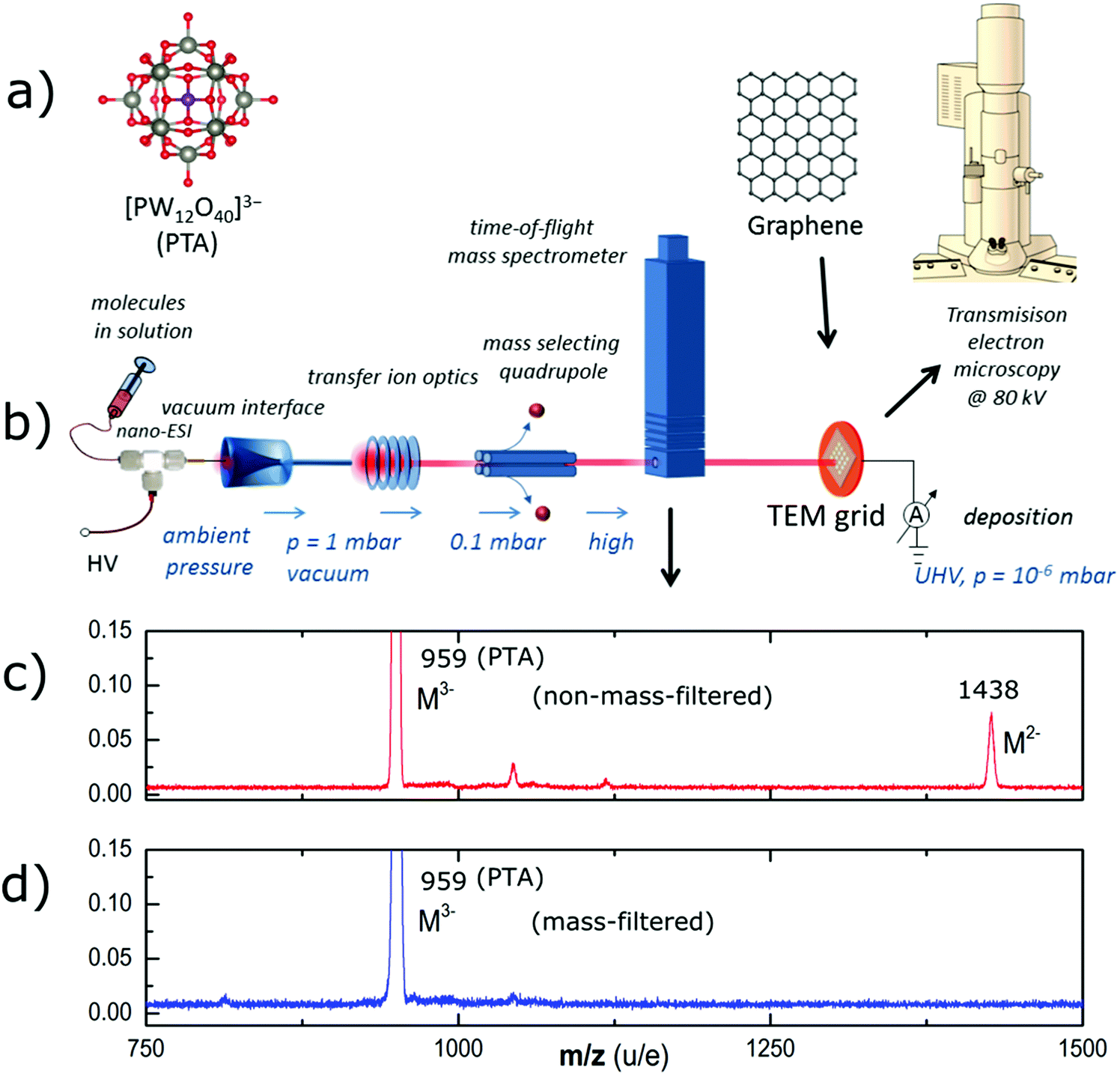 | ||
| Fig. 1 (a) Ball-and-stick model of the PTA molecule (b) schematic of the molecule deposition process using ES-IBD. Molecules are ionized by ESI from solution, transferred into vacuum where a beam is collimated, mass-filtered and mass analysed before deposition. The final step is the ex situ transfer to the electron microscope. (c) Mass spectrum of PTA before and (d) after mass selection, as used for deposition. | ||
Graphene transfer on TEM grid
PMMA-free graphene suspended on a TEM grid was fabricated similar to the method described by Longchamp et al.30 Commercially available CVD-grown graphene on copper foil (Graphenea S.A.) was used throughout our experiments. As the first step, a 150 nm thick PMMA film was spin-coated onto the graphene on Cu. The copper film was then etched by floating the PMMA-SLG-Cu assembly in an etching solution (8 g of ammonium persulfate in 100 mL of deionized water). After Cu etching, the PMMA–graphene stack was transferred to a deionized water bath for removing the APS solution residue. Subsequently, the stack was transferred onto the platinum-coated (thickness ∼15 nm) perforated silicon nitride TEM grid by fishing. In order to remove the PMMA, the TEM grid was annealed in ambient air at 300 °C for 30 minutes, whereupon the thin platinum layer catalyses the oxidation of the PMMA (Fig. 2a).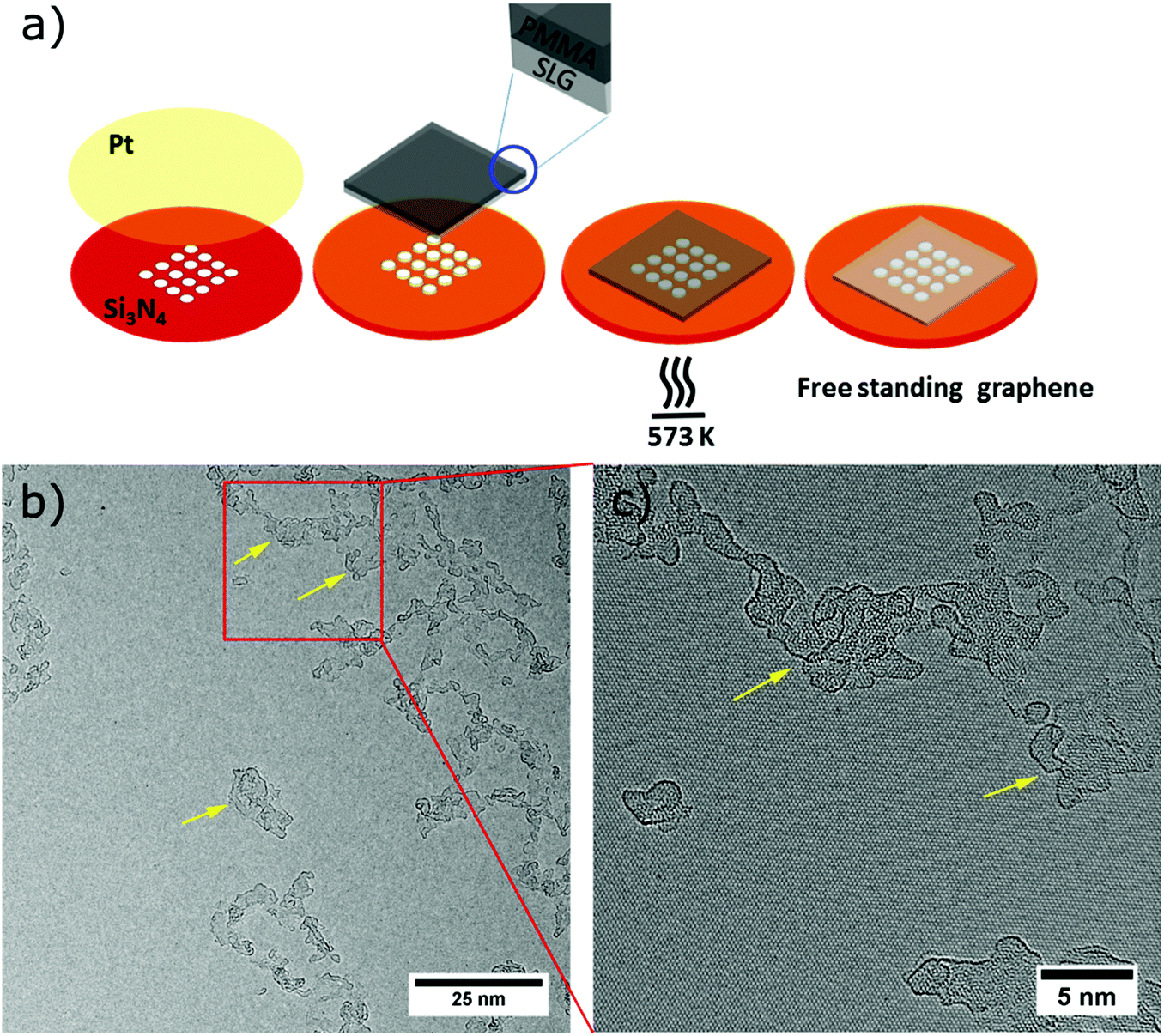 | ||
| Fig. 2 Graphene sample preparation before deposition. (a) Scheme of preparing clean SLG using platinum metal catalysis. Platinum (Pt) is sputtered onto a perforated silicon nitride (Si3N4) TEM grid, then the SLG supported by PMMA is transferred onto Pt coated Si3N4 TEM grid. In the next step, the PMMA is removed by annealing the grid at 573 K for 30 minutes which provides clean and free standing SLG on a holey silicon nitride TEM grid. (b) Low-magnification TEM micrograph of free standing graphene showing large clean areas alongside amorphous hydrocarbon impurities (yellow arrows). (c) Magnified AC-HRTEM image showing details of the hydrocarbon impurities and clean graphene. | ||
Electrospray ion-beam deposition (ES-IBD)
The electrospray ion-beam deposition setup (Fig. 1b) is used to generate intact negative gas phase ions of PTA and deposit them on the graphene substrate in vacuum.23,25 The analyte solution (∼10−4 mol l−1 PTA in acetonitrile) is pumped through an emitter capillary held at a high electric potential difference of 2–3 kV with respect to the vacuum transfer capillary. A fine mist of charged droplets containing the analyte molecule is emitted. The ions are generated under ambient conditions through iterative Coulombic fission while the solvent evaporates. They pass through four differential pumping stages to the deposition target held at 10−6 mbar. On their way, radio frequency (rf)-ion optics collimates the beam, with an ion funnel in the first and an rf-only quadrupole in the second stage. A further rf-quadrupole is used as a mass filter to generate a chemically pure beam of the desired ion, which is confirmed by an integrated TOF mass spectrometer before the beam is used for deposition. Fig. 1c shows the mass spectrum of the generated ion beam before and Fig. 1d after mass–charge-ratio (m/z) filtering the POM3− ion at m/z 959 (throughout the paper the term mass-to-charge ratio m/z represents atomic mass number per number of elementary charges). The salient feature of ES-IBD is that the collision energy can be controlled and thereby the interaction of the molecule with the surface.26 Most importantly, molecules can be soft-landed destruction-free onto the surface or collided at high energies to deliberately cause fragmentation or surface defects. Further, online current monitoring allows for precise knowledge of the deposited charge and thus for the control of the deposition coverage.AC-HRTEM imaging and image simulation
AC-HRTEM was performed using a JEOL ARM 200F TEM equipped with a cold field-emission gun and a post-specimen spherical aberration corrector (Cs) operated at an acceleration voltage of 80 kV. The spherical aberration was tuned to approximately 1 μm, and the imaging was done at under-focus conditions, leading to atoms appearing dark. HRTEM image simulations were conducted using the multi-slice QSTEM software package.35 For image simulations, the spherical aberration Cs was set to 1 μm, the acceleration voltage to 80 kV and the defocus was set to −2.5 nm, corresponding to the Scherzer defocus. From the obtained images, several quantities were extracted.Data analysis
To estimate the area density of individual tungsten atoms, i.e., atoms which are neither a part of a PTA nor a larger agglomeration, we used four HRTEM images of four different regions with a field of view of 31 × 31 nm2 and averaged the number of atoms in each HRTEM image. This procedure was applied for samples on which PTAs were landed with 15 eV, 150 eV, and 300 eV landing energies, respectively. Similarly, the area coverage by landed PTAs and their agglomerates was calculated by taking the ratio of area occupied by one PTA and the area of the entire field of view (31 × 31 nm2). The median value was calculated of the available data in the graph representing the coverage area, in order to provide a better measure of the central tendency. As the number of data points is less (four in this particular case), calculating the median offers a better statistical understanding of the data-set available.DINeC
Desorption/Ionization Induced by Neutral Clusters (DINeC)36,37 was used as a soft desorption/ionization method for analysing the adsorbed molecules. In short, neutral SO2 clusters (103 to 104 molecules in size) which are seeded in a helium beam hit the surface and softly desorb and ionize some of the adsorbates.36 The latter are then transferred into a commercial ion trap mass spectrometer (Bruker amaZon speed)37 for mass analysis.Results and discussion
Initial TEM characterisation
AC-HRTEM investigation of the cleaned SLG samples (Fig. 2b and c) revealed the presence of large areas of bare single-layer graphene along with areas of amorphous hydrocarbon impurities (marked by yellow arrows). These amorphous impurities undergo graphitization under an electron beam38 and are of similar transparency like the graphene. Based on our observation, these regions are only one or two atomic layers thick. The presence of these polyaromates or hydrocarbons39–41 on the surface of the SLG reveals that the catalytic cleaning by the platinum did not leave the graphene completely clean. In contrast to the data presented by Longchamp et al.,30 who developed the method used here, in our experiments the graphene is not entering the vacuum while being still hot, but is exposed to the contamination present in ambient air during the transfer.41,42Nevertheless, as shown in Fig. 2b and c the samples comprise large areas of clean graphene alongside electron transparent ultrathin amorphous areas, both of which allow for TEM investigation of deposited species.
Ion beams and deposition
The mass spectrum (Fig. 1d) shows the PTA ion beam without mass filtering. Intense peaks at (m/z) 959 and 1438 can be identified as the triple and double negatively charged molecular ion, respectively. Additionally, several other peaks indicate the presence of other unidentified ions being contamination or fragments. After mass-selection we only observe the peak of the triple-charged PTA anion at (m/z) 959. Other charge states or contamination peaks are absent or suppressed to approximately 1% of the base-peak intensity. Considering the peak area as a rough approximation for the intensity, the purity of the beam is estimated to be well above 99%.Following the mass selection, the kinetic energy of the beam is measured and the collision energy with the surface is set by applying a sample voltage (Vsample) according to the desired collision energy per charge Ecoll/z = Ekin/z − Vsample. For the present experiments, deposition energies of 15 eV, 150 eV, 300 and 750 eV per molecule were chosen, corresponding to energy per charge values of 5 eV per charge, 50 eV per charge, 100 eV per charge, and 250 eV per charge, respectively.
Moreover, the surface coverage (θ) can be selected via the online current monitoring performed during deposition. It is related to the deposited charge Q and can be calculated for the given substrate area Asample using the relation θ = (Q/ze)(Amolecule/Asample), where z is the charge state of the molecular ion, e is the elementary charge, and Amolecule the cross section area of one molecule. The samples shown here were coated with 50 pAh, 500 pAh, and 2000 pAh (with 1 pAh = 3.6 × 10⁻⁹ Coulomb). For a given charge the surface coverage θ can be calculated for a known deposition area A (approximately 10 mm2), resulting in 30 molecules per 31 × 31 nm2 area (the size of the micrographs in Fig. 3 and 6) for three charges per ion for 50 pAh, 300 molecules for 500 pAh, and 1200 molecules for 2000 pAh. The latter value roughly corresponds to complete monolayer coverage.
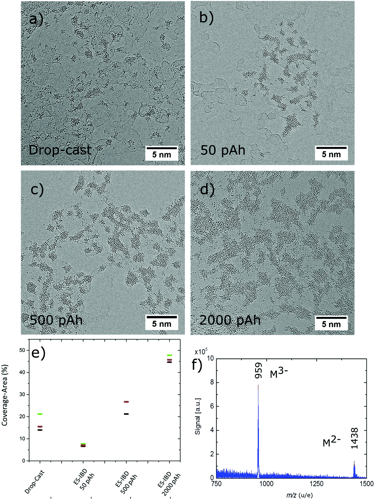 | ||
| Fig. 3 AC-HRTEM micrograph showing the morphology of PTA molecular adsorbates on SLG after deposition via (a) drop-casting, (b–d) ES-IBD at different coverage (50, 500 and 2000 pAh deposited charge). (e) Maximum, minimum and median values (represented by green, black and red horizontal bars) shows area of coverage obtained during ES-IBD and drop-casting method analysed for four samples. (f) Negative ion mass spectrum of molecules desorbed by means of DINeC after soft landing on a gold surface. The main peaks at m/z = 959 and 1438 correspond to the intact PTA molecule. | ||
AC-HRTEM imaging of PTA
The AC-HRTEM images of PTA molecules on SLG in Fig. 3a–d compare the results of two different molecular deposition methods, namely solution drop-cast (Fig. 3a) and ES-IBD soft landing at 5 eV per charge (Fig. 3b–d). Both deposition methods lead to aggregates of PTA, which can be easily recognized due to the strong contrast of the W atoms versus the carbon-based substrate of graphene and amorphous hydrocarbon.Another common feature observed in the four images is that the PTAs almost exclusively stick to the amorphous carbon layers rather than to the pristine SLG surface. In contrast, the morphologies resulting from the two preparation approaches are different. Specifically, solvent deposition leads to atomic clusters that vary significantly in size, ranging from single atoms to agglomerates extending over several nanometres (Fig. 3a). By comparison, molecular ion beam deposition (Fig. 3b–d) results in groups of ramified islands located on the amorphous hydrocarbon impurities. As the deposited charge is increased from 50 pAh to 2000 pAh, the number and size of these groups increases from ∼1.7 nm2 at 50 pAh to ∼9 nm2 (see Fig. 3e), while their general morphology remains unchanged (see also ESI Table S6(a–d)†).
The difference in morphology between solution and ion beam deposition reflects the different capabilities of these two methods with respect to control of coverage, cleanliness, and homogeneity. While the solution deposition is governed by a drying process, which is not well-defined and thus is prone to contamination, ES-IBD offers a chemically well-defined, homogeneous beam, which impinges on the surface evenly with controllable coverage. Consequently, ion beam deposition is capable to produce a uniform coating in contrast to solution deposition, which is inherently inhomogeneous. The control over the coverage is illustrated in Fig. 3e, showing the area coverage analysed for four different values of totally deposited charge. The coverage for ES-IBD samples gradually is seen to increase as the charge deposited on the sample is increased from 50 pAh to 2000 pAh. The observed coverage area is 6% for the 50 pAh, 25% for the 500 pAh, and 46% for 2000 pAh deposition. The slower rise of coverage vs. deposited charge can be attributed to closer packing and/or an enhanced three-dimensional aspect of the formed structures when they grow larger. Similarly, a density gradient at the edge of the sample becomes more pronounced and causes an increased spread in the observed coverage with deposited charge. For comparison, the largest spread was observed for the drop-cast samples, ranging from 14% to 20% area coverage, all produced with one solution and for the same deposition conditions.
While a similar homogeneity in the coverage might be achievable for the solution deposition, clearly these samples are inferior to the ES-IBD samples in cleanliness and homogeneity of the overall morphology. In Fig. 3a, the dimensions of the observed adsorbates range from single atom size (0.2 nm) to large agglomerations (5 nm diam.) for the solution deposition. For ion-beam deposition, the agglomerate dimension starts with the size of the intact molecule, rising from 0.8 nm to 2 nm at lower coverage (50 pAh), to 1 nm to 2.5 nm (500 pAh), and finally to the range of 1.5 nm to 10 nm (2000 pAh) (see also ESI S6(a–d)†).
Since the intactness of the molecules cannot be directly inferred from the shape of the adsorbate, we verified the intact deposition of PTA through mass spectrometry measurements with the aid of the soft desorption/ionization method DINeC36,37 (see Materials and methods). For this purpose, we deposited 250 pAh of PTA on gold and transferred the sample ex situ to the DINeC-MS instrument. The mass spectrum in Fig. 3f closely resembles a clean ESI mass spectrum of PTA in the relevant m/z-range (compare to Fig. 1d). In particular, one observes intact triply and doubly charged PTA, with no sizeable background for m/z > 500. Note that the background intensity recorded in the DINeC mass spectrum at low m/z is likely due to contamination from the ex situ handling of the sample (see ESI Fig. S2†).
The PTA ensembles on the graphene membrane resulting from ES-IBD have a distinct, characteristic shape and are grouped closely together leaving large areas of substrate uncoated. Instead of the expected formation of compact patches for homogeneous, non-specific van der Waals interacting molecules of isotropic shape such as PTA, we observe elongated, ramified islands grouped closely together (see Fig. 3b–d and 6). The TEM images clearly show a striking resemblance of the PTA island morphology and of amorphous regions on the graphene. The agglomerates created by drop-cast deposition, in contrast, are randomly distributed and of random shape. In particular, the assembly lacks the characteristic grouping of molecular aggregates observable for ion beam deposition of PTA.
While the not well-defined nature of the solution deposition process makes it difficult to explain the resulting PTA distribution on the SLG, the observed morphology after ES-IBD can be qualitatively understood by considering diffusion and aggregation of the molecules on a surface. Upon deposition, the PTAs randomly attach over the entire surface. It is reasonable to assume that while the binding strength can be significant, the migration barriers are low, especially on clean graphene. On this basis, the PTAs would be able to migrate until they become immobilized, which happens preferably on the amorphous areas. In contrast to the SLG, the amorphous regions are not flat, but contain numerous defects that will act as pinning sites for the diffusing PTAs. These pinning sites are most likely inhomogeneities like step edges, heteroatoms, functional groups, vacancies, or other chemical defects, which are energetically favourable over pure sp2 graphene for such interactions.43,44 In addition, the charge of the deposited species could be retained,45 which might further enhance the pinning to such sites.
The inert surface of clean graphene does not provide suitable pinning sites for immobilization of the PTAs. Therefore, it is highly probable that the PTAs are mobile on the perfect crystalline surface of graphene and get immobilized at the edge of the hydrocarbon impurities lying on graphene. The fact that a large part of the amorphous carbon regions is completely unoccupied by the PTA can be understood by considering that the deposition is done only on one side, while the contamination most likely exists on both sides of the graphene.
Imaging single PTAs
Occasionally, small structures resembling one individual PTA are found outside of the agglomerations, one is highlighted by the red square in Fig. 4a, and shown magnified in Fig. 4b. The corresponding structural model is depicted in Fig. 4h with a simulated AC-HRTEM image shown in Fig. 4e. The PTA orientation was determined by comparing the image simulation based on with a table of possible orientations, calculated for the gas phase structure (ESI Fig. S1†).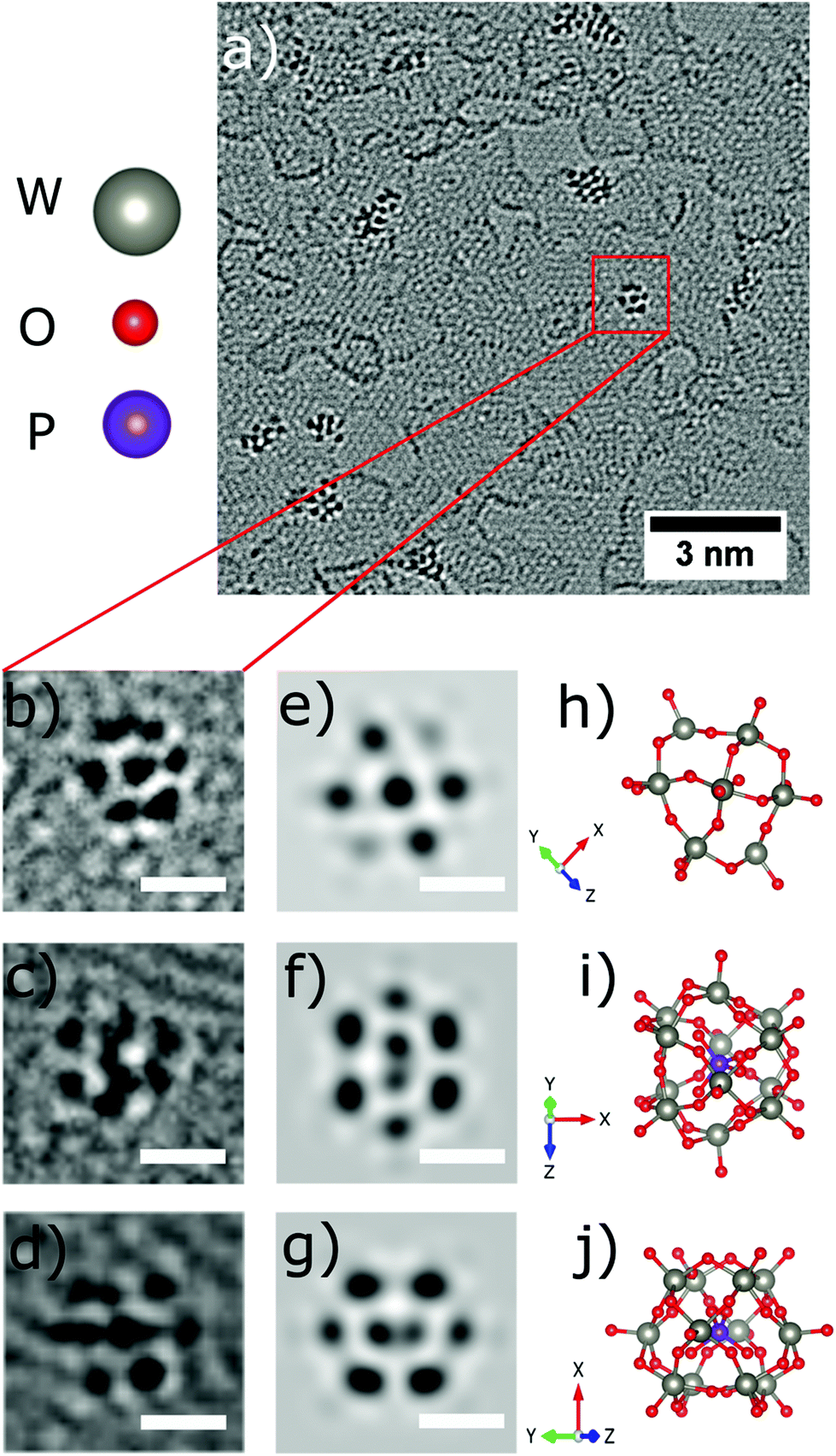 | ||
| Fig. 4 Observation of individual molecules on the graphene substrate (a). (b–d) AC-HRTEM images of individual PTA at different rotation angles (e–g) image simulation at 80 kV, spherical aberration Cs = 1 μm and defocus = −2.5 nm of the corresponding structural models. (h–j) Ball and stick structural model of PTA [PW12O40]3− anion molecule at different rotation angles. Tungsten (W) atoms grey, oxygen (O) red and phosphorus (P) atoms violet. All scale bars correspond to 0.5 nm. | ||
Four more examples are shown in Fig. 4c, d, 5b and e and are compared to model structures and simulated images in Fig. 4f, g, 5c and f, respectively. These individual objects are stable under the electron beam for a long time (more than 250s). Nevertheless, the irradiation enhanced the mobility of the PTAs, so that they started to laterally diffuse or rotate. (ESI Fig. S3† for a time series).
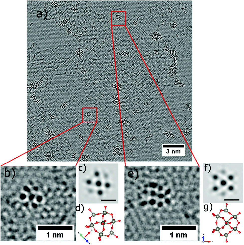 | ||
| Fig. 5 Observation of individual molecules on the graphene substrate (a). (b and e) AC-HRTEM images of individual PTA at different rotation angles (c and f) image simulation at 80 kV, spherical aberration Cs = 1 μm and defocus = −2.5 nm of the corresponding structural models. (d and g) Ball and stick structural model of PTA [PW12O40]3− anion molecule at different rotation angles. Tungsten (W) atoms grey, oxygen (O) red and phosphorus (P) atoms violet. Scale bars shown in (c and f) correspond to 0.5 nm. | ||
The Keggin-type [PW12O40]3− anion46 has two symmetry axes, specifically one C3 and one S4 axis. The phosphorus atom (violet colour) is located in the centre of the cage (see the structural models in Fig. 1c and 4i, j). For more examples of single PTA molecules we refer to Fig. S4 in the ESI.† However, the high-contrast feature in the AC-HRTEM micrograph of the PTA is attributed to the strong scattering from heavy tungsten atoms (Z = 74). It is highly unlikely that one observes the contrast from the single phosphorus atom (Z = 15) located in the centre, as it has much smaller Z in comparison to W. The image simulations (Fig. 4e–g) suggest that completely superimposed W atoms show sharper contrast than only partially overlapping W atoms.
Moreover, blurry contrasts in simulated images arise from oxygen atoms which are located at the periphery of a tungsten atom. Given the many possible orientations and further complications by close attachment of neighbouring molecules in the agglomerates, it becomes clear that the individual PTAs cannot be recognized in agglomerates but only if immobilized individually.
While the overall occurrence of the single molecule is rare, an unambiguous identification is possible due the chemically defined deposition from molecular ion beams. In contrast, while assemblies of 6 or 7 protrusions are also found for solution deposition, we cannot claim that these are single molecules due to the presence of many ill-shaped structures.
Influence of landing energy
It is well documented that the collision of the ions with the substrate surface may induce structural distortion of the ion and can cause surface modifications depending on the type of collision, i.e. elastic or inelastic.47 Therefore, by controlling the kinetic energy of the incoming ion, the nature of the collision between ion and surface can be tuned between soft or reactive (dissociative) landing. This can be exploited for chemical modification of the surface in a controlled environment. In fact, low energies are employed for soft-landing large biomolecules,23 proteins,22 and organometallic clusters,48 so as to achieve destruction-free deposition (physisorption) on surfaces, whereas at high energies reactive landing is used in order to anchor molecules at the surface by formation of covalent bonds.28In the present experiments, we employed four different landing energies for the PTA, specifically 15 eV, 150 eV, 300 eV, and 750 eV per anion, with the prime intention to land intact PTAs on the SLG and observe the transition from soft to reactive landing. It is worth to mention that reactive landing could be used on purpose to generate defects that can act as pinning sites for molecular binding on graphene. Finally, for freestanding graphene as a 2D substrate, the generation of holes in the material by the impinging ions might occur. The AC-HRTEM images in Fig. 6a–d display PTA ensembles resulting from ES-IBD at 15 eV, 150 eV, 300 eV, and 750 eV per ion, respectively. Interestingly, no holes have been produced by the impact of the energetic PTA ions. In all cases, tungsten-containing adsorbates are formed on the surface. For the soft landing energy (Fig. 6a) the agglomerations have the morphology already described: intact PTAs are arranged in groups of agglomerations immobilized on the amorphous part of the substrate. The morphology changes with increasing landing energy. For 150 eV, the agglomerations look similar, although the clusters are distributed more evenly (Fig. 6b). In contrast, at 300 and 750 eV we did not observe the assembly of molecular aggregates as we did at lower landing energies. Instead, the AC-HRTEM images rather resemble the drop cast results (Fig. 3a), with a random distribution of large undefined W-containing clusters along with individual W atoms (Fig. 6c and d).
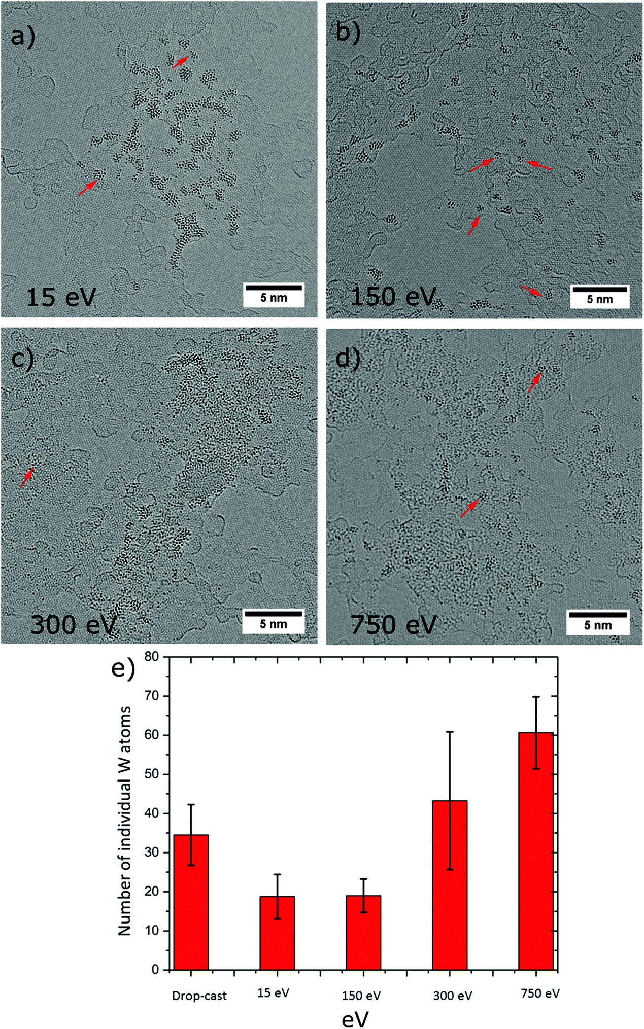 | ||
| Fig. 6 AC-HRTEM micrographs of the adsorbates after deposition of 50 pAh PTA anions at landing energies of (a) 15 eV, (b) 150 eV, (c) 300 eV and (d) 750 eV per molecule. Individual PTA molecules (marked by red arrows) molecular aggregates and molecular fragments down to the individual tungsten atom (individual black dots) are observed. (e) Number of individual W atoms observed on graphene (per 31 × 31 nm2) indicates increased fragmentation for deposition above 300 eV and for drop casting. | ||
An analysis of the number of single-atom impurities underpins the rising occurrence of damaged molecules above 150 eV. For energies below this value soft landing occurs, whereas a deposition at higher energies (300 eV and 750 eV) yields numerous individual W atoms and a comparatively smaller size of the agglomerates (see ESI Table S7(a–d)†). This observation is in agreement with other experiments of surface-induced dissociation by molecular ion collision observed for organic molecules and clusters.28,49 Furthermore, it is intriguing that even at the highest energy, when the PTA molecule is destroyed, the graphene appears unaffected. This testifies the high mechanical stability of this 2D material. While the kinetic energy amounts to several C–C bond energies, this behaviour can be understood when considering how the energy is dissipated. Comparing the time scales of molecular vibrations (femto seconds) with the duration of the collision event (1 ps at 15 eV to 0.15 ps for 750 eV), the collision is a relatively slow process. This allows dissipating the deposited energy into available vibrational degrees of freedom. In this manner, the graphene is able to distribute energy swiftly and is not destroyed, which is not possible in the case of the PTA at high deposition energy, due to its lower dimensionality and generally lower number of available vibrational modes.26
Conclusion
In summary, we successfully demonstrated the chemically selective deposition and subsequent AC-HRTEM imaging of PTAs on freestanding graphene with reliable chemical and coverage control. The cluster ions physiosorb onto the graphene and remain mobile until they get pinned at hydrocarbon impurities present on the graphene surface. Importantly, the PTAs remained intact under the e-beam for prolonged irradiation during AC-HRTEM observation.In addition, we showed that the PTA deposition can be adjusted from soft to destructive landing. At low and intermediate landing energies (15 and 150 eV per ion), densely arranged aggregates consisting of intact PTAs are formed. By contrast, at very high landing energies (above 300 eV per ion) PTA fragmentation occurs. Interestingly, under this condition graphene preserved its structural integrity, while the PTAs suffered from dissociation upon colliding with the graphene surface.
Thus far, PTA immobilization could be observed only at hydrocarbon impurities present on graphene. Accordingly, protocols for the controllable immobilization of the deposited species still need to be developed. The creation of pinning sites by energetic impact50 would be difficult, as the stability of graphene exceeds that of any molecule to be deposited. One possibility could be the creation of single or multiple vacancies by small ion impact, or through solution-based chemical functionalization of graphene. Furthermore, it became evident that TEM imaging is strongly facilitated by deposition of the species under clean and well-defined conditions. In order to avoid the introduction of contaminations upon substrate transfer through the ambient, it would be best to perform both, the creation of anchoring sites (defects) in graphene and the deposition process in an in situ environment.
Overall, our findings highlight the usefulness of a chemically selective deposition methodology for AC-HRTEM imaging, and provide a suitable basis for further investigations of the interaction of molecules with free-standing SLG. Soft ionization, soft deposition in vacuum, and the ability of mass filtering to select only a desired molecular ion species to be landed intact on a clean and well-defined surface, distinguishes the ES-IBD approach from other molecular deposition techniques. On this basis, it might prove essential for TEM investigation of large molecules with complex features, in particular since ES-IBD offers access to the vast majority of non-volatile macromolecules.25,51–53
Conflicts of interest
There are no conflicts to declare.Acknowledgements
We would like to thank Yvonne Stuhlhofer and Stephan Schmid (MPI-FKF) for platinum deposition on TEM grids and Yi Wang (MPI-FKF) for helpful discussion on HRTEM image simulation. Open Access funding provided by the Max Planck Society.Notes and references
- M. Haider, G. Braunshausen and E. Schwan, Optik, 1995, 99, 167–179 Search PubMed.
- P. Batson, N. Dellby and O. Krivanek, Nature, 2002, 418, 617–620 CrossRef CAS PubMed.
- D. B. Williams and C. B. Carter, in Transmission electron microscopy, Springer, 1996, pp. 3–17 Search PubMed.
- U. Kaiser, J. Biskupek, J. C. Meyer, J. Leschner, L. Lechner, H. Rose, M. Stöger-Pollach, A. N. Khlobystov, P. Hartel, H. Müller, M. Haider, S. Eyhusen and G. Benner, Ultramicroscopy, 2011, 111, 1239–1246 CrossRef CAS PubMed.
- K. Suenaga, Y. Iizumi and T. Okazaki, Eur. Phys. J.: Appl. Phys., 2011, 54, 33508 CrossRef.
- R. Henderson, J. M. Baldwin, T. A. Ceska, F. Zemlin, E. Beckmann and K. H. Downing, J. Mol. Biol., 1990, 213, 899–929 CrossRef CAS PubMed.
- K. Hirahara, K. Suenaga, S. Bandow, H. Kato, T. Okazaki, H. Shinohara and S. Iijima, Phys. Rev. Lett., 2000, 85, 5384–5387 CrossRef CAS PubMed.
- X. Fan, E. Dickey, P. Eklund, K. Williams, L. Grigorian, R. Buczko, S. Pantelides and S. Pennycook, Phys. Rev. Lett., 2000, 84, 4621 CrossRef CAS PubMed.
- J. Sloan, G. Matthewman, C. Dyer-Smith, A. Y. Sung, Z. Liu, K. Suenaga, A. I. Kirkland and E. Flahaut, ACS Nano, 2008, 2, 966–976 CrossRef CAS PubMed.
- J. M. Yuk, J. Park, P. Ercius, K. Kim, D. J. Hellebusch, M. F. Crommie, J. Y. Lee, A. Zettl and A. P. Alivisatos, Science, 2012, 336, 61–64 CrossRef CAS PubMed.
- Q. Chen, J. M. Smith, J. Park, K. Kim, D. Ho, H. I. Rasool, A. Zettl and A. P. Alivisatos, Nano Lett., 2013, 13, 4556–4561 CrossRef CAS PubMed.
- C. Wang, Q. Qiao, T. Shokuhfar and R. F. Klie, Adv. Mater., 2014, 26, 3410–3414 CrossRef CAS PubMed.
- R. Henderson, Arch. Biochem. Biophys., 2015, 581, 19–24 CrossRef CAS PubMed.
- A. Markevich, S. Kurasch, O. Lehtinen, O. Reimer, X. Feng, K. Mullen, A. Turchanin, A. N. Khlobystov, U. Kaiser and E. Besley, Nanoscale, 2016, 8, 2711–2719 RSC.
- X. Ke, S. Turner, M. Quintana, C. Hadad, A. Montellano-López, M. Carraro, A. Sartorel, M. Bonchio, M. Prato, C. Bittencourt and G. Van Tendeloo, Small, 2013, 9, 3922–3927 CrossRef CAS PubMed.
- J. Sloan, Z. Liu, K. Suenaga, N. R. Wilson, P. A. Pandey, L. M. Perkins, J. P. Rourke and I. J. Shannon, Nano Lett., 2010, 10, 4600–4606 CrossRef CAS PubMed.
- C. Bosch-Navarro, L. M. Perkins, R. J. Kashtiban, J. P. Rourke, I. J. Shannon and J. Sloan, ACS Nano, 2016, 10, 796–802 CrossRef CAS PubMed.
- R. R. Nair, P. Blake, J. R. Blake, R. Zan, S. Anissimova, U. Bangert, A. P. Golovanov, S. V. Morozov, A. K. Geim, K. S. Novoselov and T. Latychevskaia, Appl. Phys. Lett., 2010, 97, 153102 CrossRef.
- L. Konermann, E. Ahadi, A. D. Rodriguez and S. Vahidi, Anal. Chem., 2013, 85, 2–9 CrossRef CAS PubMed.
- J. Fenn, M. Mann, C. Meng, S. Wong and C. Whitehouse, Science, 1989, 246, 64–71 CAS.
- M. Yamashita and J. B. Fenn, J. Phys. Chem., 1984, 88, 4451–4459 CrossRef CAS.
- Z. Ouyang, Z. Takáts, T. A. Blake, B. Gologan, A. J. Guymon, J. M. Wiseman, J. C. Oliver, V. J. Davisson and R. G. Cooks, Science, 2003, 301, 1351–1354 CrossRef CAS PubMed.
- S. Rauschenbach, F. L. Stadler, E. Lunedei, N. Malinowski, S. Koltsov, G. Costantini and K. Kern, Small, 2006, 2, 540–547 CrossRef CAS PubMed.
- J. Laskin, P. Wang and O. Hadjar, Phys. Chem. Chem. Phys., 2008, 10, 1079–1090 RSC.
- S. Rauschenbach, M. Ternes, L. Harnau and K. Kern, Annu. Rev. Anal. Chem., 2016, 9, 473–498 CrossRef CAS PubMed.
- S. Rauschenbach, R. Vogelgesang, N. Malinowski, J. W. Gerlach, M. Benyoucef, G. Costantini, Z. Deng, N. Thontasen and K. Kern, ACS Nano, 2009, 3, 2901–2910 CrossRef CAS PubMed.
- C. Evans, N. Wade, F. Pepi, G. Strossman, T. Schuerlein and R. G. Cooks, Anal. Chem., 2002, 74, 317–323 CrossRef CAS PubMed.
- G. Dubey, R. Urcuyo, S. Abb, G. Rinke, M. Burghard, S. Rauschenbach and K. Kern, J. Am. Chem. Soc., 2014, 136, 13482–13485 CrossRef CAS PubMed.
- S. Abb, L. Harnau, R. Gutzler, S. Rauschenbach and K. Kern, Nat. Commun., 2016, 7, 10335 CrossRef CAS PubMed.
- J.-N. Longchamp, C. Escher and H.-W. Fink, J. Vac. Sci. Technol., B: Nanotechnol. Microelectron.: Mater., Process., Meas., Phenom., 2013, 31, 020605 Search PubMed.
- V. Prabhakaran, B. L. Mehdi, J. J. Ditto, M. H. Engelhard, B. Wang, K. D. D. Gunaratne, D. C. Johnson, N. D. Browning, G. E. Johnson and J. Laskin, Nat. Commun., 2016, 7, 11399 CrossRef CAS PubMed.
- M. T. Pope and A. Müller, Angew. Chem., Int. Ed. Engl., 1991, 30, 34–48 CrossRef.
- D.-L. Long, E. Burkholder and L. Cronin, Chem. Soc. Rev., 2007, 36, 105–121 RSC.
- D.-L. Long, R. Tsunashima and L. Cronin, Angew. Chem., Int. Ed., 2010, 49, 1736–1758 CrossRef CAS PubMed.
- C. T. Koch, Determination of core structure periodicity and point defect density along dislocations, 2002 Search PubMed.
- C. R. Gebhardt, A. Tomsic, H. Schröder, M. Dürr and K. L. Kompa, Angew. Chem., Int. Ed., 2009, 48, 4162–4165 CrossRef CAS PubMed.
- M. Baur, C. R. Gebhardt and M. Dürr, Rapid Commun. Mass Spectrom., 2014, 28, 290–296 CrossRef CAS PubMed.
- F. Börrnert, S. M. Avdoshenko, A. Bachmatiuk, I. Ibrahim, B. Büchner, G. Cuniberti and M. H. Rümmeli, Adv. Mater., 2012, 24, 5630–5635 CrossRef PubMed.
- R. Zan, U. Bangert, Q. Ramasse and K. S. Novoselov, Nano Lett., 2011, 11, 1087–1092 CrossRef CAS PubMed.
- R. Zan, U. Bangert, Q. Ramasse and K. S. Novoselov, J. Phys. Chem. Lett., 2012, 3, 953–958 CrossRef CAS PubMed.
- G. Algara-Siller, O. Lehtinen, A. Turchanin and U. Kaiser, Appl. Phys. Lett., 2014, 104, 153115 CrossRef.
- S. Davidson, Measurement, 2007, 40, 762–768 CrossRef.
- O. Cretu, A. V. Krasheninnikov, J. A. Rodríguez-Manzo, L. Sun, R. M. Nieminen and F. Banhart, Phys. Rev. Lett., 2010, 105, 196102 CrossRef PubMed.
- F. Banhart, J. Kotakoski and A. V. Krasheninnikov, ACS Nano, 2011, 5, 26–41 CrossRef CAS PubMed.
- K. D. D. Gunaratne, V. Prabhakaran, A. Andersen, G. E. Johnson and J. Laskin, Phys. Chem. Chem. Phys., 2016, 18, 9021–9028 RSC.
- J. F. Keggin, Proc. R. Soc. London, Ser. A, 1934, 144, 75–100 CrossRef CAS.
- G. E. Johnson, D. Gunaratne and J. Laskin, Mass Spectrom. Rev., 2016, 35, 439–479 CrossRef CAS PubMed.
- C. Copéret, M. Chabanas, R. Petroff Saint-Arroman and J.-M. Basset, Angew. Chem., Int. Ed., 2003, 42, 156–181 CrossRef PubMed.
- P. Wang, O. Hadjar, P. L. Gassman and J. Laskin, Phys. Chem. Chem. Phys., 2008, 10, 1512–1522 RSC.
- S. Habenicht, W. Bolse, H. Feldermann, U. Geyer, H. Hofsäss, K. Lieb and F. Roccaforte, Europhys. Lett., 2000, 50, 209 CrossRef CAS.
- J.-N. Longchamp, S. Rauschenbach, S. Abb, C. Escher, T. Latychevskaia, K. Kern and H.-W. Fink, Proc. Natl. Acad. Sci. U. S. A., 2017, 114, 1474–1479 CrossRef CAS PubMed.
- G. Rinke, S. Rauschenbach, L. Harnau, A. Albarghash, M. Pauly and K. Kern, Nano Lett., 2014, 14, 5609–5615 CrossRef CAS PubMed.
- G. Rinke, S. Rauschenbach, S. Schrettl, T. N. Hoheisel, J. Blohm, R. Gutzler, F. Rosei, H. Frauenrath and K. Kern, Int. J. Mass Spectrom., 2015, 377, 228–234 CrossRef CAS.
Footnote |
| † Electronic supplementary information (ESI) available: HRTEM image simulation tableau of PTA molecule, negative ion DINeC mass-spectra of PTA molecule, time-series HRTEM images of PTA molecule, size of molecular aggregate w.r.t landing energy and charge of deposition, HRTEM of molecular aggregate and maximum energy transferred by single electron. See DOI: 10.1039/c8nr00402a |
| This journal is © The Royal Society of Chemistry 2018 |