
 Open Access Article
 This Open Access Article is licensed under a Creative Commons Attribution-Non Commercial 3.0 Unported Licence
Non-destructive characterization of extended crystalline defects in confined semiconductor device structures†
Andreas
Schulze
 *a,
Libor
Strakos
b,
Tomas
Vystavel
b,
Roger
Loo
a,
Antoine
Pacco
a,
Nadine
Collaert
a,
Wilfried
Vandervorst
ac and
Matty
Caymax
a
*a,
Libor
Strakos
b,
Tomas
Vystavel
b,
Roger
Loo
a,
Antoine
Pacco
a,
Nadine
Collaert
a,
Wilfried
Vandervorst
ac and
Matty
Caymax
a
aImec, Kapeldreef 75, 3001 Leuven, Belgium. E-mail: Andreas.Schulze@imec.be
bThermo Fisher Scientific, Vlastimila Pecha 12, 62700 Brno, Czech Republic
cKU Leuven, Department of Physics and Astronomy, Celestijnenlaan 200D, 3001 Leuven, Belgium
First published on 26th March 2018
Abstract
Semiconductor heterostructures are at the heart of most nanoelectronic and photonic devices such as advanced transistors, lasers, light emitting diodes, optical modulators and photo-detectors. However, the performance and reliability of the respective devices are often limited by the presence of crystalline defects which arise from plastic relaxation of misfit strain present in these heterogeneous systems. To date, characterizing the nature and distribution of such defects in 3D nanoscale devices precisely and non-destructively remains a critical metrology challenge. In this paper we demonstrate that electron channeling contrast imaging (ECCI) is capable of analyzing individual dislocations and stacking faults in confined 3D nanostructures, thereby fulfilling the aforementioned requirements. For this purpose we imaged the intensity of electrons backscattered from the sample under test under controlled diffraction conditions using a scanning electron microscope (SEM). In contrast to transmission electron microscopy (TEM) analysis, no electron transparent specimens need to be prepared. This enables a significant reduction of the detection limit (i.e. lowest defect density that can be assessed) as our approach facilitates the analysis of large sampling volumes, thereby providing excellent statistics. We applied the methodology to SiGe nanostructures grown by selective area epitaxy to study in detail how the nature and distribution of crystalline defects are affected by the dimensions of the structure. By comparing our observations with the results obtained using X-ray diffraction, TEM and chemical defect etching, we could verify the validity of the method. Our findings firmly establish that ECCI must be considered the method of choice for analyzing the crystalline quality of 3D semiconductor heterostructures with excellent precision even at low defect densities. As such, the technique aids in better understanding of strain relaxation and defect formation mechanisms at the nanoscale and, moreover, facilitates the development and fabrication of next generation nanoelectronic and photonic devices.
Introduction
Heterogeneous semiconductor structures represent the basic building blocks for many advanced nanoelectronic devices. In the case of the complementary metal–oxide–semiconductor (CMOS) technology for example, high-mobility semiconductors like (Si)Ge1,2 are a subject of intense research as they can further boost the drive current of transistors due to a lower effective mass of the charge carriers and the associated increased injection velocity.3 At the same time, III/V compounds deliver superior performance at higher frequencies for which reason they are of great interest for radio frequency applications. Moreover, heterostructures are equally important for photonic devices such as light emitting diodes and lasers as well as optical modulators and photodetectors.4 The integration of these materials on Si substrates is particularly challenging due to the large lattice mismatch, leading to plastic relaxation and hence extended crystalline defects such as misfit and threading dislocations as well as stacking faults and twinning planes. Moreover, in the case of heteroepitaxial growth of III–V semiconductors on Si, the different crystal structures (non-polar diamond lattice for Si vs. polar zinc blende lattice for III–V) can cause anti-phase boundaries.5 Such extended defects can degrade the material properties (i.e. carrier mobility), lead to significantly increased leakage or dark currents and moreover cause secondary effects such as dopant and impurity segregation. All of the latter result in a deterioration of the final device performance and reliability.6 Defect metrology capable of assessing the crystalline quality is thus of utmost importance; however, it remains an unsolved problem especially when targeting the characterization of nanoscale confined structures in a fast and non-destructive manner, with sufficiently low detection limit. Although transmission electron microscopy (TEM) can visualize individual defects, it is destructive and time consuming in nature and, moreover, has a lower detection limit of 107–108 dislocations per cm2 due to the small volume being analyzed. Defect decoration based on chemical etching has been developed for various semiconductors such as (Si)Ge,7,8 InP,9 GaAs10 and GaN11 and can significantly extend the lower detection limit as the decoration leads to larger features which can be detected and counted at lower magnification thereby facilitating the inspection of larger areas. Although the decoration of defects in confined InP fin structures has been demonstrated recently,12 it remains challenging to scale the approach to structures with dimensions below 100 nm. Moreover, the destructiveness of the approach, as well as the fact that different materials and even defect types typically require different etch chemistries and procedures, makes defect etching less appealing for the fast and reliable characterization of heteroepitaxial materials. Optical techniques such as (time-resolved) photoluminescence,13 cathodoluminescence14 or modulated reflectance measurements15 have shown promise for blanket layers. However, since these methods are based on the generation/recombination and transport of charge carriers, their application toward 3D confined structures suffers from the presence of non-ideal surfaces and interfaces which typically dominate the overall recombination velocity and hence screen the impact of bulk defects. Faced with this deficiency, we propose electron channeling contrast imaging (ECCI) as a fast, reliable, non-destructive and quantitative approach to visualize and characterize the density and nature of extended crystalline defects in confined semiconductor device structures with deep sub-micron dimensions and demonstrate in the present paper how this method can provide invaluable information on the defectivity of selectively grown nanoscale SiGe fin structures of varying dimensions.Experimental details
A: Sample fabrication
First, standard SiO2 shallow trench isolation (STI) patterns with a STI thickness of 300 nm on 300 mm on-axis Si(001) substrates have been prepared. After removal of the native oxide by wet HF treatment and a conventional pre-epi bake, the Si between the STI oxide was recessed by in situ HCl vapor etching in an ASM Epsilon 3200 reduced-pressure chemical vapor deposition (RPCVD) reactor, leading to trenches with a flat bottom. A ∼200 nm thick Si0.3Ge0.7 buffer layer was then selectively grown at temperatures below 600 °C. Using a chemical mechanical polishing (CMP) step, the sample surface was then planarized, leading to a final fin height of ∼170 nm. Fins of different widths ranging from 460 nm down to 30 nm were fabricated on the same substrate (a sketch illustrating the fabrication process in more detail can be found in the ESI†). The precise dimensions (fin width, height) were extracted from the cross-section scanning electron microscopy (SEM) images. All fins are aligned along the [110] direction and are several tens of micrometers in length. The selective growth in narrow trenches benefits from the so-called aspect-ratio-trapping (ART) mechanism,16which leads to a strong fin width dependence of the defect density. Hence, metrology capable of analyzing directly the confined fin structure of the relevant dimension rather than a blanket layer or pad grown under identical conditions is urgently required.B: Electron channeling contrast imaging
Electron channeling contrast imaging (ECCI) is a SEM-based technique in which the intensity of electrons backscattered from the surface of the sample under investigation is imaged. Thereby, ECCI makes use of the strong dependence of the backscatter electron intensity on the orientation of the crystal lattice planes with respect to the incident electron beam due to the electron channeling mechanism. For this purpose, the sample lattice is oriented close to the Bragg condition for a selected set of diffracting lattice planes.17–19 Interestingly, slight deformations of the crystal lattice, induced for example by the strain field associated with extended defects, lead to a strong modulation of the backscatter intensity which can be observed using a backscatter detector. As a consequence, extended defects such as dislocations can be imaged using a SEM on bulk samples without the need to prepare electron transparent specimens.17 An ECCI micrograph of a single threading dislocation emerging at the surface of a blanket SiGe layer is shown in Fig. 1(a). In this example, the sample (i.e. the non-defective crystal) has been oriented under Bragg conditions. When scanning the electron beam from the left to the right across the defect, one actually transitions from a local positive deviation from the Bragg angle to a negative deviation from the Bragg angle (or vice versa). As a consequence, a contrast inversion (Fig. 1(b)) can be observed, which greatly facilitates the identification of defects in ECCI. The observed channeling contrast depends on the Burgers vector and the line direction of the dislocation as well as the diffraction vector.19,20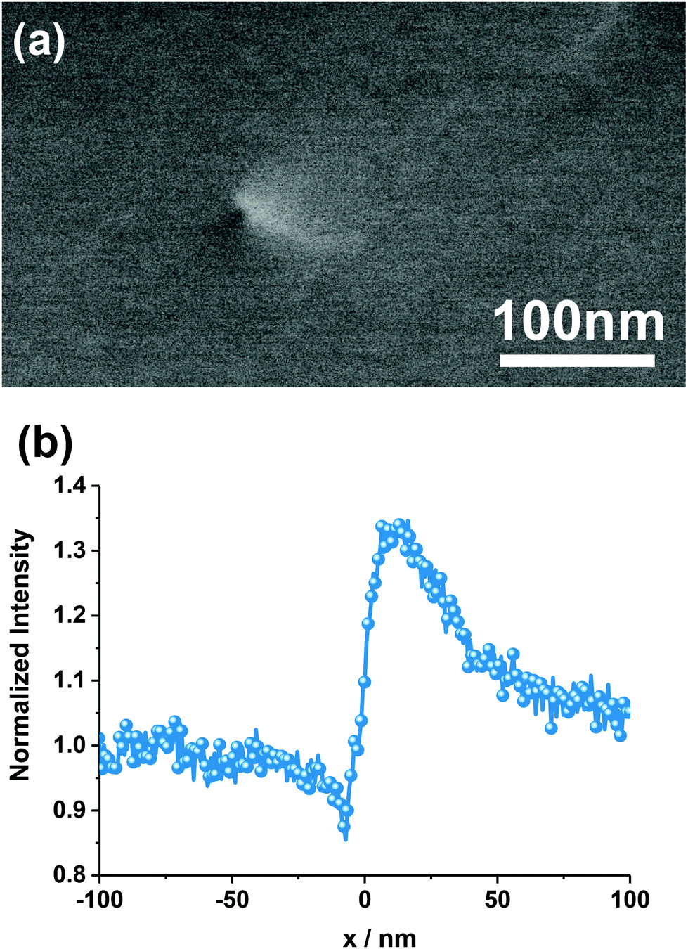 | ||
| Fig. 1 (a) ECCI micrograph obtained on a lowly defective SiGe buffer layer showing a single threading dislocation emerging at the layer surface. The typical contrast inversion across the defect is clearly visible. (b) Horizontal line section through the defect illustrating the contrast inversion quantitatively (i.e. transition from reduced backscatter signal to an increased backscatter signal when crossing the defect from left to right). | ||
To date, ECCI has been used to study threading dislocations on the surface of metals21 and various semiconductors such as SiC,22 GaSb23 and GaN.24,25 Moreover, buried misfit dislocations in SiGe/Si26 and various III/V compound heterostructures27,28 have been imaged successfully. However, thus far, ECCI has been limited to the characterization of defects in blanket layers or several micrometer wide mesa structures.29 In this study we apply ECCI for the first time successfully on deep sub-micron structures thereby enabling the non-destructive and quantitative visualization and characterization of crystalline defects in confined nanometer-scale structures relevant for future semiconductor device applications.
For this purpose, we used an Apreo SEM from Thermo Fisher equipped with a solid state concentric backscatter (CBS) detector mounted below the pole piece of the electron column. For optimum spatial resolution and signal-to-noise ratio we used beam energies between (5–20) keV and beam currents ranging from (0.4–3.2) nA. A magnetic immersion lens has been used to allow for maximum spatial resolution. To facilitate a precise alignment of the primary electron beam with the lattice planes of the sample, we selectively removed the STI oxide between the fins using buffered hydrofluoric acid (HF). Scanning the primary beam across the sample at low magnification enabled us to generate an electron channeling pattern (ECP) from the Si substrate (Fig. 2). Undesired interference effects caused by the interaction of the electron beam with the nanoscale fin structures on the substrate have been suppressed by moving the structures slightly out of the focal plane. Using sample tilt and rotation we then aligned the sample such that the center of the ECP (cross in Fig. 2) coincides with the transition between a Kikuchi line (dark line corresponding to a region of weak backscattering) and a Kikuchi band (bright band corresponding to a region of strong backscattering). In this way, when imaging at high magnification, the alignment condition providing the maximum defect contrast is ensured. In essence, the ECP greatly facilitates the selection of a certain diffraction condition (i.e. diffraction vector g) in a controlled and reproducible manner.28
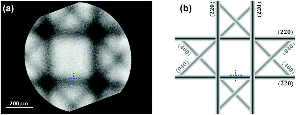 | ||
| Fig. 2 (a) Electron channeling pattern (ECP) obtained experimentally on a Si (001) substrate containing arrays of SiGe fin structures. The STI oxide between the fins has been removed selectively and the sample has been slightly moved out of focus to improve the visibility of the ECP while suppressing interference effects between the electron beam and the fin structures. (b) Indexed diagram corresponding to the ECP shown in (a). The selected diffraction condition corresponding to g = [−2−20] is indicated by the blue cross. | ||
It is important to realize that the visibility of an extended defect in ECCI critically depends on the Burgers vector b of the defect as well as the selected diffraction vector g. A dislocation for example will be invisible (and hence could not be detected using ECCI) if both extinction rules (1) g·b = 0 and (2) g·(b × u) = 0 would be fulfilled simultaneously (where u corresponds to the dislocation line direction). In the case of SiGe (and all face-centered cubic and diamond crystals) grown at rather low temperature, dislocations glide along the {111} planes in the 〈101〉 direction with a Burgers vector given by  〈101〉 (with a being the lattice parameter).30,31 As such, they can be classified as mixed dislocations whose Burgers vector consists of an edge and a screw component pointing in the two orthogonal 〈110〉 directions, respectively. Hence, for mixed dislocations and the selected diffraction condition g = [−2−20] (Fig. 2) visibility is always ensured since g·b ≠ 0. Nevertheless, the line direction u of the threading dislocation (the part of the dislocation which runs from the interface up to the surface of the epitaxial structure) can vary along its length and can differ for different threading arms, thereby leading to a variation of the edge/screw ratio. The latter could lead to a different channeling contrast observable with ECCI but as g·b remains unequal zero the dislocation will always be visible. It is worthwhile to note, however, that for the selected diffraction vector g = [−2−20], pure edge or pure screw dislocations with a Burgers vector oriented along [1−10] or [−110] would be invisible since g·b = 0. Hence, in order to capture pure edge or pure screw dislocations oriented along both orthogonal 〈110〉 directions, one would have to perform at least two measurements using e.g. two orthogonal diffraction vectors or alternatively choose a diffraction vector which is not perpendicular to any of the Burgers vectors in the sample (e.g.g = [400]).
Results and discussion
In the first experiment, we acquired an ECCI micrograph (Fig. 3) on a several micrometer large area, which was fabricated by selective epitaxial growth of Si0.3Ge0.7 into a large opening in the STI. Since the lateral dimensions of that area are much larger than the layer thickness (∼200 nm as-grown), no defect trapping occurs and the structure is therefore equivalent to a blanket layer. Since the layer thickness exceeds the critical thickness and elastic relaxation can be excluded given the large lateral dimensions of the pad, the layer must be plastically relaxed. Indeed, the Si0.3Ge0.7 peak position (∼3900 arcsec) in the (004) ω–2θ high-resolution X-ray diffraction (HRXRD) scan confirms the high degree of strain relaxation (Fig. 4).32,33 Plastic relaxation is associated with misfit dislocations at the buried layer–substrate interface whereby the misfit dislocations accommodate the lattice mismatch between both materials in the direction perpendicular to the dislocation line.34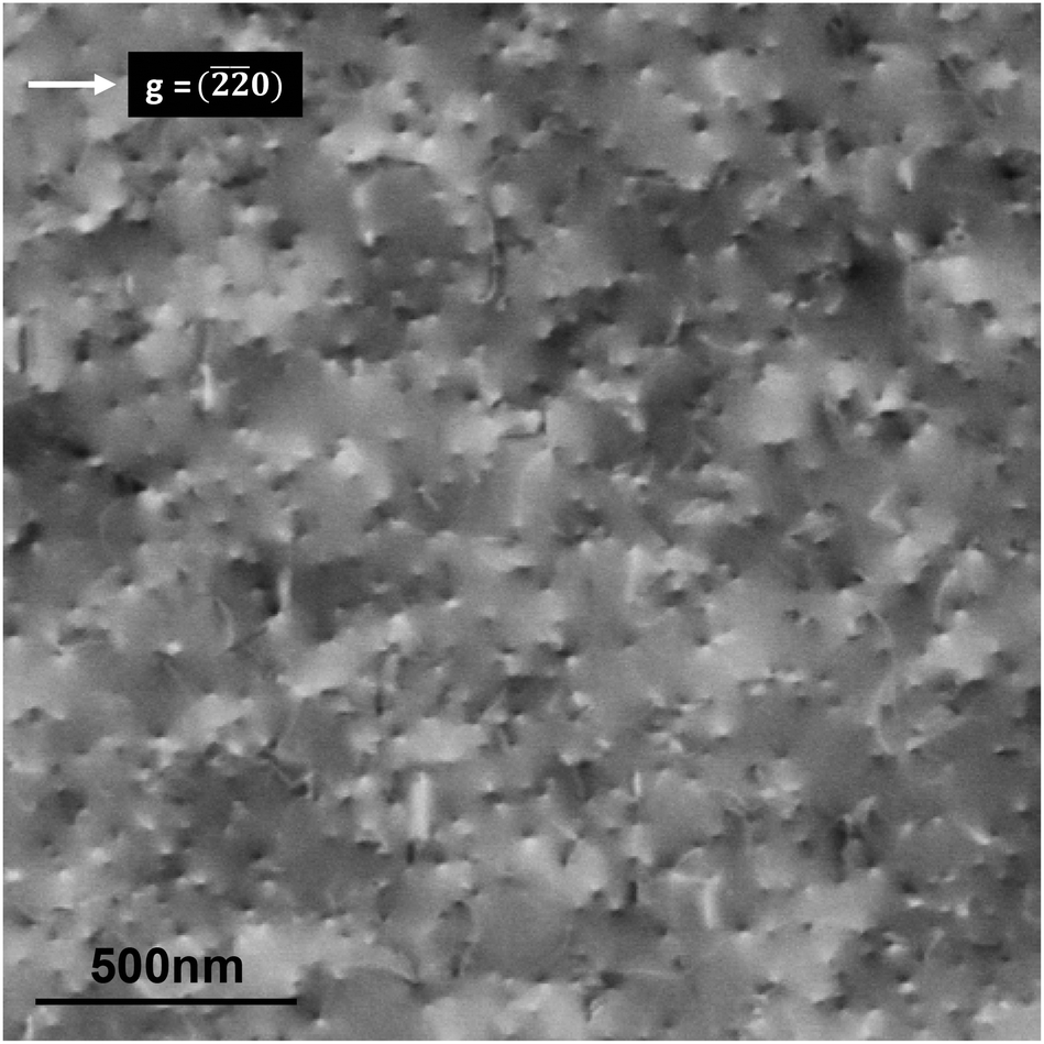 | ||
| Fig. 3 ECCI micrograph obtained on a Si0.3Ge0.7 layer grown into a several micrometer large window. The selected diffraction condition (cf.Fig. 2) is indicated by the arrow in the upper left corner of the graph. The same diffraction condition and hence g vector have been used throughout the paper for all ECCI micrographs. Individual threading dislocations are clearly resolved. The layer exhibits a threading dislocation density of ∼1010 cm−2. | ||
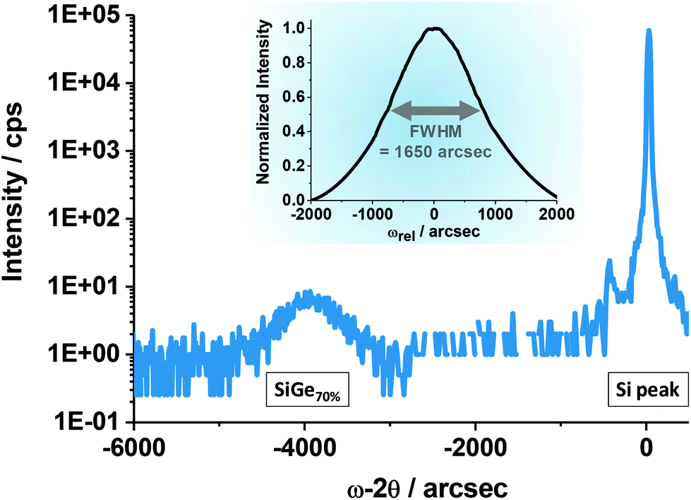 | ||
| Fig. 4 HRXRD (004) ω–2θ scan acquired on the large Si0.3Ge0.7 pad. The peak around −3900 arcsec corresponds to fully relaxed Si0.3Ge0.7. The inset shows an ω rocking curve obtained around the SiGe layer peak. The pronounced peak broadening with a FWHM value of 1650 arcsec is due to the high defect density and the associated mosaicity of the material. | ||
The misfit dislocations at the interface are finite in length; their ends typically curve upwards where they intersect with the layer surface. These upward segments are called threading dislocations. As long as these threading dislocation arms do not annihilate or get trapped at boundaries, they extend through the entire layer along the (111) planes until they terminate at the layer surface.35
The stress fields associated with these threading dislocations cause a local deformation of the crystal lattice planes, which can be imaged using ECCI, as described in the Experimental section. As a consequence, each of the dot-like features visible in the ECCI micrograph shown in Fig. 3 can be attributed to a single threading dislocation intersecting with the layer surface. The number of these features and hence the density of threading dislocations on the surface can now be extracted straightforwardly, resulting in a value of 1010 cm−2. The overall contrast variations which become apparent from the ECC image in Fig. 3 are due to the mosaicity and the associated lattice tilt of the material, which is caused by the high density of threading dislocations. The mosaicity and hence limited lateral coherence length of the layer causes a significant broadening of the HRXRD ω-rocking curve (inset Fig. 4). It has been demonstrated that from this peak broadening, the threading dislocation density can be estimated for the case of highly defective materials.36 Using the model of Ayers36 and a full width at half maximum (FWHM) of 1650 arcsec (inset Fig. 4) we could derive a threading dislocation density of 9.5 × 109 cm−2, which is in good agreement with the aforementioned defect density obtained from the ECCI micrograph shown in Fig. 3.
Next, we imaged 460 nm wide fin structures which have an aspect ratio AR (height![[thin space (1/6-em)]](https://www.rsc.org/images/entities/char_2009.gif) :width) of ∼0.4. Given the low AR, one does not expect an effective trapping of threading arms at the trench sidewalls during the selective epitaxial growth. Indeed, we observed a high density of threading dislocations terminating at the fin surface as can be seen in the ECCI micrographs displayed in Fig. 5. We extracted again a density equal to 1010 cm−2. In the magnified image, single threading dislocations (labeled with green arrows) can be observed in detail and the contrast inversion phenomenon discussed in the Experimental section of the paper can be clearly seen.
:width) of ∼0.4. Given the low AR, one does not expect an effective trapping of threading arms at the trench sidewalls during the selective epitaxial growth. Indeed, we observed a high density of threading dislocations terminating at the fin surface as can be seen in the ECCI micrographs displayed in Fig. 5. We extracted again a density equal to 1010 cm−2. In the magnified image, single threading dislocations (labeled with green arrows) can be observed in detail and the contrast inversion phenomenon discussed in the Experimental section of the paper can be clearly seen.
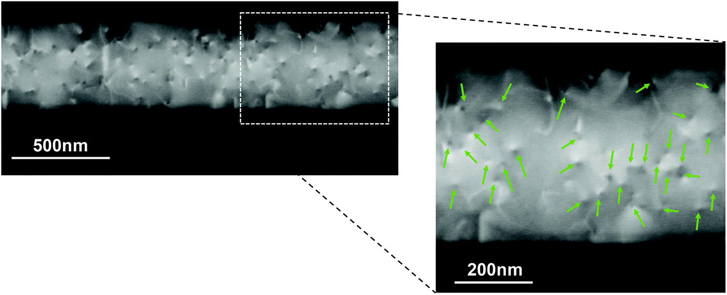 | ||
| Fig. 5 ECCI micrograph acquired on a 460 nm wide selectively grown SiGe fin. Individual threading dislocations are indicated by green arrows in the zoomed image. Similar to the blanket case (Fig. 3), a threading dislocation density of ∼1010 cm−2 could be extracted. | ||
For verification purposes we additionally performed TEM analysis on a specimen prepared along the length axis of a 460 nm wide fin. The cross-section TEM image in Fig. 6a confirms the high density of threading dislocations, though it is difficult to precisely quantify the number of threading arms reaching the fin surface due to the projection and overlap of the various defects present throughout the thickness of the TEM specimen. We furthermore applied wet chemical defect etching using the so-called Secco etch solution37, which consists of a solution of the Cr(VI) oxidant and the chemical dissolving agent HF in water. Diluted solutions were used in order to obtain sufficiently low etch rates to avoid overlapping etch pits associated with nearby defects. The density of etch pits was quantified using top-view SEM analysis (Fig. 6b) and confirmed the defect density determined by ECCI (Fig. 5) and hence the validity and accuracy of our approach.
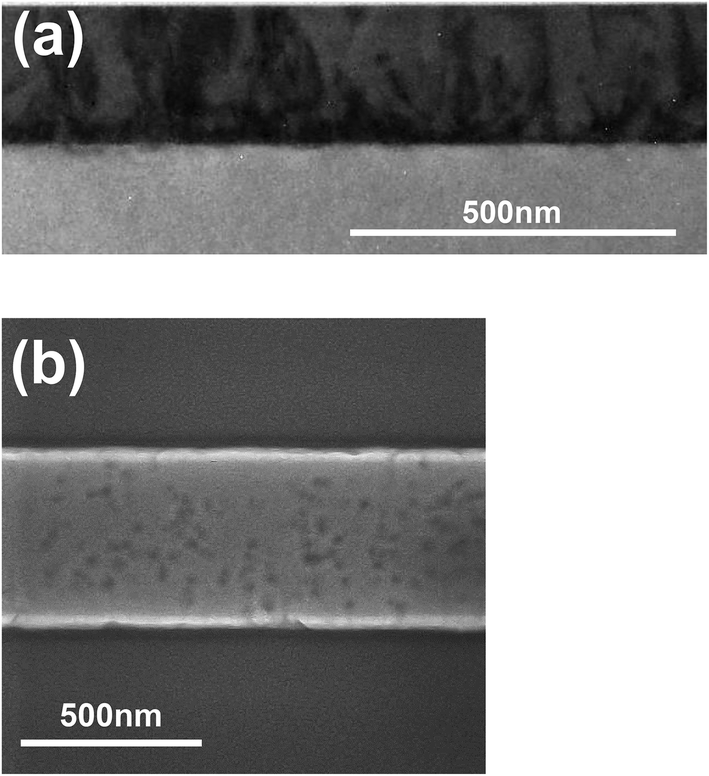 | ||
| Fig. 6 (a) TEM image acquired on a lamella prepared parallel to a 460 nm wide fin confirming a high density of threading dislocations. (b) Top-view SEM image after decorating the threading dislocations using Secco etch leading to the formation of etch pits at the defect sites. The density of etch pits is in agreement with the defect density extracted from ECCI analysis (Fig. 5). | ||
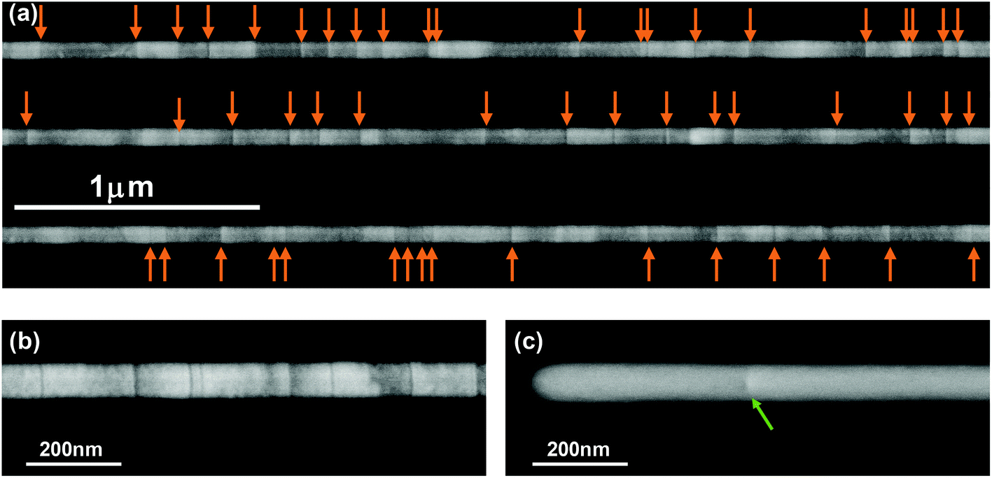
The picture changed upon decreasing the width of the selectively grown fins. While we could still observe a threading dislocation density of ∼1010 cm−2 on the surface of 260 nm wide fins, fewer threading dislocations (labeled with green arrows) reach the fin surface once the fin width is reduced to 170 nm and below (Fig. 7). In fact, for the 170 nm wide fins, we determined a reduction of the threading dislocation density to 6 × 109 cm−2 and for the 120 nm wide fins to 4 × 109 cm−2. At the same time, however, we detected an increasing number of line-like features on the fin surface when decreasing the fin width. These lines (highlighted by orange arrows in Fig. 7, 8 and 10) are oriented perpendicular to the fin length and they correspond to planar defects emerging at the fin surface as will be discussed further below.
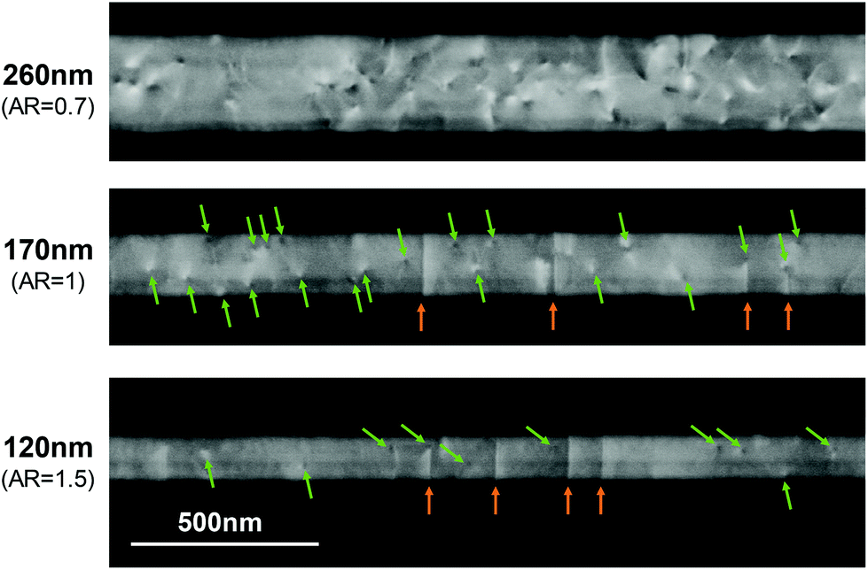 | ||
| Fig. 7 Top-view ECCI micrographs obtained on selectively grown SiGe fins of different widths. The density of threading dislocations reduces with decreasing fin width resulting in an effective threading dislocation density of 4 × 109 cm−2 for the 120 nm wide fins. At the same time, however, the number of planar defects (stacking faults) emerging at the fin surface increases. The fins’ aspect ratios AR (height:width) are indicated as well. | ||
 | ||
| Fig. 8 (a) Overview ECCI micrograph obtained on 75 nm wide (AR = 2.3) selectively grown SiGe fins at lower magnification, which allows for the non-destructive and fast determination of statistically relevant numbers on the density of planar defects (stacking faults, highlighted by orange arrows). In the presented case, a linear density of 44 planar defects per 10 μm fin length could be extracted. (b) ECCI micrograph of the same fin at higher magnification. Threading dislocations as observed for wider fins could not be detected. (c) ECCI micrograph acquired on a fin of similar dimensions which has been etched from a plastically relaxed blanket Ge layer. A single threading dislocation (highlighted by a green arrow) on the fin surface can be easily resolved. | ||
In the case of 75 nm wide fins (AR = 2.3), we could not observe any threading dislocation reaching the fin surface (Fig. 8a/b) whereby we inspected a fin surface area equal to 3.4 μm2 in total, out of which a representative part is shown in Fig. 8a. Hence, the threading dislocation density for fins of this dimension must be below 3 × 107 cm−2 if one assumes a uniform defect distribution. In this regard one must realize that in order to ascertain a defect density as low as e.g. 105 cm−2 (i.e. one threading dislocation per 1000 μm2 on average) one needs to inspect a fin surface area of several thousand μm2 in order to obtain statistically relevant information. We are currently extending our setup to enable automated measurements to facilitate the inspection of such large areas thereby achieving better statistics and hence a lower overall detection limit.
To verify the sensitivity of our method towards the detection of a single threading dislocation in such a confined volume, we furthermore analyzed fins were made by etching a lithographically defined pattern from a plastically relaxed blanket Ge layer grown on a Si (001) substrate. In this case of blanket layer growth and subsequent fin patterning, no defect trapping can occur and hence one must find threading arms on the surface of such fin structures in line with the defect density of the initial blanket layer. The ECCI micrograph shown in Fig. 8c has been acquired on such an etched fin structure ∼85 nm in width and clearly reveals a single threading dislocation emerging at the fin surface. This demonstrates the capability of ECCI to spatially resolve the lattice distortion induced by a single threading dislocation in such a narrow nanoscale 3D fin structure.
The threading dislocation densities obtained on the selectively grown SiGe fin structures of varying fin width (and hence aspect ratio AR) are summarized quantitatively in Fig. 9. The reason for the observed reduction in threading dislocation density for larger aspect ratios can be attributed to the aspect ratio trapping mechanism.16 Threading dislocations are connected to misfit dislocation lines in the (001) plane at the trench bottom (i.e. Si/SiGe interface) and they move towards the fin surface in the {111} planes. Since the angle between any {111} plane and the bottom of the trench (i.e. (001) plane) equals 54.7° in the case of a cubic crystal, any threading arm originating from the trench bottom and rising up in a (1![[1 with combining macron]](https://www.rsc.org/images/entities/char_0031_0304.gif) 1) or (1) plane will be blocked by the STI sidewalls if the aspect ratio of the trench exceeds
1) or (1) plane will be blocked by the STI sidewalls if the aspect ratio of the trench exceeds  . From Fig. 9 it becomes apparent that the threading dislocation density indeed drops significantly once the AR exceeds
 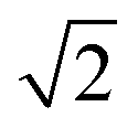 , although those threading arms rising upwards in the (111) or (11) planes (which do not intersect the STI sidewalls) can in principle still reach the fin surface. However, the line direction of such a threading arm typically has a non-zero component in the [10] direction (i.e. towards the STI sidewall). Hence, upon further increasing the trench's aspect ratio, the probability for these threading arms to terminate at the STI sidewalls before reaching the fin surface increases, leading to a further reduction of the threading dislocation density on the fin surface.
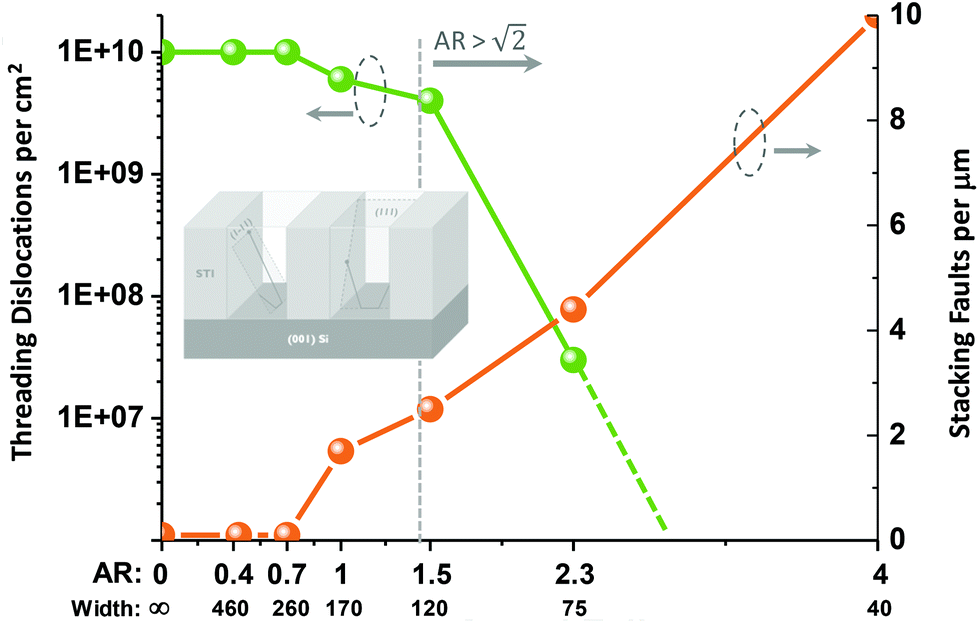 | ||
| Fig. 9 Areal density of threading dislocations (left y-axis) and the linear density of stacking faults (right y-axis) for fins of different widths as determined by ECCI. On the x-axis, the fin aspect ratio AR (height:width) as well as the fin width in nanometer are indicated. The inset schematically illustrates the trapping of threading dislocations at the STI sidewalls. | ||
As is already noted above, we furthermore identified line-like features on the surface of fins which are ≤170 nm in width (Fig. 7 and 8). As illustrated in Fig. 10, such a line in an ECCI micrograph can be explained by lattice distortions associated with planar defects such as stacking faults oriented parallel to the (111) or (11) planes emerging at the fin surface.
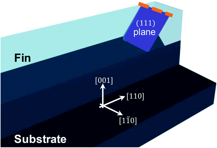 | ||
| Fig. 10 Schematic illustrating the positioning of a (111) plane in a fin oriented along the [110] direction. Planar defects such as stacking faults are plane-parallel to the {111} planes in a diamond crystal structure. Independent of the fin's aspect ratio, planar defects in the (111) and (11) plane (i.e. running perpendicular to the fin) are not trapped at the fin sidewall. The intersection of these planar defects with the fin top surface leads to a line-like feature (dashed orange line) oriented along the [10] direction. | ||
The formation of such stacking faults does not contribute to the accommodation of lattice mismatch in the case of SiGe/Si (001) heteroepitaxy, in contrast to the case of InP grown on Si (111).38 In both cases, however, the initial nucleation of the layer starts with the formation of small islands on the trench bottom. In the case of SiGe, the strain caused by the lattice mismatch can lead to an elastic deformation of the nucleation islands, which becomes more pronounced the larger the islands grow. Upon coalescence of these islands, stacking faults can form due to less perfect matching of the growth fronts of the islands at this position. The linear density of stacking faults for fins of different widths is summarized in Fig. 9. In contrast to the threading dislocation density, the number of planar defects increases for narrower trenches. This can be explained by the fact that the distance between nucleation islands is inversely related to the trench width,39 for which reason islands in narrower trenches can grow bigger and hence are more prone to elastic distortions before they coalesce. This leads to an increased probability for the formation of stacking faults in narrower trenches. Moreover, after coalescence of the various nucleation islands, stacking faults can also arise higher up in the trench due to irregularities (i.e. roughness) at the STI trench sidewalls.32,40 This mechanism can be neglected in wide structures, however, it becomes relevant in the case of narrower trenches exhibiting rougher sidewalls. Since the aspect ratio of these narrow trenches is higher than  , planar defects oriented parallel to the (11) or (1) planes are efficiently trapped by the STI sidewalls. Hence, only stacking faults running parallel to the (111) or (11) planes do reach the fin surface leading to the observed line-like features oriented along the [10] direction in the top-view ECCI micrographs. Besides, it is worthwhile to note that the described lines and hence the associated planar defects in the underlying fin can either cross the entire fin from one sidewall to the other or they extend only partially across the fin width (see e.g. the different line features highlighted by the orange arrows on top of the 170 nm wide fin in Fig. 7). In the latter case, the stacking fault is boarded by a partial dislocation.
In order to verify the origin of the line-like features observed by ECCI, we performed ECCI and subsequently cross-sectional STEM analysis on the very same fin structure (Fig. 11). Thereby, we could confirm an excellent correlation between planar defects emerging at the fin surface (as observed by cross-sectional STEM imaging – Fig. 11b) and the line-like features detected by ECCI (Fig. 11a).
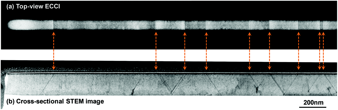 | ||
| Fig. 11 Correlation of (a) ECCI and (b) cross-sectional STEM analysis on the same selectively grown SiGe fin structure (75 nm wide, AR = 2.3). Each line-like feature in the top-view ECCI micrograph can be attributed to a stacking fault emerging at the surface of the SiGe fin. | ||
Moreover, to further support the aforementioned relationship between planar defect density and fin width (Fig. 9), we investigated selectively grown SiGe fins with widths down to 30 nm. From Fig. 12 it becomes apparent that using ECCI we are able to resolve stacking faults on the surface of these downscaled 3D fin structures. Thereby, we could ascertain a linear density of approximately 10 planar defects per micrometer fin length. We attribute this increase compared to the wider fins shown in Fig. 7 and 8a/b to the aforementioned increased size and hence elastic distortion of nucleation islands at the point of coalescence as well as the increased STI sidewall roughness in the case of the narrowest trenches.
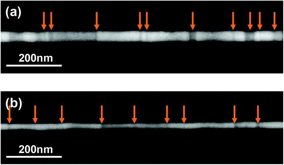 | ||
| Fig. 12 ECCI micrograph obtained on (a) 40 nm and (b) 30 nm wide selectively grown SiGe fin. A linear density of approximately 10 planar defects per micrometer fin length could be determined. | ||
Conclusion
We successfully imaged single dislocations and stacking faults in semiconductor fin structures with dimensions down to 30 nm using ECCI. For this purpose we mapped the intensity of electrons backscattered from the sample surface under controlled diffraction conditions using a SEM. The non-destructive nature of the approach enabled us to analyze deep sub-micron structures across large areas rapidly leading to excellent precision and low detection limit. We applied the method to nanometer-scale SiGe fin structures grown by selective epitaxy, whereby we could identify a strong impact of the structural dimensions on the nature and distribution of the defects. The presented observations and learnings exemplify that ECCI represents a powerful tool to characterize extended defects and hence the crystal quality of confined nanoscale 3D semiconductor device structures. As such, ECCI can aid in the development and optimization of epitaxial growth processes, thereby facilitating the introduction of emerging semiconductor technologies.Conflicts of interest
There are no conflicts to declare.Acknowledgements
The authors acknowledge the imec core CMOS program members for their support.References
- J. Mitard, L. Witters, Y. Sasaki, H. Arimura, A. Schulze, R. Loo, L.-A. Ragnarsson, A. Hikavyy, D. Cott, T. Chiarella, S. Kubicek, H. Mertens, R. Ritzenthaler, C. Vrancken, P. Favia, H. Bender, N. Horiguchi, K. Barla, D. Mocuta, A. Mocuta, N. Collaert and A.-Y. Thean, A 2nd Generation of 14/16nm-node compatible strained-Ge pFINFET with improved performance with respect to advanced Si-channel FinFETs, IEEE, 2016, pp. 1–2, DOI: 10.1109/VLSIT.2016.7573368 Search PubMed.
- R. Loo, A. Y. Hikavyy, L. Witters, A. Schulze, H. Arimura, D. Cott, J. Mitard, C. Porret, H. Mertens, P. Ryan, J. Wall, K. Matney, M. Wormington, P. Favia, O. Richard, H. Bender, A. Thean, N. Horiguchi, D. Mocuta and N. Collaert, ECS J. Solid State Sci. Technol., 2017, 6, P14–P20 CrossRef CAS.
- M. Heyns and W. Tsai, MRS Bull., 2009, 34, 485–492 CrossRef.
- S. Lourdudoss, Curr. Opin. Solid State Mater. Sci., 2012, 16, 91–99 CrossRef CAS.
- M. Paladugu, C. Merckling, R. Loo, O. Richard, H. Bender, J. Dekoster, W. Vandervorst, M. Caymax and M. Heyns, Cryst. Growth Des., 2012, 12, 4696–4702 CAS.
- E. Simoen, G. Eneman, A. Y. Hikavyy, R. Loo, S. Gupta, C. Merckling, A. Alian, A. Schulze, M. Caymax, R. Langer, K. Barla and C. Claeys, ECS Trans., 2015, 69, 119–130 CrossRef CAS.
- L. Souriau, T. Atanasova, V. Terzieva, A. Moussa, M. Caymax, R. Loo, M. Meuris and W. Vandervorst, J. Electrochem. Soc., 2008, 155, H677 CrossRef CAS.
- A. Abbadie, J.-M. Hartmann and F. Brunier, ECS Trans., 2007, 10, 3–19 CAS.
- J. L. Weyher and L. J. Giling, J. Appl. Phys., 1985, 58, 219–222 CrossRef CAS.
- D. J. Stirland, Appl. Phys. Lett., 1988, 53, 2432–2434 CrossRef CAS.
- J. L. Weyher, L. Macht, F. D. Tichelaar, H. W. Zandbergen, P. R. Hageman and P. K. Larsen, Mater. Sci. Eng., B, 2002, 91–92, 280–284 CrossRef.
- D. van Dorp, M. Mannarino, S. Arnauts, H. Bender, C. Merckling, A. Moussa, W. Vandervorst and A. Schulze, Crystals, 2017, 7, 98 CrossRef.
- D. Nam, J.-H. Kang, M. L. Brongersma and K. C. Saraswat, Opt. Lett., 2014, 39, 6205 CrossRef PubMed.
- M. Albrecht, J. L. Weyher, B. Lucznik, I. Grzegory and S. Porowski, Appl. Phys. Lett., 2008, 92, 231909 CrossRef.
- J. Bailey, E. Weber and J. Opsal, in Review of Progress in Quantitative Nondestructive Evaluation, ed. D. O. Thompson and D. E. Chimenti, Springer US, Boston, MA, 1989, pp. 1263–1271 Search PubMed.
- E. A. Fitzgerald and N. Chand, J. Electron. Mater., 1991, 20, 839–853 CrossRef CAS.
- I. Gutierrez-Urrutia, S. Zaefferer and D. Raabe, JOM, 2013, 65, 1229–1236 CrossRef.
- S. Zaefferer and N.-N. Elhami, Acta Mater., 2014, 75, 20–50 CrossRef CAS.
- A. J. Wilkinson and P. B. Hirsch, Micron, 1997, 28, 279–308 CrossRef.
- Y. N. Picard, M. Liu, J. Lammatao, R. Kamaladasa and M. De Graef, Ultramicroscopy, 2014, 146, 71–78 CrossRef CAS PubMed.
- I. Gutierrez-Urrutia and D. Raabe, Scr. Mater., 2012, 66, 343–346 CrossRef CAS.
- Y. N. Picard, M. E. Twigg, J. D. Caldwell, C. R. Eddy, P. G. Neudeck, A. J. Trunek and J. A. Powell, Appl. Phys. Lett., 2007, 90, 234101 CrossRef.
- Y. N. Picard, R. Kamaladasa, M. De Graef, N. T. Nuhfer, W. J. Mershon, T. Owens, L. Sedlacek and F. Lopour, Microsc. Today, 2012, 20, 12–16 CrossRef CAS.
- G. Naresh-Kumar, B. Hourahine, P. R. Edwards, A. P. Day, A. Winkelmann, A. J. Wilkinson, P. J. Parbrook, G. England and C. Trager-Cowan, Phys. Rev. Lett., 2012, 108, 135503 CrossRef CAS PubMed.
- G. Naresh-Kumar, B. Hourahine, A. Vilalta-Clemente, P. Ruterana, P. Gamarra, C. Lacam, M. Tordjman, M. A. di Forte-Poisson, P. J. Parbrook, A. P. Day, G. England and C. Trager-Cowan, Phys. Status Solidi A, 2012, 209, 424–426 CrossRef CAS.
- A. J. Wilkinson, G. R. Anstis, J. T. Czernuszka, N. J. Long and P. B. Hirsch, Philos. Mag. A, 1993, 68, 59–80 CrossRef CAS.
- A. J. Wilkinson, Philos. Mag. Lett., 1996, 73, 337–344 CrossRef CAS.
- S. D. Carnevale, J. I. Deitz, J. A. Carlin, Y. N. Picard, M. D. Graef, S. A. Ringel and T. J. Grassman, Appl. Phys. Lett., 2014, 104, 232111 CrossRef.
- A. J. Wilkinson, J. Electron Microsc., 2000, 49, 299–310 CrossRef CAS PubMed.
- P. M. Mooney, Mater. Sci. Eng., R, 1996, 17, 105–146 CrossRef.
- Y. B. Bolkhovityanov, O. P. Pchelyakov and S. I. Chikichev, Phys.-Usp., 2001, 44, 655–680 CrossRef CAS.
- A. Schulze, R. Loo, P. Ryan, M. Wormington, P. Favia, L. Witters, N. Collaert, H. Bender, W. Vandervorst and M. Caymax, Nanotechnology, 2017, 28, 145703 CrossRef CAS PubMed.
- A. Schulze, R. Loo, L. Witters, H. Mertens, A. Gawlik, N. Horiguchi, N. Collaert, M. Wormington, P. Ryan, W. Vandervorst and M. Caymax, Phys. Status Solidi C, 2017, 14(12), 1700156 Search PubMed.
- J. W. Matthews, J. Vac. Sci. Technol., 1975, 12, 126 CrossRef CAS.
- E. A. Fitzgerald, M. T. Currie, S. B. Samavedam, T. A. Langdo, G. Taraschi, V. Yang, C. W. Leitz and M. T. Bulsara, Phys. Status Solidi A, 1999, 171, 227–238 CrossRef CAS.
- J. E. Ayers, J. Cryst. Growth, 1994, 135, 71–77 CrossRef CAS.
- F. Secco d’ Aragona, J. Electrochem. Soc., 1972, 119, 948 CrossRef.
- A. Krost, F. Heinrichsdorff, D. Bimberg and H. Cerva, Appl. Phys. Lett., 1994, 64, 769–771 CrossRef CAS.
- S. Jiang, C. Merckling, A. Moussa, N. Waldron, M. Caymax, W. Vandervorst, N. Collaert, K. Barla, R. Langer, A. Thean, M. Seefeldt and M. Heyns, ECS J. Solid State Sci. Technol., 2015, 4, N83–N87 CrossRef CAS.
- G. Wang, M. R. Leys, N. D. Nguyen, R. Loo, G. Brammertz, O. Richard, H. Bender, J. Dekoster, M. Meuris, M. M. Heyns and M. Caymax, J. Electrochem. Soc., 2010, 157, H1023 CrossRef CAS.
Footnote |
| † Electronic supplementary information (ESI) available. See DOI: 10.1039/c8nr00186c |
| This journal is © The Royal Society of Chemistry 2018 |