
 Open Access Article
 This Open Access Article is licensed under a
 Creative Commons Attribution 3.0 Unported Licence
A single-molecule porphyrin-based switch for graphene nano-gaps†
Qingqing
Wu
,
Songjun
Hou
,
Hatef
Sadeghi
 * and
Colin J.
Lambert
*
* and
Colin J.
Lambert
*
Quantum Technology Centre, Lancaster University, LA1 4YB Lancaster, UK. E-mail: h.sadeghi@lancaster.ac.uk; c.lambert@lancaster.ac.uk
First published on 1st March 2018
Abstract
Stable single-molecule switches with high on–off ratios are an essential component for future molecular-scale circuitry. Unfortunately, devices using gold electrodes are neither complementary metal–oxide-semiconductor (CMOS) compatible nor stable at room temperature. To overcome these limitations, several groups have been developing electroburnt graphene electrodes for single molecule electronics. Here, in anticipation of these developments, we examine how the electrical switching properties of a series of porphyrin molecules with pendant dipoles can be tuned by systematically increasing the number of spacer units between the porphyrin core and graphene electrodes. The porphyrin is sandwiched between a graphene source and drain and gated by a third electrode. It is found that the system has two stable states with high and low conductances, which can be controlled by coupling the dipole of the functionalised porphyrin to an external electric field. The associated rotation leads to the breaking of conjugation and a decrease in electrical conductances. As the number of spacers is increased, the conductance ratio can increase from 100 with one spacer to 200 with four spacers. This switching ratio is further enhanced by decreasing the temperature, reaching approximately 2200 at 100 K. This design for a molecular switch using graphene electrodes could be extended to other aromatic systems.
Introduction
Single-molecule electronic devices have been investigated intensively both experimentally1–7 and theoretically,8–13 starting with the first molecular rectifier reported in 1974.14 Since that time a variety of tuneable transport properties and active functionalities have been investigated, including molecular switches.15–20 One example is the photo-switching operation of aryl azobenzene monolayer bridges between two vertical graphene sheets, whose conductance can be switched using optically induced length changes of the molecule.21 The second example involves redox-based switching, in which a molecule based on anthraquinone with a cross-conjugated structure is in the “off” state, whereas it is in the “on” state when it is reduced to linear conjugation.16 Another is based on conformational change, in which the conductance is tuned by decreasing the pi–pi orbital overlap within a bridging moiety by rotating adjacent phenyl rings.15,22 Recently, in an effort to overcome the limitations of gold electrodes for coming in contact with single molecules, graphene electroburnt nanogaps23–28 have been developed, which can be electrostatically tuned by a nearby buried gate electrode.29,30 This opens the way to the design of new molecular switches, which takes advantage of specific properties of such planar geometries.In the present paper, stimulated by the fact that conjugation can be broken by rotating two adjacent planar aromatic rings,15 we examine the possibility of single-molecule conductance switching when a single aromatic ring is rotated relative to the pi system of graphene electrodes. The target three-terminal device is shown in Fig. 1 and consists of a single porphyrin molecule placed in the nanogap between two graphene electrodes and simultaneously gated by a third electrode. When the porphyrin and graphene sheets are in the same plane, we expect the conductance to be high. When the plane of the porphyrin is perpendicular to the graphene plane, the conjugation will be broken and we expect the conductance to be low.
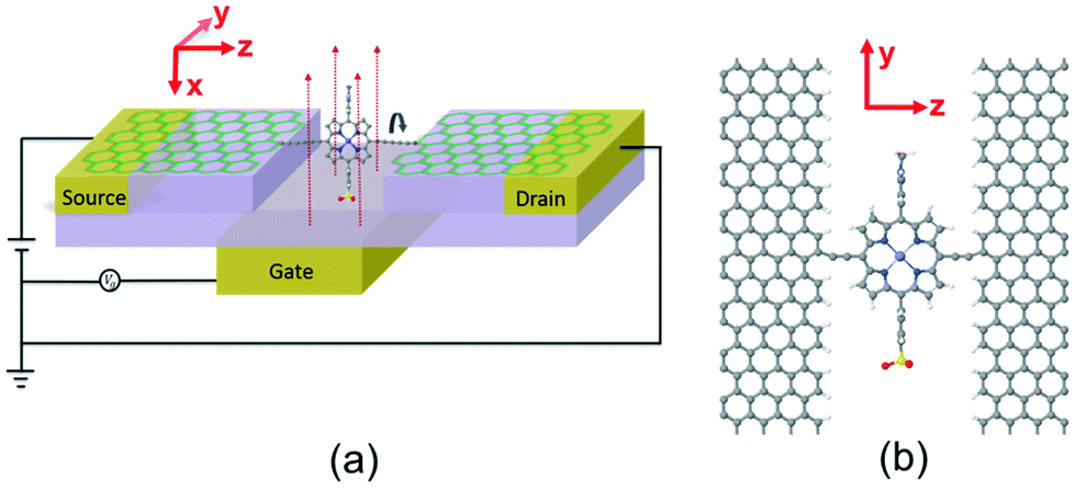 | ||
| Fig. 1 (a) Three terminal concept for nanoscale switch with source and drain and gate electrodes. (b) Schematic of the graphene/molecule/graphene device with one triple bond as a spacer. Graphene is terminated by hydrogen (white atoms). The red, yellow, and blue atoms represent oxygen, sulphur, and nitrogen, respectively. | ||
In the device shown in Fig. 1, the single porphyrin suspended in the graphene nano-gap contains pendant moieties, which create a dipole moment parallel to the plane of the porphyrin. The concept we aim to investigate is whether or not the porphyrin can be rotated by application of a modest electric field and whether or not this rotation creates a significant on–off ratio of the electrical conductance. In what follows, we demonstrate that there can be a huge difference in conductance between the zero-gate-voltage state and the device above a certain gate threshold value and therefore this combination of graphene electrodes and a porphyrin bridge is a promising design for a single-molecule switch. Crucially, it is possible to enhance the switching behaviour by increasing the separation between the graphene electrodes and functionalised porphyrin molecule. We demonstrate that the room temperature on–off conductance ratio can vary from 100 to 200 by increasing the number of C–C triple bonds from one to four, which act as spacers between porphyrin and graphene. We also demonstrate that the conductance ratio increases further from 200 to approximately 2200 by reducing the temperature to 100 K.
Results and discussion
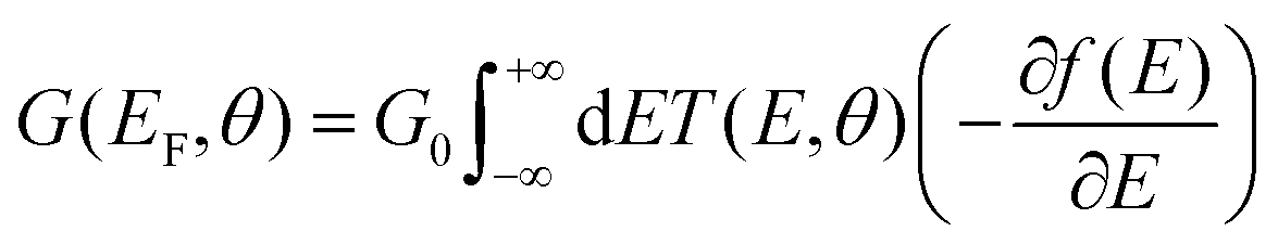
Fig. 1(b) shows a single porphyrin molecule functionalised with side groups which impart a dipole moment in the y direction, parallel to the plane of the porphyrin core. The latter is connected to two electroburnt graphene sheets via acetylene linkers. The separation between the two planar graphene sheets is d ≈ 1.3 nm and therefore they are electronically decoupled, except via the transport path through the porphyrin. Initially, as shown in Fig. 1, we consider only a single C–C triple bond spacer between each graphene electrode and the porphyrin. In our density functional theory (DFT) calculations, to avoid spurious edge effects, the structure is assigned periodic boundary conditions in the y direction.To understand the change in conductance due to a rotation θ about the axis of the triple bonds, we first compute the room-temperature electrical conductance (see Theoretical methods) when the porphyrin is frozen at a series of θ values between zero and 180°. Since the Fermi energy EF of the electrodes relative to the HOMO and LUMO levels could be tuned by doping or external gating, in Fig. 2(a) and (b), we plot graphs of room temperature ‘frozen’ zero-bias conductance G(EF,θ) versus EF for different values of θ. Fig. 2(a) shows the results for rotation angles θ between 0° and 90°, while Fig. 2(b) shows the results for θ between 90° and 180°. (The transmission spectra from which these conductances are derived are shown in Fig. S1 of the ESI.†) The results are plotted against EF − EDFTF, where EDFTF is the DFT-predicted Fermi energy. The junction in Fig. 1(b) is not exactly symmetric about a perpendicular plane passing through the triple bonds, and therefore G(EF,90° − θ) is almost, but not quite equal to G(EF,90° + θ). This slight asymmetry is due to the different structures of the dipole moieties –C6H4SO3, –NC5H4CH3 and the slight asymmetric connection to the graphene, imposed by the armchair edge. Clearly, there is a huge variation in G(EF,θ) as θ varies between 0° and 90°. Fig. 2(a and b) show that there are two main resonances at −1 eV and 0.5 eV for all angles except for 90°, where the conjugation between the pi system of porphyrin and the pi orbitals of graphene is broken. This broken conjugation at 90° leads to a low conductance over a range of Fermi energies in the vicinity of EDFTF. In order to gain insight into the origin of these resonances, Fig. 3 (left column) shows the local density of states (LDOS) in the vicinity of EDFTF, which is concentrated on the pendant moieties, whereas the right column shows that the LDOS at the transport resonance is around 0.3–0.5 eV, which is more delocalised across the backbone of the molecule. Similarly, the LDOS at −0.7 eV resonance is dominated by the pendant group, while that at −1 eV resonance is delocalised on the porphyrin core. The positions of the ‘delocalised’ resonances near 0.3–0.5 eV and −1 eV correspond to the LUMO and HOMO of the pure porphyrin molecule sandwiched in the graphene nano-gap (see Fig. S4 in ESI†), whose molecular orbitals are plotted in Fig. S2 of the ESI.†
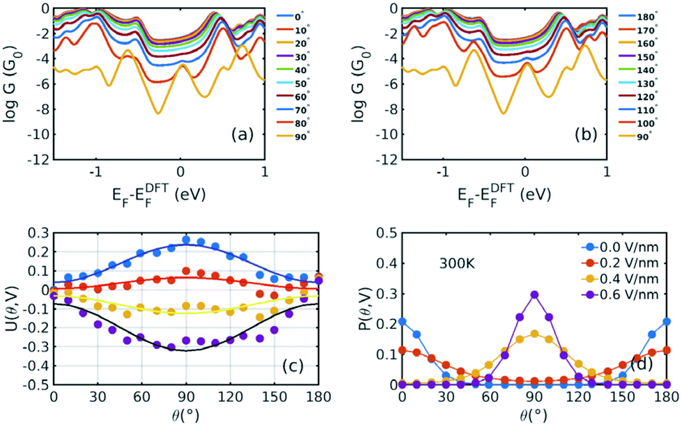 | ||
Fig. 2 Electrical conductances and energy landscapes of the device in Fig. 1b, with one triple bond on each side. (a), (b) For a series of fixed values of θ, these figures show room-temperature electrical conductances (in units of G0 = 2e2/h) without a gate electric field as a function of the Fermi level EF of the electrodes relative to the DFT-predicted value. (c) Potential energy versus θ for a series of perpendicular electric fields 0.0 V nm−1, 0.2 V nm−1, 0.4 V nm−1, and 0.6 V nm−1. The dots represent the total energies relative to the energy at 0° and 0 V nm−1 calculated by DFT, which are fitted by y = a![[thin space (1/6-em)]](https://www.rsc.org/images/entities/char_2009.gif) sin2θ + b. (d) The corresponding Boltzmann probability distribution (defined by eqn (2) and (3)) against θ under different gate electric fields at 300 K. The different structures corresponding to different rotating angles are not relaxed, because otherwise, upon relaxation, they would all relax back to the same minimum-energy angle. sin2θ + b. (d) The corresponding Boltzmann probability distribution (defined by eqn (2) and (3)) against θ under different gate electric fields at 300 K. The different structures corresponding to different rotating angles are not relaxed, because otherwise, upon relaxation, they would all relax back to the same minimum-energy angle. | ||
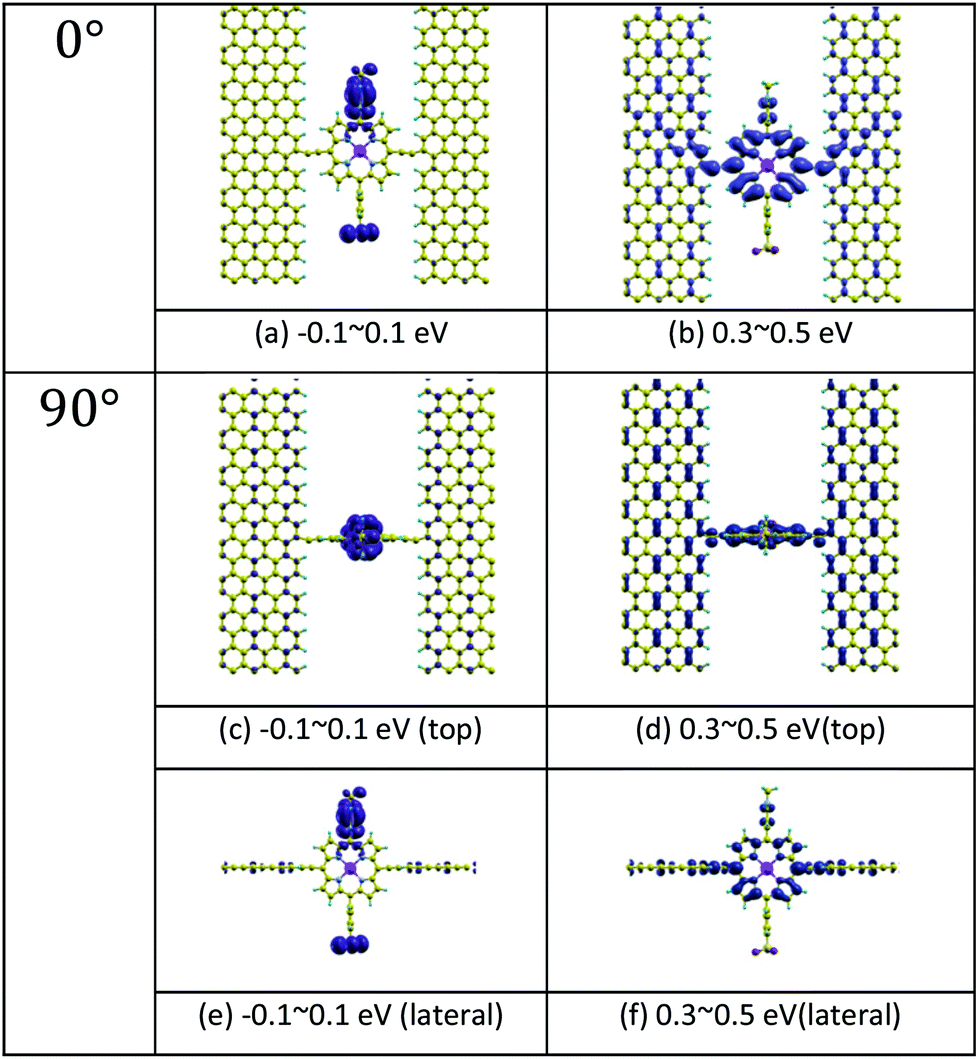 | ||
| Fig. 3 Local density of states (LDOS) of the junctions at 0° and 90° rotation angles. (a) and (b) show the LDOS in the energy windows −0.1–0.1 eV and 0.3–0.5 eV separately for 0°. (c) and (d) are for 90°. (e) and (f) are the lateral views for 90°. The energy windows refer to the DFT Fermi level in Fig. 2(a) and (b). Here, yellow atoms depict carbon atoms and light blue atoms depict hydrogen atoms. The LDOS is calculated by integrating the imaginary part of the Green's function G(r,E) with respect to energy E over a small energy window, centred of a particular energy. In the figure, results for two energy windows are presented, namely −0.1 eV to 0.1 eV and 0.3 eV to 0.5 eV. As shown in the figure, the orbitals within the first energy window are mainly located in the pendant groups, while the orbitals within the second energy window are localised on the porphyrin backbone. | ||
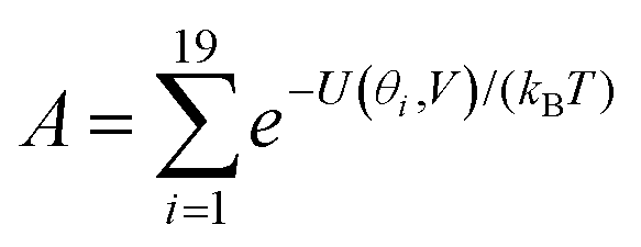
Fig. 2(a) and (b) show the conductance when a rotation angle θ is artificially imposed. In practice, the junction is controlled by imposing an external gate voltage V and at a finite temperature T, the rotation angle will fluctuate thermally. The probability of finding a given angle θ will be proportional to the Boltzmann factor e−U(θ,V)/(kBT), where U(θ,V) is the change in energy of the junction as a function of θ and V.31Fig. 2c shows the change of total energy U(θ,V) versus rotation angle θ with a series of gate voltages V. The dots in blue, red, yellow, and purple correspond to energy changes under perpendicular electric fields 0 V nm−1, 0.2 V nm−1, 0.4 V nm−1, and 0.6 V nm−1 obtained from the DFT calculation. These dots are fitted to the function y = asin2θ + b presented in solid lines, where b is an irrelevant constant, which disappears after normalising the Boltzmann weights, as shown in eqn (3). The blue line shows that in the absence of a gate field, the energy minimum occurs at θ = 0° and the maximum appears at 90°. On the other hand, the purple line shows that as the gate electric field increases, the energy minimum eventually switches from 0° to 90°. To compute each of the conductance curves of Fig. 2a and b, the rotation angle is constrained at a particular value of θ and the conductance is calculated using eqn (4). To determine the value of θ adopted by the switch at a given gate voltage V, the total energy U(θ,V) was computed for a series of angles θ and is plotted in Fig. 2c. At absolute zero and at a given gate voltage V, the switch would adopt the angle corresponding to the minimum of U(θ,V). However, at finite temperatures, the switch is subject to thermal fluctuations and will sample all angles. The probability distribution P(θ,V) that at a particular instant the switch will assume an angle θ is given by the Boltzmann distribution of eqn (2). For the single triple bond and different values of V, the room-temperature probability distributions are plotted in Fig. 2d and show that those angles corresponding to minima in U(θ,V) are sampled with the highest probability.
Fig. 4(a) shows the cos4θ relationship between the conductance and the rotation angle. Here, the Fermi level is chosen to be EF − EDFTF = −0.25 eV, which is close to the middle of the HOMO–LUMO gap. The cos4θ dependence arises, because the coupling to both the left and right graphene electrodes is proportional to cos2θ and the total conductance through the whole junction is proportional to the product of these couplings.8,32–34
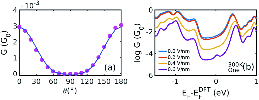 | ||
| Fig. 4 (a) Conductance versus the rotation angle derived from Fig. 2(a) and (b) at (EF − EDFTF = −0.25 eV). The pink dots are obtained from the DFT calculation and the blue solid line is the fitting curve by y = acos4θ + b. (b) Boltzmann-averaged conductances versus Fermi energy calculated using eqn (5) by averaging over the curves in Fig. 2(a) and (b), using the probability distributions in Fig. 2(d). | ||
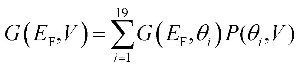
Fig. 4(b) illustrates the Boltzmann-averaged conductances obtained from eqn (5) for the series of perpendicular electric fields shown in Fig. 2(d). Specifically, the four average conductance curves shown in Fig. 4(b) are obtained based on the conductance curves in 2(a) and 2(b) of the 19 rotation angles and the distribution curves of the four electric fields in 2(d) according to eqn (5). This shows that for a wide range of Fermi energies within the HOMO–LUMO gap (more precisely, −0.4–0.4 eV), the conductance decreases approximately by two orders of magnitude due to the switching on of a 0.6 V nm−1 electric field and therefore this porphyrin-graphene device is a potential switch. On the other hand, an on–off conductance ratio of 100 (one specific value at a Fermi energy EF − EDFTF = −0.25 eV) in comparison with the gate electric field of 0 and 0.6 V nm−1 is not quite sufficient to be of technical interest and therefore we now demonstrate that this ratio can be improved by increasing the number of triple bonds connecting the porphyrin core to the graphene.
Fig. 5(a) shows a sketch of the device with two C–C triple bonds connecting the porphyrin to the graphene and Fig. 5(b) shows the corresponding energy landscape for four values of the perpendicular electric field ranging from 0.0 V nm−1 to 0.6 V nm−1. This series of calculations was repeated for junctions with three and four triple bonds connecting the porphyrin to each graphene electrode and in each case, a fit to the formula U(θ,V) = asin2θ + b was carried out. The energy landscapes for the structures with three and four triple bonds on each side are shown in Fig. S5 of the ESI.†Fig. 5(c) shows the plots of the barrier heights a when the perpendicular electric field is either zero (blue) or 0.6 V nm−1 (red). For the former, a is positive, corresponding to a maximum at θ = 90°, and the barrier decreases with the number of triple bonds. For the latter, a is negative, corresponding to a minimum at θ = 90° and the energy barrier increases with the number of triple bonds. In the absence of a gate voltage, it varies from about 0.2 eV for the single triple bond linker to 0.09 eV for the 4-triple bond linker. For comparison, kBT at room temperature is 0.025 eV. In the presence of a 0.6 V nm−1 gate field, it increases from about 0.25 eV for the single triple bond linker to 0.39 eV for the 4-triple bond linker. Since these are an order of magnitude greater than room temperature, switching is significant. Of course mathematically, for a large enough number of triple bonds, this trend should reverse and the energy barrier would tend to zero. However, in practice, the number of triple bonds is restricted by limits of synthetic chemistry, and therefore Fig. 5(c) suggests that this limit is not readily accessible.
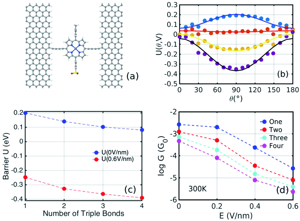 | ||
| Fig. 5 (a) Geometry of the switch with two carbon–carbon triple bonds on each side. (b) Potential landscape under different perpendicular electric fields. Similar plotting to Fig. 2(c). (c) Potential barrier extracted from the fitting curve as a function of the number of triple bonds on each contact. The blue one represents the energy barrier without gate while the red shows the potential well under 0.6 V nm−1. (d) Zero-bias, room-temperature conductance versus the external perpendicular electric field. The blue, red, cyan, and pink are for one, two, three, and four triple bonds structure. Here, the Fermi level is chosen to be near the centre of the HOMO–LUMO gap, at EF − EDFTF = −0.25 eV. | ||
Fig. 5(d) shows the Boltzmann-averaged conductances obtained at a Fermi energy EF − EDFTF = −0.25 eV near the middle of the HOMO–LUMO gap. As expected, the conductances decrease as the number of triple bonds increases, because transport takes place via phase-coherent tunneling.35 Furthermore, all conductances decrease with increasing electric field, because the most probable rotation angle switches from θ = 0° at low fields to θ = 90° at high fields. Fig. 5(d) shows that when the gate field 0.6 V nm−1 is imposed, the room-temperature conductance decreases by a factor of 100 for one triple bond, approximately 150 for two triple bonds, 185 for three, and 200 for four triple bonds (pink curve). This demonstrates that the on–off ratio can be increased significantly by increasing the length of the linkers between the porphyrin core and the electrodes.
Of course, as the length of the linkers increases, the synthetic chemistry becomes more challenging, and therefore to further increase the on–off ratio, we considered the effect of reducing the temperature. As shown in Fig. 6, reducing the temperature from 300 K to 100 K increases the on–off ratio from 100 to 1000 for one triple bond structure using the same electric field. This increase occurs, because in the presence of a 0.6 V nm−1 gate field, thermal fluctuations about the energy minimum are suppressed and therefore only low conductances near θ = 90° are sampled.
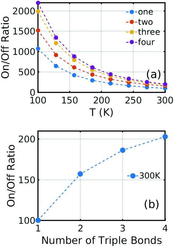 | ||
| Fig. 6 (a) On/off ratio evolution versus temperature T. The blue, orange, yellow, and purple are for one-triple bond, two triple bonds, three triple bonds, and four triple bonds structure, respectively. Here one, two, three, and four mean the number of triple bonds on each contact between the electrode and molecule. The corresponding curves at finite bias are presented in Fig. S6–5 of the ESI.† (b) On/off ratio evolution versus the number of triple bonds on each side. As an example, the on–off ratio of 100 for a single triple bond is obtained from Fig. 4b by comparing the conductance at one specific Fermi energy for a gate voltage of 0 with the corresponding value at a gate voltage of 0.6 V nm−1. In practice, the precise Fermi energy depends on the doping of the graphene, which in most experiments is hole doped. Therefore, the selected Fermi energy was chosen to be EF − EDFTF = −0.25 eV relative to the pristine value. | ||
Fig. 6(a) shows the on/off ratio evolution as a function of temperature. At infinite temperature, the on/off ratio would be, because all rotation angles would be sampled with equal probability, independent of the energy landscape. Fig. 6(b) shows the on/off ratio at room temperature, which increases from 100 to 200 when the number of triple bonds increases to four. Furthermore, from Fig. 6(a), at 100 K, the corresponding increase is from 1000 to 2200.
Theoretical methods
We used the DFT code SIESTA36 to obtain the optimized geometry adopting the generalised gradient approximation (GGA) and PBE functional37 for the exchange and correlation. We also chose a double-ζ plus polarized (DZP) basis set. Here, a large unit cell 50 × 51.12 in the x and y directions shown in Fig. 1(a) is adopted to avoid the electrostatic interaction between the dipole moieties due to periodic boundary conditions. For each angle θ, we then extracted the resulting mean-field Hamiltonian and overlap matrices and used them to compute the electrical properties of the devices with transport code Gollum.38 For a given angle θ, the transmission coefficient T(E,θ) for electrons as a function of energy E is calculated through the equations:| T(E,θ) = Tr[ΓL(E)G(E)ΓR(E)G†(E)] | (1) |
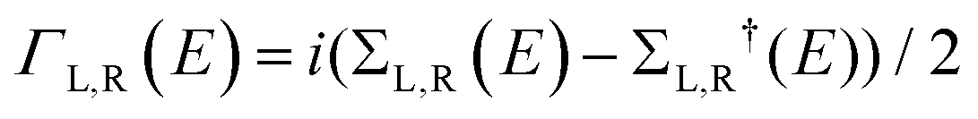 . ΓL,R determines the width of transmission resonances,
  are the self-energies describing the contact between the molecule and left (L) and right (R) electrodes. While G is the retarded Green's function of the molecule in the presence of the electrodes. The thermally-averaged conductance G(EF,V) is evaluated using the following formulae:
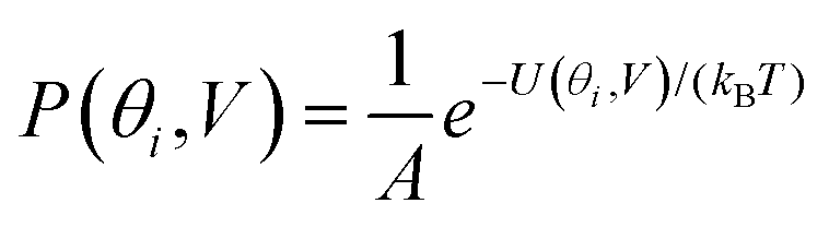 | (2) |
 | (3) |
 | (4) |
 | (5) |
Conclusions
In summary, using density functional theory combined with Green's function scattering techniques, we have computed the electrical conductance versus gate voltage of a porphyrin molecule sandwiched between two electro-burnt graphene electrodes. The porphyrin is connected to each electrode by oligoyne spacers formed from one to four triple bonds. Due to the presence of pendant moieties, which create an electric dipole moment, the gate voltage rotates the pi system of the porphyrin relative to the pi system of the graphene. For a rotation angle θ = 0, the pi systems are aligned and the conductance is high. For θ = 90°, the pi systems are orthogonal, the conjugation is broken, and the conductance is low. It is found that there exists a large conductance ratio between the on (θ = 90°) and off (θ = 0°) states, whose the room-temperature value ranges from approximately 100 for one-triple-bond spacers to 200 for four-triple-bond spacers. This on–off ratio can be further increased to 2200 by cooling the switch to 100 K. The above strategies for increasing the on–off ratio could be applied to other molecules with a conjugated core, connected to graphene electrodes by oligoyne linkers. To date, switches of the kind discussed in this paper have not been realised experimentally, but we are hopeful that our study will encourage progress in this direction. There are two possible junction-formation techniques, which could be used to create these switches. The first uses electroburning to produce graphene nanogaps of the required size,23,24,26 while the second uses ultrahigh-resolution electron-beam lithography and oxygen plasma ion etching.25 Interestingly, TEM images of such graphene junctions show that linear carbon chains can form at a variety of angles to the graphene edges, including the almost 90° bond angle assumed here.39Conflicts of interest
There are no conflicts to declare.Acknowledgements
Q. W. thanks James Thomas and Bart Limburg for the advice on the dipole group and also Steven Bailey and Iain Grace for discussions. H. S. acknowledges the Leverhulme Trust for Leverhulme Early Career Fellowship no. ECF-2017-186. This work was also supported by UK EPSRC (grant no. EP/N017188/1, EP/M014452/1, EP/N03337X/1 and EP/P027156/1).Notes and references
- C. Huang, S. Chen, K. Ørnsø, D. Reber, M. Baghernejad, Y. Fu, T. Wandlowski, S. Decurtins, W. Hong, K. S. Thygesen and S. X. Liu, Controlling Electrical Conductance through a Pi-Conjugated Cruciform Molecule by Selective Anchoring to Gold Electrodes, Angew. Chem., Int. Ed., 2015, 54(48), 14304–14307 CrossRef CAS PubMed.
- P. Moreno-García, M. Gulcur, D. Z. Manrique, T. Pope, W. Hong, V. Kaliginedi, C. Huang, A. S. Batsanov, M. R. Bryce, C. Lambert and T. Wandlowski, Single-molecule conductance of functionalized oligoynes: Length dependence and junction evolution, J. Am. Chem. Soc., 2013, 135(33), 12228–12240 CrossRef PubMed.
- K. Kim, T. H. Lee, E. J. G. Santos, P. S. Jo, A. Salleo, Y. Nishi and Z. Bao, Structural and Electrical Investigation of C 60 –Graphene Vertical Heterostructures, ACS Nano, 2015, 150608110504003 Search PubMed.
- Y. Kim, W. Jeong, K. Kim, W. Lee and P. Reddy, Electrostatic control of thermoelectricity in molecular junctions., Nat. Nanotechnol., 2014, 9(11), 881–885 CrossRef CAS PubMed.
- H. Vazquez, R. Skouta, S. Schneebeli, M. Kamenetska, R. Breslow, L. Venkataraman and M. S. Hybertsen, Probing the conductance superposition law in single-molecule circuits with parallel paths, Nat. Nanotechnol., 2012, 7(10), 663–667 CrossRef CAS PubMed.
- A. Xiang, H. Li, S. Chen, S.-X. Liu, S. Decurtins, M.-L. Bai, S. Hou and J. Liao, Electronic transport in benzodifuran single-molecule transistors, Nanoscale, 2015, 7, 7665–7673 RSC.
- B. Radisavljevic, A. Radenovic, J. Brivio, V. Giacometti and A. Kis, Single-layer MoS2 transistors, Nat. Nanotechnol., 2011, 6(3), 147–150 CrossRef CAS PubMed.
- C. J. Lambert, Basic concepts of quantum interference and electron transport in single-molecule electronics, Chem. Soc. Rev., 2015, 44(4), 875–888 RSC.
- H. Sadeghi, S. Sangtarash and C. J. Lambert, Oligoyne Molecular Junctions for Efficient Room Temperature Thermoelectric Power Generation, Nano Lett., 2015, 15(11), 7467–7472 CrossRef CAS PubMed.
- K. Ullmann, P. B. Coto, S. Leitherer, A. Molina-Ontoria, N. Martín, M. Thoss and H. B. Weber, Single-molecule junctions with epitaxial graphene nanoelectrodes, Nano Lett., 2015, 15(5), 3512–3518 CrossRef CAS PubMed.
- S. J. Heerema and C. Dekker, Graphene nanodevices for DNA sequencing, Nat. Nanotechnol., 2016, 11(2), 127–136 CrossRef CAS PubMed.
- Q. Wu, H. Sadeghi, V. M. García-Suárez, J. Ferrer and C. J. Lambert, Thermoelectricity in vertical graphene-C60-graphene architectures, Sci. Rep., 2017, 7, 11680 CrossRef PubMed.
- X.-F. Li, K.-Q. Chen, L. Wang and Y. Luo, Effects of Interface Roughness on Electronic Transport Properties of Nanotube−Molecule−Nanotube Junctions, J. Phys. Chem. C, 2010, 114(28), 12335–12340 CAS.
- A. Aviram and M. A. Ratner, Molecular rectifiers, Chem. Phys. Lett., 1974, 29(2), 277–283 CrossRef CAS.
- L. Venkataraman, J. E. Klare, C. Nuckolls, M. S. Hybertsen and M. L. Steigerwald, Dependence of single-molecule junction conductance on molecular conformation, Nature, 2006, 442(7105), 904–907 CrossRef CAS PubMed.
- E. H. Van Dijk, D. J. T. Myles, M. H. Van Der Veen and J. C. Hummelen, Synthesis and properties of an anthraquinone-based redox switch for molecular electronics, Org. Lett., 2006, 8(11), 2333–2336 CrossRef CAS PubMed.
- A. J. Kronemeijer, H. B. Akkerman, T. Kudernac, B. J. Van Wees, B. L. Feringa, P. W. M. Blom and B. De Boer, Reversible conductance switching in molecular devices, Adv. Mater., 2008, 20(8), 1467–1473 CrossRef CAS.
- R. Klajn, J. F. Stoddart and B. A. Grzybowski, Nanoparticles functionalised with reversible molecular and supramolecular switches, Chem. Soc. Rev., 2010, 39(6), 2203 RSC.
- N. Zhang, W.-Y. Lo, A. Jose, Z. Cai, L. Li and L. Yu, A Single-Molecular AND Gate Operated with Two Orthogonal Switching Mechanisms, Adv. Mater., 2017, 1701248, 1701248 CrossRef PubMed.
- Y. Cao, S. Dong, S. Liu, Z. Liu and X. Guo, Toward functional molecular devices based on graphene-molecule junctions, Angew. Chem., Int. Ed., 2013, 52(14), 3906–3910 CrossRef CAS PubMed.
- S. Seo, M. Min, S. M. Lee and H. Lee, Photo-switchable molecular monolayer anchored between highly transparent and flexible graphene electrodes, Nat. Commun., 2013, 4(May), 1920 CrossRef PubMed.
- N. Xin, J. Wang, C. Jia, Z. Liu, X. Zhang, C. Yu, M. Li, S. Wang, Y. Gong, H. Sun, G. Zhang, Z. Liu, G. Zhang, J. Liao, D. Zhang and X. Guo, Stereoelectronic Effect-Induced Conductance Switching in Aromatic Chain Single-Molecule Junctions, Nano Lett., 2017, 17(2), 856–861 CrossRef CAS PubMed.
- H. Sadeghi, S. Sangtarash and C. Lambert, Robust Molecular Anchoring to Graphene Electrodes, Nano Lett., 2017, 17(8), 4611–4618 CrossRef CAS PubMed.
- H. Sadeghi, J. Mol, C. Lau, A. Briggs, J. Warner and C. J. Lambert, Conductance enlargement in pico-scale electro-burnt graphene nanojunctions, Proc. Natl. Acad. Sci. U. S. A., 2015, 112(9), 2658–2663 CrossRef CAS PubMed.
- Y. Cao, S. Dong, S. Liu, L. He, L. Gan, X. Yu, M. L. Steigerwald, X. Wu, Z. Liu and X. Guo, Building high-throughput molecular junctions using indented graphene point contacts, Angew. Chem., Int. Ed., 2012, 51(49), 12228–12232 CrossRef CAS PubMed.
- F. Prins, A. Barreiro, J. W. Ruitenberg, J. S. Seldenthuis, N. Aliaga-Alcalde, L. M. K. Vandersypen and H. S. J. Van Der Zant, Room-temperature gating of molecular junctions using few-layer graphene nanogap electrodes, Nano Lett., 2011, 11(11), 4607–4611 CrossRef CAS PubMed.
- C. Nef, L. Pósa, P. Makk, W. Fu, A. Halbritter, C. Schönenberger and M. Calame, High-yield fabrication of nm-size gaps in monolayer CVD graphene, Nanoscale, 2014, 6(13), 7249–7254 RSC.
- A. J. Bergren and O. Ivashenko, Carbon Electrodes in Molecular Electronics, in Electrochemistry of Carbon Electrodesm, ed. R. C. Alkire, P. N. Bartlett and J. Lipkowski, Wiley-VCH Verlag GmbH & Co. KGaA, Weinheim, Germany, 2015, DOI:10.1002/9783527697489.ch10.
- J. A. Mol, C. S. Lau, W. J. M. Lewis, H. Sadeghi, C. Roche, A. Cnossen, J. H. Warner, C. J. Lambert, H. L. Anderson and G. A. D. Briggs, Graphene-porphyrin single-molecule transistors, Nanoscale, 2015, 7(31), 13181–13185 RSC.
- P. Gehring, J. K. Sowa, J. Cremers, Q. Wu, H. Sadeghi, Y. Sheng, J. H. Warner, C. J. Lambert, G. A. D. Briggs and J. A. Mol, Distinguishing Lead and Molecule States in Graphene-Based Single-Electron Transistors, ACS Nano, 2017, 11(6), 5325–5331 CrossRef CAS PubMed.
- H. Sadeghi, S. Sangtarash, Q. Al-Galiby, R. Sparks, S. Bailey and C. J. Lambert, Negative differential electrical resistance of a rotational organic nanomotor, Beilstein J. Nanotechnol., 2015, 6(1), 2332–2337 CrossRef CAS PubMed.
- J. S. Seldenthuis, F. Prins, J. M. Thijssen and H. S. J. Van Der Zant, An all-electric single-molecule motor, ACS Nano, 2010, 4(11), 6681–6686 CrossRef CAS PubMed.
- C. M. Finch, S. Sirichantaropass, S. W. Bailey, I. M. Grace, V. M. García-Suárez and C. J. Lambert, Conformation dependence of molecular conductance: Chemistry versus geometry, J. Phys.: Condens. Matter, 2008, 20, 022203 CrossRef.
- M. Bürkle, J. K. Viljas, D. Vonlanthen, A. Mishchenko, G. Schön, M. Mayor, T. Wandlowski and F. Pauly, Conduction mechanisms in biphenyl dithiol single-molecule junctions, Phys. Rev. B: Condens. Matter Mater. Phys., 2012, 85(7), 1–12 CrossRef.
- A. Al-Backri, V. Zólyomi and C. J. Lambert, Electronic properties of linear carbon chains: Resolving the controversy, J. Chem. Phys., 2014, 140, 104306 CrossRef PubMed.
- J. M. Soler, E. Artacho, J. D. Gale, A. Garcìa, J. Junquera, P. Ordejòn and D. Sànchez-Portal, SIESTA Method For Ab Initio Order-N Materials Simulation, J. Phys.: Condens. Matter, 2002, 14(11), 2745–2779 CrossRef CAS.
- J. P. Perdew, K. Burke and M. Ernzerhof, Generalized Gradient Approximation Made Simple- ERRATA, Phys. Rev. Lett., 1996, 77(18), 3865–3868 CrossRef CAS PubMed.
- J. Ferrer, C. J. Lambert, V. M. García-Suárez, D. Zs. Manrique, D. Visontai, L. Oroszlany, R. Rodríguez-Ferradás, I. Grace, S. W. D. Bailey, K. Gillemot, H. Sadeghi and L. A. Algharagholy, GOLLUM: A next-generation simulation tool for electron, thermal and spin transport, New J. Phys., 2014, 16, 093029 CrossRef.
- Y.-C. Lin, S. Morishita, M. Koshino, C.-H. Yeh, Po.-Y. Teng, Po.-W. Chiu, H. Sawada and K. Suenaga, Unexpected Huge Dimerization Ratio in One-Dimensional Carbon Atomic Chains, Nano Lett., 2017, 17(1), 494–500 CrossRef CAS PubMed.
Footnote |
| † Electronic supplementary information (ESI) available. See DOI: 10.1039/c8nr00025e |
| This journal is © The Royal Society of Chemistry 2018 |