
 Open Access Article
 This Open Access Article is licensed under a Creative Commons Attribution-Non Commercial 3.0 Unported Licence
Large-scale fabrication of free-standing and sub-μm PDMS through-hole membranes†
Hai
Le-The
 *,
Martijn
Tibbe
,
Joshua
Loessberg-Zahl
,
Marciano
Palma do Carmo
,
Marinke
van der Helm
,
Johan
Bomer
,
Albert
van den Berg
,
Anne
Leferink
,
Loes
Segerink
and
Jan
Eijkel
*,
Martijn
Tibbe
,
Joshua
Loessberg-Zahl
,
Marciano
Palma do Carmo
,
Marinke
van der Helm
,
Johan
Bomer
,
Albert
van den Berg
,
Anne
Leferink
,
Loes
Segerink
and
Jan
Eijkel
BIOS Lab-on-a-Chip Group, MESA + Institute for Nanotechnology, MIRA Institute for Biomedical Technology and Technical Medicine, Max Planck Center for Complex Fluid Dynamics, University of Twente, 7522 NB Enschede, The Netherlands. E-mail: h.lethe@utwente.nl
First published on 16th April 2018
Abstract
Free-standing polydimethylsiloxane (PDMS) through-hole membranes have been studied extensively in recent years for chemical and biomedical applications. However, robust fabrication of such membranes with sub-μm through-holes, and at a sub-μm thickness over large areas is challenging. In this paper, we report a robust and simple method for large-scale fabrication of free-standing and sub-μm PDMS through-hole membranes, combining soft-lithography with reactive plasma etching techniques. First, arrays of sub-μm photoresist (PR) columns were patterned on another spin-coated sacrificial PR layer, using conventional photolithography processes. Subsequently, a solution of PDMS![[thin space (1/6-em)]](https://www.rsc.org/images/entities/char_2009.gif) :hexane at a 1:10 ratio was spin-coated over these fabricated arrays. The cured PDMS membrane was etched in a plasma mixture of sulfur hexafluoride (SF6) and oxygen (O2) to open the through-holes. This PDMS membrane can be smoothly released with a supporting ring by completely dissolving the sacrificial PR structures in acetone. Using this fabrication method, we demonstrated the fabrication of free-standing PDMS membranes at various sub-μm thicknesses down to 600 ± 20 nm, and nanometer-sized through-hole (810 ± 20 nm diameter) densities, over areas as large as 3 cm in diameter. Furthermore, we demonstrated the potential of the as-prepared membranes as cell-culture substrates for biomedical applications by culturing endothelial cells on these membranes in a Transwell-like set-up.
:hexane at a 1:10 ratio was spin-coated over these fabricated arrays. The cured PDMS membrane was etched in a plasma mixture of sulfur hexafluoride (SF6) and oxygen (O2) to open the through-holes. This PDMS membrane can be smoothly released with a supporting ring by completely dissolving the sacrificial PR structures in acetone. Using this fabrication method, we demonstrated the fabrication of free-standing PDMS membranes at various sub-μm thicknesses down to 600 ± 20 nm, and nanometer-sized through-hole (810 ± 20 nm diameter) densities, over areas as large as 3 cm in diameter. Furthermore, we demonstrated the potential of the as-prepared membranes as cell-culture substrates for biomedical applications by culturing endothelial cells on these membranes in a Transwell-like set-up.
Introduction
Free-standing through-hole nanomembranes have attracted a great deal of attention over the past decade due to their wide range of applications1–4 including sterile filtration (bacteria and viruses), cell sorting, biomolecular separation, and biomimetic microfluidic devices, termed organs-on-a-chip systems, such as gut-on-a-chip,5 lung-on-a-chip6 and blood–brain barrier-on-a-chip.7 Such nanomembranes have been fabricated from various materials including silicon-based inorganic materials,8,9 and polymers.10–13 Nanomembranes made of silicon (Si) or silicon nitride (SiNx) can be fabricated at various thicknesses ranging from a few nanometers to a few hundreds of nanometers, possessing nano through-holes of a few tens of nanometers.8 However, fabrication of such through-hole nanomembranes requires dedicated patterning systems such as electron-beam lithography,14 laser interference lithography15 or focused ion-beam milling,16 which are expensive and labor intensive. Moreover, these inorganic nanomembranes are very fragile under applied pressure and mechanical contact, thus resulting in a difficulty to fabricate/handle large-scale areas. This also leads to a difficulty in the integration of fabricated nanomembranes with other micro/nanofluidic systems made of polydimethylsiloxane (PDMS) or glass/fused-silica. Nanomembranes made of polymers, e.g. PDMS, on the other hand have the advantages of being economic and easy to integrate into lab-on-a-chip systems.6,17–19 Due to its remarkable advantages of low costs, chemical resistance, flexibility, gas permeability, optical transparency, and high molding capability, PDMS has become one of the most widely used polymers in various fields, especially for lab-on-a-chip or micro total analysis systems.20 However, large-area fabrication of free-standing and sub-μm thick PDMS membranes with nanometer-sized through-holes has been considered challenging.A number of methods has been reported to fabricate PDMS through-hole membranes such as imprinting,21 manual punching,22 and spin-coating on SU-8 molds.23,24 However, these fabrication methods are each accompanied by their own drawbacks. The imprinting process involves pressing a positive pillar mold into a pre-polymer layer coated on a flat surface. The dependence of the required pressure on the pre-polymer viscosity however leads to the difficulty in reliably fabricating uniform PDMS nanomembranes over large areas. In addition, insufficient applied pressure could lead to undesirable closed holes rather than complete through-holes. A manual punching process involves punching a needle gauge through a continuous PDMS membrane, which is time consuming. Moreover, handling of membranes at the nanoscale for the punching process is rather difficult, thus making it not suitable for high-yield patterning PDMS through-hole nanomembranes over large footprints. A spin-coating process can be used, based on the coating of PDMS solution at a high spinning speed over a patterned SU-8 column array, resulting in a PDMS layer thinner than the column height. Subsequently demolding the cured PDMS layer from the SU-8 mold results in a PDMS through-hole membrane. However, the difficulty in the fabrication of SU-8 columns in sub-μm diameter ranges limits its use for fabricating PDMS membranes with nanometer-sized through-holes.
By using a hierarchical mold under applied pressure, Cho et al. reported the fabrication of flexible and free-standing nanomembranes made of ultraviolet-curable resins.25 Based on the dewetting of resins into a hierarchical mold, nanomembranes with various nano through-hole sizes from 50 nm to 800 nm, and shapes (dots or lines) were fabricated. By combining hierarchical structures with a microfluidic chip, Tahk et al.26 reported an alternative fabrication method for patterning multiscale PDMS through-hole membranes. Their chip was fabricated by plasma, bonding the top part of a microfluidic chip made of PDMS with a nanocolumn patterned substrate. Injecting a pre-polymer and subsequently curing the PDMS solution inside the microfluidic chip resulted in the formation of membranes with through-holes size ranging from a hundred nanometers to a hundred micrometers. By gently separating the chip bonding via cutting, sub-μm PDMS membranes with nano through-holes were peeled off from the PDMS chip. Although being able to fabricate free-standing and through-hole nanomembranes, these fabrication methods25,26 require hierarchical molds consisting of patterned nanocolumns. Patterning such molds is labor intensive, and requires dedicated patterning systems which are expensive. In addition, an additional coating of anti-sticking layers on the molds prior to the injection of the pre-polymer is needed in order to release the nanomembrane from the mold.
Recently, Kang et al. reported a compelling technique that allows rapidly patterning free-standing and continuous PDMS nanomembranes over large areas.27 Using a mixture solution of PDMS and hexane, PDMS nanomembranes with various thicknesses from 70 nm to a few hundreds of nanometers could be fabricated on a sacrificial photoresist (PR) layer by spin-coating at a very high speed of 6000 rpm. By gluing a thick PDMS ring used as a support on the membrane surface, and subsequently dissolving the PR layer in acetone, a free-standing and continuous PDMS nanomembrane supported on the PDMS ring was obtained over large areas up to 6 cm in diameter. The use of a PDMS support ring prevented the folding of this membrane, thus providing an opportunity to smoothly release the nanomembrane from the dissolved PR layer.
Further improving the fabrication technique reported by Kang et al.,27 we present a robust fabrication method that allows rapid patterning of free-standing PDMS membranes with periodic sub-μm through-holes with various sub-μm thicknesses. Our fabrication method combines the soft lithography technique with an easy operation reactive plasma etching technique, and thus is suitable for mass production at low cost. Using this method, we demonstrate the fabrication of free-standing and sub-μm PDMS membranes over large footprints of 3 cm in diameter, possessing periodic sub-μm through-holes of 810 ± 20 nm in diameter with different hole interspacings of 3 μm, 5 μm, and 10 μm. Additionally, we demonstrate the potential of this membrane as a cell-culture substrate for biomedical applications by culturing endothelial cells on these membranes in a Transwell-like set-up.
Experimental section
Patterning sub-μm photoresist column arrays on a sacrificial photoresist layer
Fig. 1 shows the process of fabricating free-standing and sub-μm PDMS through-hole membranes. A positive PR layer (OiR 907-17i, Fujifilm, Japan) of 1.71 ± 0.04 μm thickness destined as the sacrificial layer was spin-coated on a Si wafer (525 μm thick, Okmetic, Finland) at 4000 rpm for 30 s, followed by baking on a hot-plate at 95 °C for 2 min. Subsequently, an extremely thin titanium (Ti) layer (∼3 nm) was sputtered on the coated PR layer, using a DC sputtering system (in-house built T'COathy system, NanoLab)28 at a pressure of 6.6 × 10⁻³ mbar, and 200 W (Fig. 1a). This Ti layer was used to prevent the intermixing of the first PR layer with the second PR layer of approximately 1.7 μm, which was spin-coated at 4000 rpm for 30 s followed by baking on a hot-plate at 95 °C for 1 min (Fig. 1b). At this sputtered thickness a discontinuous Ti layer was obtained. Moreover, it is worth mentioning that an extremely thin layer of hexamethyldisilazane (HMDS) was spin-coated on the surface of the Ti-coated PR layer before spin-coating the second PR layer. This HMDS layer is used to increase the adhesion of patterned PR structures with the substrates.29 A photo-mask made of quartz containing arrays of 1 μm chromium (Cr) discs with three different pitches, i.e. 3 μm, 5 μm, and 10 μm, was fabricated in-house by using a mask-making system (DWL 2000 Laser Lithography System, Heidelberg Instruments, Germany). The exposure process was conducted by using a mask alignment system (EVG620, EV Group, Austria) for 3 s at an intensity of 12 mW cm−2, and in vacuum contact mode. The vacuum was always kept at 0.75 bar during the exposure process to ensure a good contact of the mask over the entire wafer, thus increasing the reproducibility of the fabrication process. Thereafter, the wafer was post-baked on a hot-plate at 120 °C for 15 s, followed by developing in an OPD4246 developer for 1 min, and rinsing with de-ionized (DI) water to complete the fabrication of sub-μm PR column arrays on another, sacrificial, PR layer (Fig. 1c).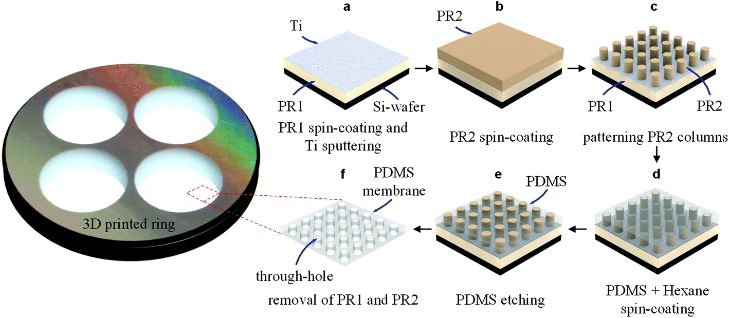 | ||
| Fig. 1 Fabrication process of a free-standing and sub-μm thick PDMS through-hole membrane. (a) PR1 was spin-coated on a Si-wafer, and a Ti layer was sputtered directly on the coated PR layer. (b, c) PR2 was coated and an array of sub-μm columns was patterned into this layer using conventional photolithography. (d) A solution of PDMS:hexane at a 1:10 ratio was spin-coated over the fabricated PR column array. (e) Plasma etching of the PDMS membrane was conducted in a reactive ion etching system to open the through-holes. (f) Releasing of the PDMS through-hole membrane in acetone using a 3D-printed ring as a support. | ||
Patterning sub-μm PDMS through-hole membranes
A solution of the PDMS prepolymer with the curing agent (10:1) was diluted with hexane at a 1:10 (PDMS:hexane) ratio, and subsequently degassed for at least 2 h. This PDMS:hexane solution was then spin-coated over the fabricated PR column arrays at 6000 rpm for 3 min (Fig. 1d). After baking the Si-wafer in an oven at 80 °C for at least 3 h, a plasma etching process of the PDMS membrane was conducted in a parallel plate reactive ion etching system (in-house built TEtske system)30 at 47 sccm SF6, 17 sccm O2, 50 mTorr, and 100 W to decrease the thickness of the PDMS membrane and open the through-holes (Fig. 1e). Reactive plasma etching was chosen for etching PDMS because it allows precise controlling of the etching time and the etching rate by tuning the amount of gas mixture and power.31 This leads to the opportunity to uniformly etch PDMS layers at the nanoscale. The thickness of the membrane could be thinned down to sub-μm by increasing the etching time. By comparing the thickness of the initial membrane with that of the membrane after etching, the etching rate of the cured PDMS:hexane was determined. The membrane thicknesses were measured from the images taken using a high-resolution scanning electron microscope (HR-SEM, FEI Sirion microscope) at a 5 kV acceleration voltage and a spot size of 3. In addition, the surface roughness of the membrane etched at various etching times was measured using atomic force microscopy (AFM) images (scan field: 1 × 1 μm2), recorded in contact mode using an AFM system (Dimension Icon, Bruker Corp.) in air.
After the etching process, a three-dimensional (3D)-printed ring used as a support was glued onto the surface of the membrane using PDMS solution, followed by baking in an oven at 80 °C for at least 2 h. Acetone was spread over the membrane surface to completely dissolve the PR columns and the sacrificial PR layer by diffusion through the discontinuous Ti layer, enabling a smooth detachment of the PDMS through-hole membrane with a 3D-printed ring (Fig. 1f).
Cell culture on the PDMS membrane in a Transwell-like set-up
To show the cell culture compatibility of the as-prepared sub-μm PDMS through-hole membranes, human umbilical vein endothelial cells (HUVECs, passage 4–6) were seeded onto the PDMS membranes that were mounted on the Transwell inserts from which the traditional polycarbonate membrane was removed. Prior to cell seeding, the PDMS membranes were coated with a 10 μg mL−1 rat tail collagen-I (Corning, NY, USA) in 1× phosphate buffered saline (PBS, Merck, Germany) solution. HUVECs (Lonza, Switzerland) were seeded statically in a concentration of 15 × 104 cells per mL in endothelial cell growth medium (ECGM, Merck, Germany). 600 μL ECGM was pipetted into the wells of a 24-well plate after which 100 μL HUVEC suspension was added on top of the PDMS membrane. After 7 days, cell viability was assessed by using the live/dead viability assay according to the manufacturer's protocol. Cell morphology was visualized after 7 days by staining the actin filaments and nuclei with ActinGreen™ and NucBlue™ (both Invitrogen) respectively by adding a drop of each staining solution to each membrane. A traditional Transwell insert with a polycarbonate membrane was utilized as a control for cell viability and cell morphology. Both the cell viability and cell morphology were imaged using fluorescence microscopy (EVOS®, Hatfield, PA, USA).Results and discussion
Patterning sub-μm photoresist column arrays on a sacrificial photoresist layer
Fig. 2 shows the HR-SEM images of arrays of the sub-μm PR columns with different pitches of 3 μm, 5 μm, and 10 μm, fabricated on PR1. The cross-sectional HR-SEM images show successful fabrication of periodic PR columns with a sloped sidewall profile, which is typical for positive PR structures.32 It is highly remarkable that the presence of the Ti layer tremendously decreased the intermixing of PR2 with PR1. Therefore, no significant efforts on the optimization of the heating time and temperature for PR1 were required. A rough surface was observed after the development of PR2. We attribute this to the discontinuity of the sputtered Ti layer of approximately 3 nm, which led to the deformation of the Ti layer and the local PR surface mixing when spin-coating the PR2 at a high speed (4000 rpm) on the PR1. The black spots and the white rings in the top-view HR-SEM images indicate the flat-top and the sidewall slope profiles of the PR columns, respectively. A considerable uniformity in the flat-top diameter (809 ± 20 nm) and periodicity of the fabricated PR columns were obtained for all arrays (Fig. S1†). The 2.5% relative standard deviation could probably stem from the imperfection of the fabricated mask, or the inaccuracy in image processing and analysis using ImageJ software.33 The close-up image in Fig. 2a shows the shape of a fabricated PR column, which has a flat-top (810 nm diameter) and a sloped sidewall profile. In summary, these images indicate a robust and highly controllable fabrication process.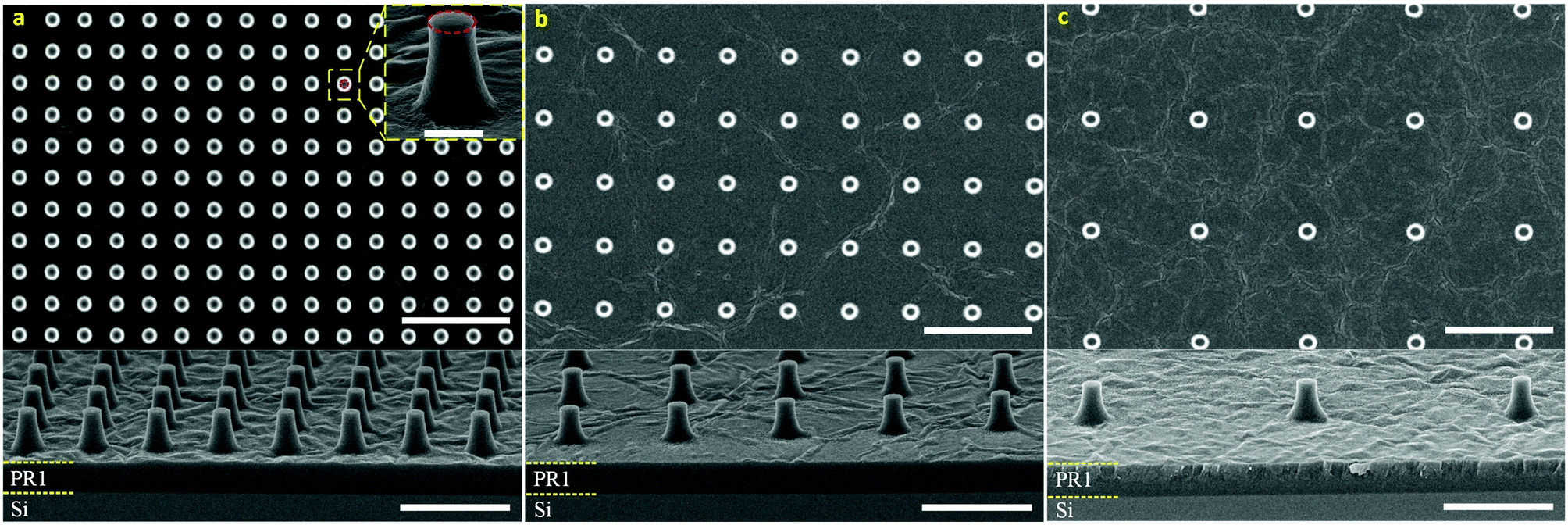 | ||
| Fig. 2 Top-view (scale bar: 10 μm) and cross-sectional (scale bar: 5 μm) HR-SEM images of sub-μm PR column arrays with different pitches of (a) 3 μm, (b) 5 μm, and (c) 10 μm, fabricated on top of PR1. The black spots and the white rings in the top-view images indicate the flat-top and the sidewall slope of the PR columns, respectively. The close-up image (scale bar: 1 μm) in (a) shows the shape of a fabricated PR column, which has a sub-μm flat-top indicated by a red circle, and a sloped sidewall profile. | ||
Spin-coating of PDMS![[thin space (1/6-em)]](https://www.rsc.org/images/entities/h3_char_2009.gif) :hexane solution over sub-μm photoresist column arrays
:hexane solution over sub-μm photoresist column arrays
Fig. 3 shows the cross-sectional HR-SEM images of sub-μm PR column arrays, spin-coated with the PDMS:hexane (1:10) solution, followed by baking at 80 °C for 3 h. At a high spinning speed of 6000 rpm for 3 min, the PDMS:hexane solution was uniformly spread over the surface, and it homogenously covered all the PR columns. It is worth mentioning that the thickness of the PDMS layer after curing was much smaller than the height of the fabricated PR columns, i.e. 1.35 ± 0.02 μm versus 1.71 ± 0.04 μm, respectively. However, a thin PDMS layer was found to cover the flat-top of the PR columns. The red arrow in Fig. 3a indicates the unexpected breaking of this thin film caused by the breaking of the sample for SEM observation. The coverage of such a PDMS thin film over the top of the microcolumns when spin-coating PDMS solution over the microcolumn arrays is a typical problem reported in the literature.34,35 It can be attributed to the flexibility of PDMS, leading to the ductility of the PDMS thin films. The cross-sectional views of the holes in the PDMS membranes, Fig. 3a and b, show truncated cone-shaped holes, which were replicated from the periodic sub-μm PR columns as master molds. The difference in the size of the holes observed in Fig. 3a and b and the deformation of the membrane surface observed in Fig. 3c probably came from the stretching of the membranes when breaking the sample for SEM observation. In addition, a low surface roughness (Ra = 0.45 nm over an area of 1 × 1 μm2) of the PDMS membranes measured using an AFM indicated a smooth membrane surface after the spin-coating and curing processes (Fig. S2†).
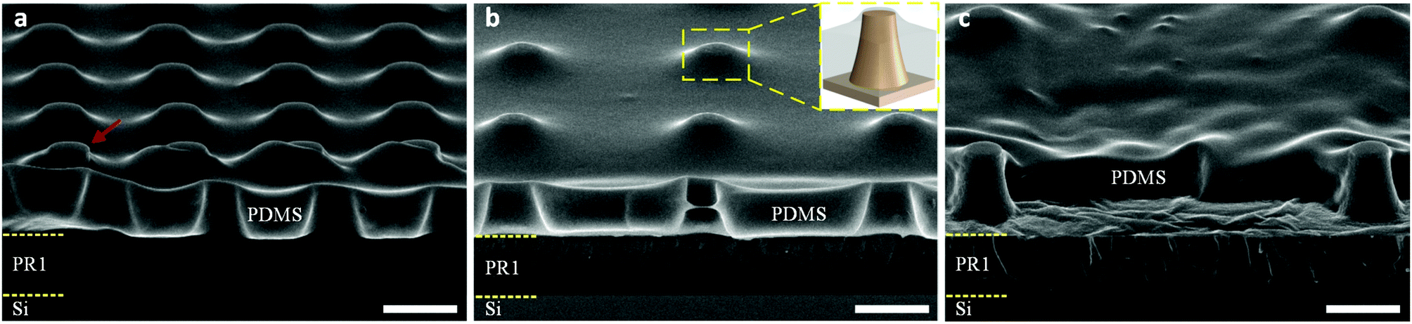 | ||
| Fig. 3 Cross-sectional HR-SEM images of PR column arrays with different pitches of (a) 3 μm, (b) 5 μm, and (c) 10 μm, coated with the cured PDMS:hexane (1:10) solution. The red arrow in (a) indicates the breaking of the PDMS thin film covered on the flat-top of the PR columns – inserted image in (b) – which was caused by breaking the sample for SEM observation. Scale bars represent 2 μm. | ||
Through-hole opening using reactive plasma etching of PDMS
Fig. 4 shows the cross-sectional HR-SEM images of sub-μm PR column arrays coated with PDMS, which were etched at various etching times in the reactive ion etching system (in-house built TEtske system). From the observation, a uniform etching of the PDMS layer was obtained for all arrays. Upon etching the thin PDMS film covered on the flat-top of the PR columns, the holes were opened after an etching time of 15 s. By increasing the etching time, membranes with a thickness of 600 ± 20 nm were obtained after an etching time of 60 s. At a thickness less than 1 μm, the effective Young's modulus of PDMS has been reported to significantly increase to approximately 8 MPa, which is ten times higher than that of a PDMS layer of 0.5 mm thickness.36 This effective Young's modulus of a sub-μm PDMS is comparable to that of a tissue culture plastic (TCP) substrate, i.e. ∼10 MPa.37 The average thicknesses of the PDMS through-hole membranes at various etching times are presented in Table 1. It is clearly observed that the standard deviation calculated from the measured thickness values of the membranes was relatively large. We attribute this mainly to the errors in the thickness measurement of the exact values due to the stretching of the membranes caused by the breaking of samples for cross-sectional SEM measurement (Fig. S3†).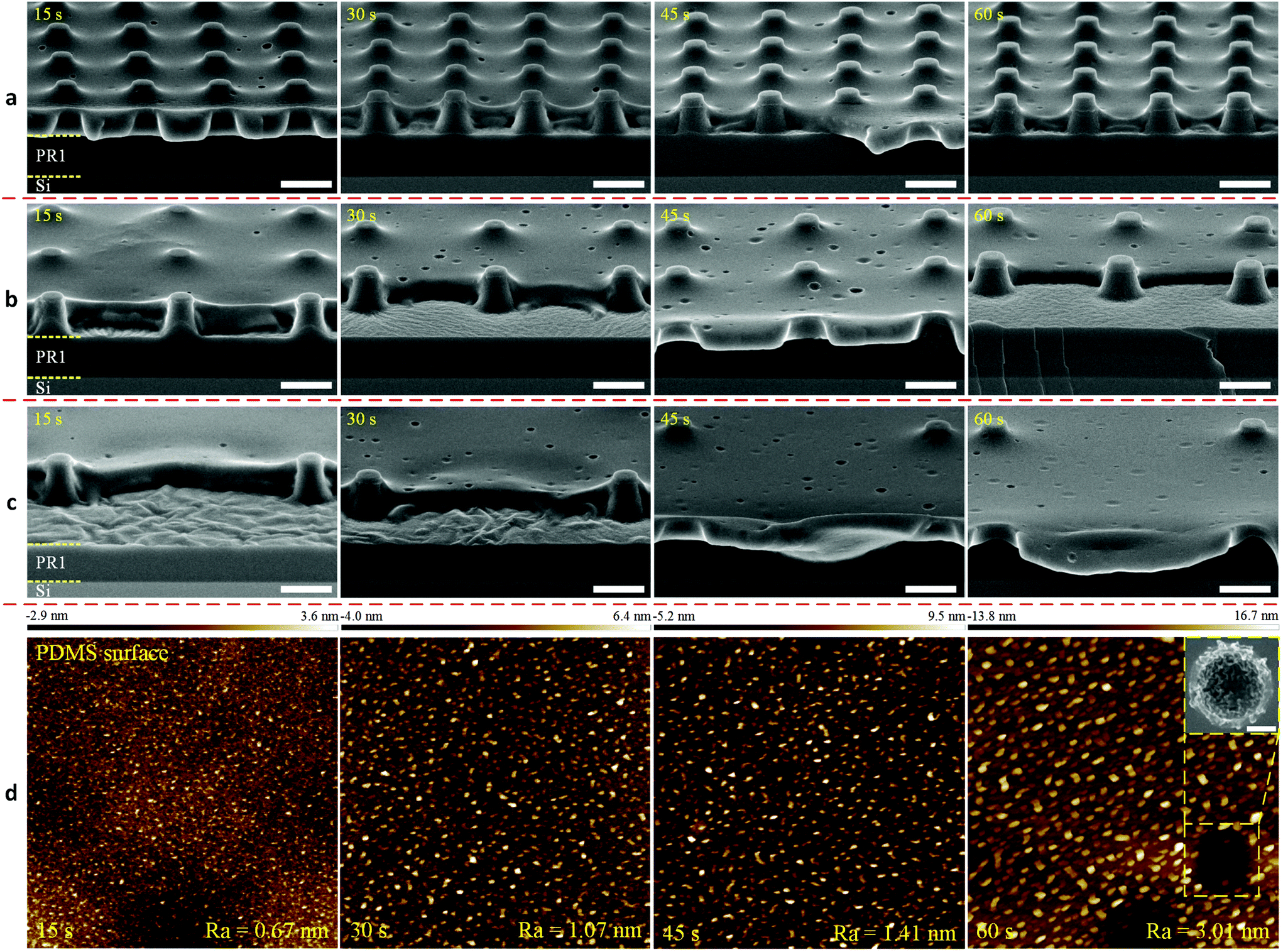 | ||
| Fig. 4 Cross-sectional HR-SEM images of PDMS-coated PR column arrays with different pitches of (a) 3 μm, (b) 5 μm, and (c) 10 μm, etched at various etching times. Scale bars represent 2 μm. (d) AFM images (scan field: 1 × 1 μm2) of the PDMS membrane surface with the measured roughness (Ra) at various etching times. The inserted HR-SEM image in (d) shows a close-up image (scale bar: 200 nm) of a hole on the surface of the PDMS membrane observed after the etching process. | ||
| Etching time (s) | Membrane thickness (nm) | Standard deviation (nm) |
|---|---|---|
| 0 | 1345 | 20 |
| 15 | 1170 | 26 |
| 30 | 940 | 20 |
| 45 | 749 | 23 |
| 60 | 600 | 20 |
Fig. 4d shows the average surface roughness (Ra) of a PDMS membrane at various etching times, which was measured over an area of 1 × 1 μm2 (Fig. S4†). A slight increase in the surface roughness from 0.67 nm to 3.01 nm was observed with an increase in the etching time from 15 s to 60 s, respectively. This is a typical problem encountered with plasma etching, which is based on the physical bombardment of high energy particles.32 The close-up HR-SEM image in Fig. 4d shows a nanohole on the surface of the PDMS membrane, which was observed only after the etching process. From the observations made in Fig. 4a and c, the number of these nanoholes did not increase with the increase in the etching time (Fig. S5†). Therefore, we attribute these nanoholes to nanobubbles trapped inside the PDMS membranes. These nanobubbles were probably created during the spin-coating of this solution over the fabricated PR arrays at a high speed of 6000 rpm. By etching the top layer of the membrane, these nanoholes became exposed to the membrane surface. In addition, after etching for 60 s, sulfur (S) residues were found on the PDMS membrane surface by using energy dispersive X-ray spectrometry (EDS), though at a relatively low percentage of approximately 1.5 wt% (Fig. S6†). Fig. 5 and Table 1 show the etching rate of the cured PDMS:hexane versus the etching time. From the linear fit curve, the etching rate of the cured PDMS:hexane (1:10) solution could be determined as 740 nm min−1. The inserted HR-SEM images in Fig. 5 show that the curvature of the PDMS layer around the PR columns increased with the increasing etching time. Moreover, the opening of the through-holes also increased with the decrease in the membrane thickness due to the sidewall slope profile of the fabricated PR columns.
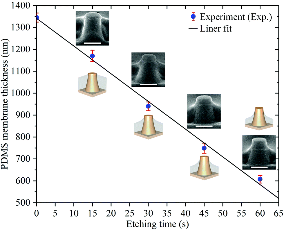 | ||
| Fig. 5 Etching rate of the cured PDMS:hexane as a function of the etching time. The inserted sketches and HR-SEM images (scale bar: 1 μm) show the geometry of the structures etched at various etching times. | ||
Releasing of the sub-μm PDMS through-hole membranes
Fig. 6 shows the top-view optical and HR-SEM images of a free-standing and sub-μm PDMS membranes with through-holes of 810 ± 20 nm in diameter, with different hole interspacings of 3 μm, 5 μm, 10 μm. No cracking or breaking of the large-area membranes was observed upon releasing them with the 3D-printed ring from the positive PR structures in acetone, thus indicating that this procedure enables a smooth detachment (Fig. S7†). It is worth mentioning that the free-standing membranes (3 cm in diameter) were vibrating continuously during the observation using the optical microscope (Movie S1†), probably due to air convection. This led to a significant change in the observed color of the light transmitted through the through-holes, which are indicated by red circles in the close-up optical image. The black holes in the HR-SEM images again indicate a through-hole membrane.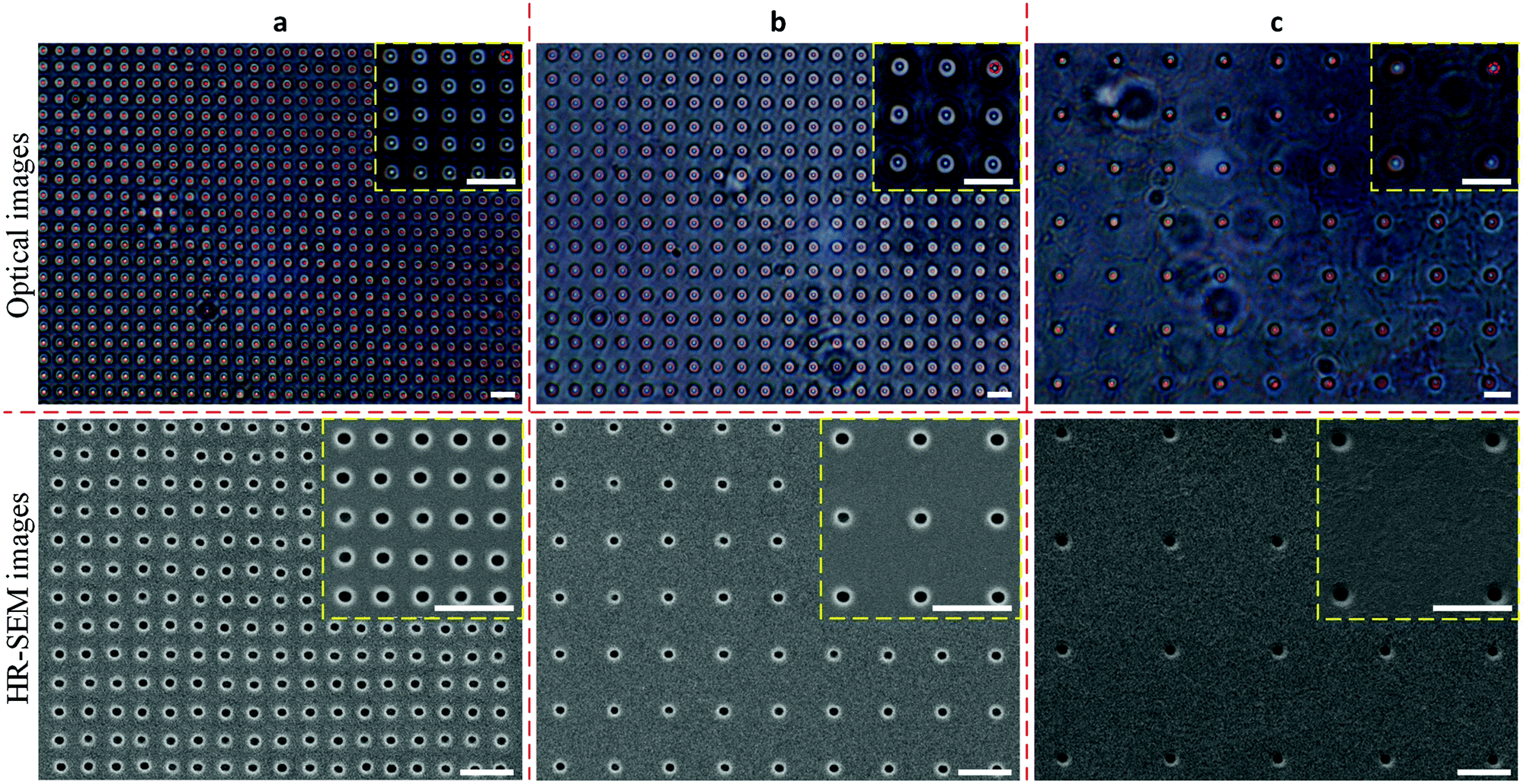 | ||
| Fig. 6 Top-view optical (top) and HR-SEM (bottom) images of the free-standing and sub-μm PDMS through-hole membranes with different hole interspacings of (a) 3 μm, (b) 5 μm, and (c) 10 μm. Scale bars represent 5 μm. | ||
Cell viability and morphology after culture on the PDMS through-hole membranes
After successful release of the sub-μm PDMS through-hole membranes and mounting of the membranes on a support ring to create a Transwell-like culture set-up (Fig. S8†), the Transwell was fully immersed in 70% ethanol for 2 h, and subsequently in PBS solution for 1 h. After this sterilization process, the cells were added on top of the membrane and allowed to adhere and proliferate. Fig. 7a shows the top-view fluorescent images of the cells on the membrane after a live/dead staining. It can be observed that most of the cells (∼94%) were viable (green) after 7 days (Fig. S9 and S10†). The number of dead cells (red) (∼6%) were relatively low and comparable to that of the same cells cultured on a Transwell permeable support (Corning Inc., USA), i.e. ∼8% (Fig. S11†). From this result it can be concluded that the membranes do not induce any acute cytotoxic response. In Fig. 7b, the cell morphology was observed to be normal with most cells showing an endothelial-like bipolar spread morphology. There were no abnormalities found in the morphology of the cell nuclei. A similar cell morphology was observed when these cells were cultured on a TCP substrate (Fig. S12†). Therefore, this membrane can be considered as a cell culture substrate in studies where, for example, the role of direct-cell contacts or paracrine signaling between compartmentalized co-cultures is of interest. The membrane would in this case be a model of the basal lamina and allow for both sprouting of cells’ filopodia through the through-holes and the fast diffusion of soluble factors from one compartment to the other by passing through the sub-μm length of the through-holes. | ||
| Fig. 7 Top-view fluorescent images of cultured cells on sub-μm PDMS through-hole membranes. (a) Live/dead staining combined with nuclei staining (NucBlue™) after 7 days shows a relatively high number (∼94%) of viable cells (green) with a relatively low number of dead cells (red). (b) This merged image of the PDMS membrane (grayscale after bright field imaging) and an ActinGreen™ and NucBlue™ staining, shows the spread morphology of the cells on the membrane. Scale bars represent (a) 400 μm and (b) 50 μm. | ||
Conclusions
In summary, we report and demonstrate a robust and simple method for fabricating free-standing and sub-μm PDMS through-hole membranes over large areas, combining soft lithography with reaction plasma etching techniques. Using this method, we fabricated free-standing PDMS membranes with various sub-μm thicknesses over areas as large as 3 cm in diameter, possessing periodic sub-μm through-holes of 810 ± 20 nm in diameter with different hole interspacings of 3 μm, 5 μm, and 10 μm. Through its simple procedure, our fabrication method provides an enabling technique for large-scale and rapid patterning of sub-μm PDMS through-hole membranes, which is suitable for high-yield production at low cost.Furthermore, we demonstrated the use of our fabricated PDMS membranes as a cell culture substrate for biomedical applications by culturing endothelial cells on the membranes in a Transwell-like set-up. Future work with this setup will allow us to further characterize the mechanical properties, permeability and transport selectivity of the membrane.36 In addition, the effect of our membrane on the co-cultures of multiple cell types on the opposite sides of the membrane can be investigated.38
Our research into the integration of these fabricated PDMS through-hole membranes into microfluidic chips is also ongoing. For example, we wish to use these membranes as part of the blood–brain barrier-on-a-chip as shown in the ESI (Fig. S13†).39 In this device, the quality of the cultured cell layer and its response to mechanical cues can be easily studied by measuring the trans endothelial electrical resistance (TEER).7
Conflicts of interest
There are no conflicts to declare.Acknowledgements
This work was supported by the Netherlands Center for Multiscale Catalytic Energy Conversion (MCEC), and the Netherlands Organisation for Scientific Research (NWO) Gravitation programme funded by the Ministry of Education, Culture and Science of the government of the Netherlands. Additionally, it was funded by the ERC Advanced Grant (Vescel) of Prof. Dr Ir Albert van den Berg.References
- T. A. Desai, D. J. Hansford, L. Kulinsky, A. H. Nashat, G. Rasi, J. Tu, Y. Wang, M. Zhang and M. Ferrari, Biomed. Microdevices, 1999, 2, 11–40 CrossRef CAS.
- S. P. Adiga, C. Jin, L. A. Curtiss, N. A. Monteiro-Riviere and R. J. Narayan, Wiley Interdiscip. Rev.: Nanomed. Nanobiotechnol., 2013, 1, 568 CrossRef PubMed.
- M. M. Pérez-Madrigal, M. I. Giannotti, L. J. Del Valle, L. Franco, E. Armelin, J. Puiggalí, F. Sanz and C. Alemán, ACS Appl. Mater. Interfaces, 2014, 6, 9719–9732 Search PubMed.
- J. A. Rogers and J. H. Ahn, Silicon Nanomembranes: Fundamental Science and Applications, Wiley-VCH Verlag GmbH & Co. KGaA, 1st edn, 2016, ch. 1 Search PubMed.
- H. J. Kim, D. Huh, G. Hamilton and D. E. Ingber, Lab Chip, 2012, 12, 2165 RSC.
- D. Huh, H. J. Kim, J. P. Fraser, D. E. Shea, M. Khan, A. Bahinski, G. a Hamilton and D. E. Ingber, Nat. Protoc., 2013, 8, 2135–2157 CrossRef CAS PubMed.
- M. W. van der Helm, M. Odijk, J. P. Frimat, A. D. van der Meer, J. C. T. Eijkel, A. van den Berg and L. I. Segerink, Biosens. Bioelectron., 2016, 85, 924–929 CrossRef CAS PubMed.
- H. D. Tong, H. V. Jansen, V. J. Gadgil, C. G. Bostan, E. Berenschot, C. J. M. Van Rijn and M. Elwenspoek, Nano Lett., 2004, 4, 283–287 CrossRef CAS.
- C. C. Striemer, T. R. Gaborski, J. L. McGrath and P. M. Fauchet, Nature, 2007, 445, 749–753 CrossRef CAS PubMed.
- S. R. Khetani and S. N. Bhatia, Nat. Biotechnol., 2007, 26, 120–126 CrossRef PubMed.
- B. Yuan, Y. Li, D. Wang, Y. Xie, Y. Liu, L. Cui, F. Tu, H. Li, H. Ji, W. Zhang and X. Jiang, Adv. Funct. Mater., 2010, 20, 3715–3720 CrossRef CAS.
- D. Huh, B. D. Matthews, A. Mammoto, M. Montoya-Zavala, H. Y. Hsin and D. E. Ingber, Science, 2010, 328, 1662–1668 CrossRef CAS PubMed.
- T. Masters, W. Engl, Z. L. Weng, B. Arasi, N. Gauthier and V. Viasnoff, PLoS One, 2012, 7, e44261 CAS.
- M. Neklyudova, A. K. Erdamar, L. Vicarelli, S. J. Heerema, T. Rehfeldt, G. Pandraud, Z. Kolahdouz, C. Dekker and H. W. Zandbergen, Appl. Phys. Lett., 2017, 111, 063105 CrossRef.
- J. H. Seo, J. Park, D. Zhao, H. Yang, W. Zhou, B. K. Ju and Z. Ma, IEEE Photonics J., 2013, 5, 2200106 CrossRef.
- J. Li, D. Stein, C. McMullan, D. Branton, M. J. Aziz and J. A. Golovchenko, Nature, 2001, 412, 166–169 CrossRef CAS PubMed.
- B. Mosadegh, M. Agarwal, Y. Torisawa and S. Takayama, Lab Chip, 2010, 10, 1983–1986 RSC.
- W. Chen, N. Huang, K. Kurabayashi and J. Fu, Mtas, 2012, 1849–1851 Search PubMed.
- H. Wei, B. Chueh, H. Wu, E. W. Hall, C. Li, R. Schirhagl, J.-M. Lin and R. N. Zare, Lab Chip, 2011, 11, 238–245 RSC.
- S. K. Sia and G. M. Whitesides, Electrophoresis, 2003, 24, 3563–3576 CrossRef CAS PubMed.
- T. Yanagishita, K. Nishio and H. Masuda, J. Vac. Sci. Technol., B: Microelectron. Nanometer Struct.–Process., Meas., Phenom., 2007, 25, L35 CrossRef CAS.
- S. H. Yun, L. M. Cabrera, J. W. Song, N. Futai, Y. C. Tung, G. D. Smith and S. Takayama, Anal. Chem., 2007, 79, 1126–1134 CrossRef PubMed.
- Y. Luo and R. N. Zare, Lab Chip, 2008, 8, 1688 RSC.
- B. H. Jo, L. M. Van Lerberghe, K. M. Motsegood and D. J. Beebe, J. Microelectromech. Syst., 2000, 9, 76–81 CrossRef CAS.
- H. Cho, J. Kim, H. Park, J. Won Bang, M. Seop Hyun, Y. Bae, L. Ha, D. Yoon Kim, S. Min Kang, T. Jung Park, S. Seo, M. Choi and K.-Y. Suh, Nat. Commun., 2014, 5, 3137 Search PubMed.
- D. Tahk, S.-M. Paik, J. Lim, S. Bang, S. Oh, H. Ryu and N. L. Jeon, Lab Chip, 2017, 17, 1817–1825 RSC.
- E. Kang, J. Ryoo, G. S. Jeong, Y. Y. Choi, S. M. Jeong, J. Ju, S. Chung, S. Takayama and S. H. Lee, Adv. Mater., 2013, 25, 2167–2173 CrossRef CAS PubMed.
- H. Le-The, E. Berenschot, R. M. Tiggelaar, N. R. Tas, A. van den Berg and J. C. T. Eijkel, Microsyst. Nanoeng., 2018, 1–11 Search PubMed.
- R. H. Collins and F. T. Deverse, US3549368, 1970 Search PubMed.
- H. Le-The, E. Berenschot, R. M. Tiggelaar, N. R. Tas, A. van den Berg and J. C. T. Eijkel, Adv. Mater. Technol., 2017, 2, 1600238 CrossRef.
- J. Garra, T. Long, J. Currie, T. Schneider, R. White and M. Paranjape, J. Vac. Sci. Technol., A, 2002, 20, 975–982 CAS.
- M. J. Madou, Fundamentals of Microfabrication and Nanotechnology, CRC press, Boca Raton, 2nd edn, 2002 Search PubMed.
- J. Schindelin, I. Arganda-Carreras, E. Frise, V. Kaynig, M. Longair, T. Pietzsch, S. Preibisch, C. Rueden, S. Saalfeld, B. Schmid, J. Y. Tinevez, D. J. White, V. Hartenstein, K. Eliceiri, P. Tomancak and A. Cardona, Nat. Methods, 2012, 9, 676–682 CrossRef CAS PubMed.
- K. Atsuta, H. Noji and S. Takeuchi, Lab Chip, 2004, 4, 333–336 RSC.
- J. H. Kang, E. Um and J.-K. Park, J. Micromech. Microeng., 2009, 19, 45027 CrossRef.
- J. Gao, D. Guo, S. Santhanam and G. K. Fedder, J. Microelectromech. Syst., 2015, 24, 2170–2177 CrossRef CAS.
- D. E. Discher, Science, 2005, 310, 1139–1143 CrossRef CAS PubMed.
- I. D. Huh, B. Matthews, A. Mammoto, M. Montoya-Zavala and H. Hsin, Science, 2010, 328, 1662–1668 CrossRef PubMed.
- M. W. Van Der Helm, A. D. Van Der Meer, J. C. T. Eijkel, A. van den Berg and L. I. Segerink, Tissue Barriers, 2016, 8370, 1–13 Search PubMed.
Footnote |
| † Electronic supplementary information (ESI) available. See DOI: 10.1039/c7nr09658e |
| This journal is © The Royal Society of Chemistry 2018 |