Towards substrate engineering of graphene–silicon Schottky diode photodetectors†
Abstract
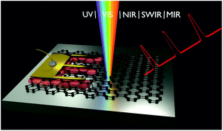
Graphene–silicon Schottky diode photodetectors possess beneficial properties such as high responsivities and detectivities, broad spectral wavelength operation and high operating speeds. Various routes and architectures have been employed in the past to fabricate devices. Devices are commonly based on the removal of the silicon-oxide layer on the surface of silicon by wet-etching before deposition of graphene on top of silicon to form the graphene–silicon Schottky junction. In this work, we systematically investigate the influence of the interfacial oxide layer, the fabrication technique employed and the silicon substrate on the light detection capabilities of graphene–silicon Schottky diode photodetectors. The properties of devices are investigated over a broad wavelength range from near-UV to short-/mid-infrared radiation, radiation intensities covering over five orders of magnitude as well as the suitability of devices for high speed operation. Results show that the interfacial layer, depending on the required application, is in fact beneficial to enhance the photodetection properties of such devices. Further, we demonstrate the influence of the silicon substrate on the spectral response and operating speed. Fabricated devices operate over a broad spectral wavelength range from the near-UV to the short-/mid-infrared (thermal) wavelength regime, exhibit high photovoltage responses approaching 106 V W−1 and short rise- and fall-times of tens of nanoseconds.


 Please wait while we load your content...