
 Open Access Article
 This Open Access Article is licensed under a
 Creative Commons Attribution 3.0 Unported Licence
Insights into the formation mechanism of two-dimensional lead halide nanostructures†
Eugen
Klein
a,
Rostyslav
Lesyuk
ab and
Christian
Klinke
 *ac
*ac
aInstitute of Physical Chemistry, University of Hamburg, Grindelallee 117, 20146 Hamburg, Germany. E-mail: klinke@chemie.uni-hamburg.de
bPidstryhach Institute for applied problems of mechanics and mathematics of NAS of Ukraine, Naukowa str. 3b, 79060 Lviv, Ukraine
cDepartment of Chemistry, Swansea University – Singleton Park, Swansea SA2 8PP, UK
First published on 9th February 2018
Abstract
We present a colloidal synthesis strategy for lead halide nanosheets with a thickness of far below 100 nm. Due to the layered structure and the synthesis parameters the crystals of PbI2 are initially composed of many polytypes. We propose a mechanism which gives insight into the chemical process of the PbI2 formation. Further, we found that the crystal structure changes with increasing reaction temperature or by performing the synthesis for longer time periods changing for the final 2H structure. In addition, we demonstrate a route to prepare nanosheets of lead bromide as well as lead chloride in a similar way. Lead halides can be used as a detector material for high-energy photons including gamma and X-rays.
1. Introduction
Two-dimensional nanostructures represent an important field in colloidal syntheses with a wide range of applications.1–3 Iron sulfide (Fe3S4) nanosheets (NS) for example, are used as anode materials for lithium-ion batteries.4 Cadmium selenide (CdSe) is one of the best-known semiconductor materials and finds application in many fields of research like in photocatalysis or in optoelectronics.5,6 Further, various other two-dimensional semiconductor nanocrystals are suited as materials in transistor devices due to the high conductivity in plane.7–9 An important scientific field is represented by materials like gallium nitride (GaN) or gallium oxide (Ga2O3) which are used as UV photodetectors due to their large band gap.10,11 Compared to thin films composed of small nanoparticles, 2D nanostructures have the advantage that they do not exhibit tunnel barriers or grain boundaries in the lateral dimensions, which makes them interesting for optoelectronics, photovoltaics,12,13 in particular for flexible electronic devices.14There are many ways to synthesize 2D nanostructures like exfoliation of layered structures, solvothermal methods, chemical vapor deposition, and direct colloidal synthesis in a flask. Chemical exfoliation based techniques use either neutral or charged molecules or ions in order to separate the layered structures through intercalation, yielding single- or multilayer nanosheets.15–17 Solvothermal methods are performed in a stainless steel autoclave in water (hydrothermal) or other polar solvents like ethylene glycol at high pressure.18,19 Thin sheets prepared by chemical vapor deposition grow on a substrate which is placed in a closed reaction chamber that is filled with one or more volatile precursors. By using this technique it is possible to produce high quality solid materials like GeSe, MoSe2 or WSe2.20–22 The synthesis in a flask can be executed through a single source precursor,23 by adding one of the reaction partners with a syringe pump over a certain time period,24 or by using the hot injection method where the second reactant is rapidly introduced to the reaction mixture.25 An important advantage of the methods following the colloidal route is low-cost solution processability.
In order to obtain nanostructures with specific shapes like 0D spheres, 1D wires or 2D sheets, ligands which passivate energetically favorable facets are the most important factor. Metal-free ligands such as chalcogenides and hydrochalcogenides (S2−, HS−, Se2−, HSe−, Te2−, HTe−, TeS32−)26 or metal-containing ligands like a tungsten arsenate oxide27 are used in various synthesis of nanomaterials, however the most prominent ligands are organic compounds like oleic acid, oleylamine or trioctylphosphine (TOP).28,29 Additionally, co-ligands namely halogen alkanes can be used to synthesize CdSe pyramids or PbS nanosheets.13,30
Lead iodide is a direct band gap semiconductor with a gap between 2.3 and 2.4 eV (ref. 31) and a crystal structure which consist of layers of hexagonally close packed iodine and lead atoms oriented perpendicular to the c-axis.32–34 Using specific synthesis parameters it is possible to prepare crystals of PbI2 with specific orientations of the layers. These specific orientations of layers are called polytypes. The most frequent polytype is the 2H lead iodide34 having the stacking sequence (AαB), where A, B denote iodine ions, and α the lead ion.
The potential applications for this material are high energy photon detectors for X-rays and gamma rays and photocells.32 PbBr2 and PbCl2 are wide band gap materials with an orthorhombic crystal structure. All three lead halides find application as precursor materials in the perovskite solar cell fabrication.35
Here, we report on the synthesis and characterization of PbI2, PbBr2 and PbCl2 nanosheets prepared via a direct colloidal route. The nanosheets are analyzed by NMR, TEM, XRD, AFM and UV/Vis techniques. To our best knowledge we report for the first time syntheses of two-dimensional PbBr2, PbCl2 and PbI2 sheets with thicknesses far below 100 nm. In addition to the possible formation process, we also provide insights into the thermodynamically triggered change of the crystal structure.
2. Experimental section
Synthesis
All chemicals were used as received: lead(II) acetate tri-hydrate (Aldrich, 99.999%), oleic acid (OA, Aldrich, 90%), 1-chlorotetradecane (CTD; Aldrich, 98%), 1-bromotetradecane (BTD; Aldrich, 97%), tri-octylphosphine (TOP; ABCR, 97%), and 1,2-diiodoethane (DIE; Aldrich, 99%).Investigation on the reaction mechanism: to ensure the presence of the 1,2-diiodoethane peak in the 1H NMR the synthesis for the PbI2 nanosheets was performed at higher concentrations. 564 mg of 1,2-diiodoethane (2 mmol) were dissolved in 4 mL of oleic acid and 2.66 mL of this precursor were added to the reaction mixture described above.
NMR
Nuclear magnetic resonance measurements were performed on a Bruker AVANCE 400 MHz Spectrometer (AV4002) for 1H NMR and a Bruker DRX 500 MHz Spectrometer (AV500) for 31P NMR.TEM
The TEM samples were prepared by diluting the nanosheet suspension with toluene followed by drop casting 10 μL of the suspension on a TEM copper grid coated with a carbon film. Standard images were done on a JEOL-1011 with a thermal emitter operated at an acceleration voltage of 100 kV.XRD
X-ray diffraction measurements were performed on a Philips X'Pert System with a Bragg–Brentano geometry and a copper anode with a X-ray wavelength of 0.154 nm. The samples were measured by drop-casting the suspended nanosheets on a <911> or <711> cut silicon substrate.AFM
Atomic force microscopy measurements were performed in tapping mode on a Veeco MultiMode NanoScope 3A and a JPK Nano Wizard 3 AFM in contact mode. The samples were prepared by drop-casting a diluted nanosheet suspension on a silicon wafer.Spectroscopy
UV/vis absorption spectra were obtained with a Cary 5000 spectrophotometer equipped with an integration-sphere. The PL spectra measurements were obtained by a fluorescence spectrometer (Fluoromax-4, Horiba Jobin Yvon).3. Results and discussion
Chemical reaction
Controlling the size and shape of nanocrystals requires the knowledge of the function and purpose of every reactant which participates in the reaction. Therefore a fundamental investigation and understanding of the mechanism is crucial. The two-dimensional PbI2 NS are produced by injecting a DIE oleic acid solution and TOP separately into a degassed lead oleate oleic acid mixture preheated to 80 °C. In order to verify the exact function of TOP and any other reactions in the synthesis several aliquots taken during the reaction were investigated by 1H and 31P NMR spectroscopy. Fig. 1A shows the 1H NMR spectrum of aliquots taken from one and the same synthesis at different times. All of the peaks in the spectra belong to oleic acid except the one at 2.67 ppm and nearly all of them show no shift as a function of changes in the environment like pH or volume. The peak at 2.67 ppm can be assigned to 1,2-diiodoethane with a singlet due to the equivalence of the protons (Fig. 1B). The only peak that is shifting is the proton of the carboxylic group between 12.25 ppm and 12.32 ppm shown in Fig. 1C. Further, 31P NMR was performed for the last step in which TOP was added. Fig. 1D shows that even right after the injection all of the TOP molecules have already reacted and only tri-octylphosphine oxide (TOPO) can be observed. The TOPO shift appears at slightly higher values due to a change in the local environment with the formation of PbI2 nanoparticles.36 Based on these results we propose a mechanism depicted in Scheme 1 for the synthesis of PbI2 nanoparticles which takes place in two steps. The first step starts after the injection of 1,2-diiodoethane which reacts with oleic acid resulting in the substitution of one of the iodide ions. The free iodide ion and the proton of the coordinated oleic acid forms hydroiodic acid and thereby decreases the pH-level of the solution. This change can be followed by the shift of the peak of the carboxylic group from 12.25 ppm to 12.27 ppm. At last the hydroiodic acid reacts with the lead oleate to form PbI2 monomers and oleic acid. Since the time duration between the first and second aliquot was 4 min but the shift of the peak was small as well as no color change could be observed in the reaction mixture we believe that this first step happens very slowly. Syntheses without TOP at 200 °C and above lead to PbI2 sheets. Therefore, TOP is not needed for the reaction to take place (Fig. S1A†). A more direct approach to prepare PbI2 nanosheets were syntheses with potassium iodide (KI) and ammonium iodide (NH4I). Particles prepared by following these procedures could only be obtained at temperatures of 150 °C and above and showed thicknesses similar to the NS synthesized without TOP which were thicker than 50 nm. | ||
| Fig. 1 1H and 31P NMR spectra of aliquots taken from one synthesis over time. (A) 1H NMR spectra of four aliquots with all their corresponding peaks. (B) Region of 1,2-diiodoethane peak. (C) Region of the carboxylic group peak and its shifting. (D) 31P NMR for the aliquots taken after the injection of TOP. | ||
 | ||
| Scheme 1 Proposed mechanism for the synthesis of PbI2 nanosheets in two steps. (A) describes the slow reaction where TOP is not involved. (B) shows the synthesis after the injection of TOP. | ||
The second step starts with the injection of TOP which substitutes an iodide atom at the 1,2-diiodoethane and resulting in the release of an iodide ion. This reacts again to hydroiodic acid and further with lead oleate to a lead oleate iodide complex which can be observed by the shift of the carboxylic group from 12.27 ppm to 12.31 ppm. Finally the lead oleate iodide complex can react in the way proposed in Scheme 1B following step 1 or step 2 to form PbI2 monomers and a TOP oleate molecule. This phosphorous molecule forms an anhydrate and TOPO that can be detected in the 31P NMR.36 Due to the relatively strong shift from 12.27 ppm to 12.31 ppm right after the injection of TOP we believe that a large amount of hydroiodic acid is produced and therefore the second step occurs much faster than the first one. Further indications are provided by the 31P NMR taken after the TOP injection. The spectrum shows only the peak for TOPO and that the reaction mixture turns from clear colorless to a turbid yellow-green solution. This means that all TOP molecules react instantly with 1,2-diiodoethane, producing a large amount of PbI2 monomers. This process leads to a much faster supersaturation of the mixture and therefore an increase of the reactivity in this system. The last aliquot shows a shift of the carboxylic proton from 12.31 ppm to 12.29 ppm. 4 min after the injection of TOP most of the hydroiodic acid produced at the beginning of the second step was used up and the pH has increased. The fact that the peak for the 1,2-diiodoethane appears in the last 1H NMR spectrum means the reaction is not finished. The reaction parameters were selected to produce sheets with the smallest thickness. Therefore, an amount of lead and iodide precursors was chosen which could not completely react within the given time period. Many authors have reported about the effect of phosphines and phosphine impurities to reduce lead oleate to Pb0 species.36–38 In our case the formation of Pb0 can be excluded due to several reasons. Literature reports describe reactions at temperatures above 140 °C (and some state that) with a large amount of TOP (5 mL) and reaction times of hours are needed to generate Pb0. In contrast to them, our reaction temperature lies at 80 °C and the amount of TOP is very limited (0.06 mL) for the described mechanism. Moreover there is no chemical in our approach which could oxidize Pb0 back to the Pb2+ species.
Change of the space group
Fig. 2 shows representative TEM images for PbI2 nanosheets prepared by varying the growth time between 0 min and 60 min with all other reaction parameters remaining constant. All four samples consist of nanosheets with a hexagonal shape while exhibiting a strong tendency to stack. The dimensions of these particles are more or less the same having lateral sizes between 1.5 μm and 4 μm. On the basis of the data shown in Fig. 2 the sheets have a homogeneous surface and well defined edges. Fig. S1B† presents an overview for particles prepared immediately after the formation. The thickness was calculated by measuring the width of the reflex at 39° in the powder X-ray diffractograms (Fig. 3). This reflex represents the <001> direction in our XRD measurements on the substrate. By using a Gauss fit for the reflex at 39° the full width at half maximum (FWHM) changes only slightly with longer growth periods. The calculated thicknesses from the FWHM values using the Scherrer equation39 (with a form factor of 1) were 21.3 nm (0 min), 18.7 nm (5 min), 17.3 nm (20 min), and 27.6 nm (60 min) respectively. The X-ray diffractogram of the sheets prepared immediately after the formation reveal a hexagonal crystal structure with the P3m1 space group (Fig. 3). Most of the theoretically possible reflexes do not appear due to the planar orientation of the sheets on the substrate. The tendency of the sheets to orientate themselves parallel on the substrate can be described as a texture effect where only lattice planes parallel to the substrate can be measured in the possible angle range. Increasing the growth time to 5 min and 20 min gives rise to some additional reflexes at the angles of 12°, 25° and 52° while reducing the intensity of the peaks at 15°, 23°, 46° and 56°. Syntheses stopped after even longer growth times like 1 h show the complete omission of the peaks at 15°, 23°, 46° and 56°. This indicates that the space group of the particles changes from the P3m1 to the more symmetric P![[3 with combining macron]](https://www.rsc.org/images/entities/char_0033_0304.gif) m1 with time. Based on the missing of a large number of reflexes in all the shown XRDs and therefore to ensure the crystal structure, X-ray diffraction in a capillary was performed on the products prepared after 0 min and 60 min (Fig. S2†). For the sheets synthesized after 60 min all of the corresponding reflexes can be observed while the diffractogram for the 0 min sample does not show all of the reflexes for the P3m1 space group. A reason for this is probably the relatively small intensities of the major part of the reflexes of 0.1% taken from the literature which makes them disappear in the noise of the measurement. More important is the fact that the particles prepared after 60 min have only the reflexes of the space group Pm1 thus the missing of these reflexes was not due to the texture effect. In an attempt to assign the right polytype to the sample obtained immediately after the sheets formation, we compared the measured capillary XRD pattern with simulated XRD patterns for 2H, 4H, 6H, 8H, 10H, 14H and 20H structures. For the 4H, 10H and 20H polytypes the crystallographic data are based on references.34,40 For other polytypes higher than 4H we built similar sequences always adding another (AαB) block to the structure. For the 20H the sequence (AαB)(AαB)(AαB)(AαB)(AαB)(AαB)(AαB)(AαB)(CβB)(CβB) was adapted from ref. 40. Our study indicates that the kinetic product of our synthesis after 0 min may contain several polytypes,41,42 including 10H, 20H and the 4H (Fig. S3 and further discussion in the ESI†).
m1 with time. Based on the missing of a large number of reflexes in all the shown XRDs and therefore to ensure the crystal structure, X-ray diffraction in a capillary was performed on the products prepared after 0 min and 60 min (Fig. S2†). For the sheets synthesized after 60 min all of the corresponding reflexes can be observed while the diffractogram for the 0 min sample does not show all of the reflexes for the P3m1 space group. A reason for this is probably the relatively small intensities of the major part of the reflexes of 0.1% taken from the literature which makes them disappear in the noise of the measurement. More important is the fact that the particles prepared after 60 min have only the reflexes of the space group Pm1 thus the missing of these reflexes was not due to the texture effect. In an attempt to assign the right polytype to the sample obtained immediately after the sheets formation, we compared the measured capillary XRD pattern with simulated XRD patterns for 2H, 4H, 6H, 8H, 10H, 14H and 20H structures. For the 4H, 10H and 20H polytypes the crystallographic data are based on references.34,40 For other polytypes higher than 4H we built similar sequences always adding another (AαB) block to the structure. For the 20H the sequence (AαB)(AαB)(AαB)(AαB)(AαB)(AαB)(AαB)(AαB)(CβB)(CβB) was adapted from ref. 40. Our study indicates that the kinetic product of our synthesis after 0 min may contain several polytypes,41,42 including 10H, 20H and the 4H (Fig. S3 and further discussion in the ESI†).
 | ||
| Fig. 2 TEM images of PbI2 nanosheets prepared by varying the growth time. The growth time increases from immediately after formation (A) to 5 min (B) to 20 min (C), and to 1 h (D) respectively. Despite being prepared for different growth periods, the particles exhibit the same sizes in all three directions. PbI2 is easily affected by the electron-beam and therefore the sheets get slowly destroyed in the TEM. The small dots in (C) are decomposed and remerged material from the sheet structure. | ||
 | ||
| Fig. 3 Powder XRD of PbI2 nanosheets prepared with varying the growth period. Particles obtained immediately after the formation of the sheets exhibit signals from the P3m1 space group. By extending the time after the formation the crystal structure shifts to the more symmetric space group of Pm1. | ||
A Schematic illustration of the process occurring during and after the formation of the nanosheets with growth time for the 10H polytype is given in the Fig. 4. At first, the more asymmetric space group P3m1 is formed which has a large lattice parameter (for the (100) plane of 3.4895 nm, for the 20H c = 6.979 nm respectively) and one displaced layer of lead and iodide, respectively. With longer growth periods the displaced planes shift in order to form a more symmetric crystal structure. At this point the reflexes of the space group Pm1 appear while at the same time some reflexes of the P3m1 space group start to disappear. At the end of this process, meaning after one hour growth time the more symmetric space group Pm1 remains to define the two-dimensional crystals. Thus the polytypic transition occurs.
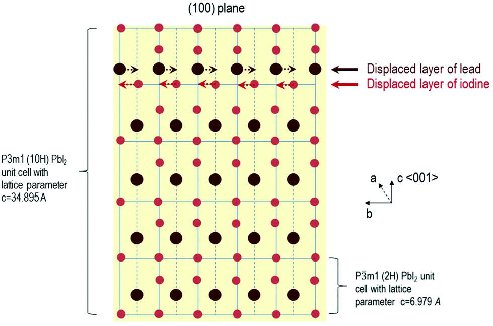 | ||
| Fig. 4 Schematic illustration of the change in space group from P3m1 (shown for the 10H polytype) to Pm1 for PbI2 nanosheets with the growth time. | ||
Comparison with PbBr2 and PbCl2
The PbX2 (X = I, Br, Cl) nanosheet syntheses have a few things in common: the same amount of lead acetate tri-hydrate and TOP. Latter was used in all cases in order to increase the reactivity. For the PbI2 synthesis oleic acid is used in excess and serves as solvent and ligand. The iodide source is 1,2-diiodoethane which is dissolved in oleic acid and must be prepared one to two hours before the injection since it is not long-term stable in solution even when stored in the fridge. TOP is essential for this method due to the fact that the reactivity without it is not high enough and no material would be formed at the given temperatures. The so prepared nanosheets exhibit a uniform size and shape having lateral dimensions of 1.5 μm to 4 μm (Fig. 5A). Nevertheless, the size of the sheets can be controlled between 2 μm and 15 μm by varying the temperature (Fig. S4†). The electron diffraction pattern in Fig. 5B taken from a single sheet shows a dot pattern and indicates that the prepared nanosheets are single crystals. The syntheses of PbBr2 and PbCl2 are carried out in an excess of the corresponding halide sources and at higher temperatures compared to the PbI2 synthesis. By using an excess of long chained haloalkanes like 1-bromotetradecane and 1-chlorotetradecane the reactivity of the reaction can be controlled to a certain degree. Performing the syntheses with haloalkanes possessing shorter alkyl chains like dibromoethene and dichloroethene leads to structures which are several hundred nanometers thick. Higher temperatures of 150 °C and 180 °C are necessary to generate bromine ions and chlorine ions. Fig. 5C shows a TEM image of PbBr2 nanosheets which have a smooth surface and a hexagonal shape. These particles as is the case with PbI2 show a tendency to stack and exhibit a large size distribution between 1 μm and 4 μm. The PbCl2 structures have a stripe- or rod-like shape with lengths between 2 μm to 4 μm and widths between 50 nm to 700 nm (Fig. 5D). As mentioned in the introduction, these materials can be used as precursors for the preparation of the corresponding perovskite structures. Fig. S5† shows TEM images, selected area diffraction pattern (SAED) and XRD of as prepared PbI2 methylammonium iodide particles. They exhibit a hexagon like shape while the single crystal of the PbI2 sheets is somewhat damaged. The reflexes in the XRD fit well with the literature values for the perovskite material.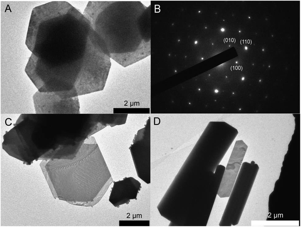 | ||
| Fig. 5 TEM images of PbI2, PbBr2 and PbCl2 nanosheets. (A) PbI2 nanosheets with a hexagon-like morphology and (B) electron diffraction pattern of a single PbI2 nanosheet ([001] zone axis). (C) PbBr2 nanosheets with a high size distribution. (D) Partly 2D PbCl2 nanocrystals. | ||
To discuss the thickness and crystal structure of the fabricated materials powder X-ray diffraction as well as atomic force microscopy measurements were carried out. Fig. S6† shows powder XRDs of PbI2, PbBr2 and PbCl2. PbI2 has a hexagonal crystal structure with a space group of Pm1 while PbBr2 and PbCl2 have an orthorhombic structure with the Pnam space group. The omission of most of the peaks for all three materials can be observed and occurs as a result of the texture effect described earlier. The AFM images and height profiles of PbI2, PbBr2 and PbCl2 are shown in Fig. S7.† The surface of PbI2 NS depicted in Fig. S7A† is not flat compared with PbBr2 nanosheets (Fig. S7B†). The calculated thickness of PbI2 from the XRD data was 21.3 nm and from the AFM measurement 25 nm including the oleic acid shell of 3.6 nm.43 However, the thickness can be varied by many parameters like the temperature, the Pb![[thin space (1/6-em)]](https://www.rsc.org/images/entities/char_2009.gif) :I ratio or nature of the solvent (Fig. S8†). In contrast to PbI2, PbBr2 and PbCl2 show large differences in the values obtained from XRD and AFM. The thicknesses calculated from XRD were 56 nm and 90 nm and from AFM 20 nm and 63 nm for PbBr2 and PbCl2. The larger thicknesses for these two materials are obtained due to the higher reaction temperatures for PbBr2 at 150 °C and PbCl2 at 180 °C compared to PbI2 at 80 °C. The reason for the difference in thickness between AFM and XRD can already be observed in the TEM images for PbBr2 and PbCl2 in Fig. 5 where the darker particles are not solely stacked sheets but also thicker structures. We note that despite the identical crystal structure, the PbBr2 and PbCl2 nanosheets have different shape. PbBr2 tends to form hexagonal structures, the PbCl2 forms elongated 2D structures. The reason behind this peculiarity is the different basal planes of the nanosheets apparently due to different synthesis conditions and unit cell constants. From the XRD and SAED data we conclude that for the PbBr2 the basal plane is the (010) crystallographic plane. In XRD data we observe only the reflexes (020), (040), (060) due to texture effects (Fig. S6A†). The PbCl2 nanosheets crystallize and grow parallel to the (120) plane (we observe the (120), (240) and the (360) reflexes, Fig. S6A†). These data are supported by the SAED patterns (Fig. S6B and C†). This in turn causes different growth directions and shape of the synthesized 2D structures. The shape of the PbI2 structures which have hexagonal symmetry with the basal plane (001) is hexagonal as expected.
:I ratio or nature of the solvent (Fig. S8†). In contrast to PbI2, PbBr2 and PbCl2 show large differences in the values obtained from XRD and AFM. The thicknesses calculated from XRD were 56 nm and 90 nm and from AFM 20 nm and 63 nm for PbBr2 and PbCl2. The larger thicknesses for these two materials are obtained due to the higher reaction temperatures for PbBr2 at 150 °C and PbCl2 at 180 °C compared to PbI2 at 80 °C. The reason for the difference in thickness between AFM and XRD can already be observed in the TEM images for PbBr2 and PbCl2 in Fig. 5 where the darker particles are not solely stacked sheets but also thicker structures. We note that despite the identical crystal structure, the PbBr2 and PbCl2 nanosheets have different shape. PbBr2 tends to form hexagonal structures, the PbCl2 forms elongated 2D structures. The reason behind this peculiarity is the different basal planes of the nanosheets apparently due to different synthesis conditions and unit cell constants. From the XRD and SAED data we conclude that for the PbBr2 the basal plane is the (010) crystallographic plane. In XRD data we observe only the reflexes (020), (040), (060) due to texture effects (Fig. S6A†). The PbCl2 nanosheets crystallize and grow parallel to the (120) plane (we observe the (120), (240) and the (360) reflexes, Fig. S6A†). These data are supported by the SAED patterns (Fig. S6B and C†). This in turn causes different growth directions and shape of the synthesized 2D structures. The shape of the PbI2 structures which have hexagonal symmetry with the basal plane (001) is hexagonal as expected.
In order to compare the optical properties of lead halide nanosheets, UV/Vis absorbance and PL spectroscopy was carried out. In the case of PbI2, the measurements supported our findings about the structural changes in nanosheets during the synthesis route. Fig. 6A illustrates the UV/Vis spectral absorption and PL of PbI2 nanosheets extracted during the first minutes after formation. The absorbance shows the presence of peaks at around 420 nm and 497 nm and PL at 469 nm and 562 nm. The strong peaks at shorter wavelengths are blue shifted compared to the bulk material and belong to 22 nm thick nanosheets. The exciton Bohr radius for PbI2 is 1.9 nm.44 Therefore, the thickness of the nanosheets cannot be the reason for the observed blue shift. To check if the observed shift could be attributed to the space group change and the polytype crossover, we performed DFT calculations of the band structure for each of the polytypes from 4 to 20H (see ESI†). We found, that the bandgap value decreases for higher order polytypes compared to the bulk 2H polytype and thus cannot explain the observed blue-shift (Fig. S9A†). Examination of the PL and UV/Vis absorption spectra indicates an excitonic character of the nanosheets prepared right after the formation. In contrast to this, the absorption spectrum of nanosheets after 1 h synthesis is inherent to bulk PbI2, having one absorption shoulder at 500 nm (Fig. 6D), which corresponds to the bulk energy gap value (see Tauc plots in the ESI†). The PL spectrum (Fig. 6D) has the main maximum at around 527 nm and residual blue-shifted intensity between 400 nm and 500 nm. The shift in PL therefore is calculated to 297 meV (12.6% relatively to the 2H structure). Based on these data, we assume that the blue-shift and excitonic character of the sheets in the spectra may come from charge carriers confined in the multilayered domain structure formed at the very beginning of the colloidal synthesis. We simulated this model confining different cells (10H, 8H, 6H, 4H and 2H) within a certain space of vacuum (vacancies) and calculated the relative energy gap increase. As can be seen from the Fig. S9B,† the relative blue-shift for the 4H structure in confinement is very close to the shift, that we observe in PL (10.7% vs. 12.6%). The optical shift observed in UV/Vis (∼430 meV) is nearly 17% (from the Tauc plots – 13.3%, Fig. S10†) and may be increased compared to the PL shift due to the self-doping of PbI2 and the Moss-Burnstein effect.45,46 Thus, we conclude, that confinement is presumably responsible for the 4H polytype formed initially (first seconds after sheet formation) in extent compared to other polytypes. The disorder of the structure is high in the first minutes of the synthesis. This could be also seen in TEM images, the lateral structure of NSs is much less homogeneous compared to the structure of NSs after 1 h with 2H structure (Fig. 2A and D).
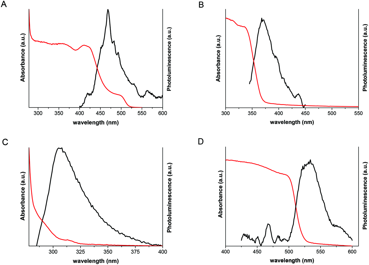 | ||
| Fig. 6 Emission and absorbance spectra of the lead halides. (A), PbI2-P3m1; (B), PbBr2; (C), PbCl2; (D), PbI2-Pm1. | ||
The possible reason for the existence of such structure in PbI2 nanosheets may be the fast formation mechanism which leads to 20 nm thick nanosheets, presumably accompanied with planar defect formation and vacancy agglomeration. With larger reaction periods this complex structure relaxes gradually due to ion migration to lower energy positions in the lattice. These gradual changes can be observed both by XRD and PL/UV-Vis spectroscopy. It is worth noting, that interpolytypic transitions for PbI2 were observed and described by other authors, e.g. Minagawa et al. observed the 4H to 2H transition in PbI2 bulk crystals at room temperature.47 Sengupta with co-authors observed a photodegradation process of PbI2 nanoparticles accompanied by spectral changes in UV-Vis absorption. They assumed the formation of multilayered particles and the existence of energy barriers between the layers.48
PbBr2 nanosheets show one peak for the absorbance at 335 nm and one peak for the PL at 371 nm which corresponds well with the band gap at 3.3 eV (Fig. 6B).49Fig. 6C exhibits the optical results for 2D PbCl2 with the corresponding peaks at 291 nm and 305 nm which also fit well for the band gap at 3.8 eV.50 The structures for PbBr2 and PbCl2 have large thicknesses and as a result of that no confinement can be observed.
4. Conclusion
Until now, it was only possible to synthesize particles of lead iodide with thicknesses of 100 nm and larger. Here, we demonstrated that it is possible to prepare this material with thicknesses below 100 nm and furthermore to synthesize structures of lead bromide and lead chloride in this range. We also present a chemical mechanism for the formation of PbI2 nanosheets. The two important points are the usage of haloalkanes as source materials for the anions and TOP which increases the reactivity of the synthesis. A fast reaction of the TOP molecules with the haloalkanes leads to the release of anions which can react with the lead oleate complex to form lead halide particles. The shape is formed due to the high amount of oleic acid present in all lead halide syntheses. Insights into structural changes of PbI2 nanosheets during the synthesis are given. We can conclude that the space group change from P3m1 to Pm1 is conditioned by the polytypic transition accompanied with relaxation of the initial defect structure. This influences the spectral properties of synthesized nanosheets and can serve as useful tool for quality control of synthesized 2D materials. The defect and bulk nanosheets can be distinguished by all analytic methods like TEM, XRD, AFM and UV/Vis absorbance and PL spectroscopy as well as DFT simulations. Finally, we extend the 2D family of PbX2 materials presenting the synthesis protocols for PbBr2 and PbCl2 nanosheets with micron-range lateral size. The structures might be interesting for low-cost applications in the field of high-energy detectors or they might serve as base materials for perovskite syntheses.
Conflicts of interest
The authors declare no conflicts of interest.Acknowledgements
The authors thank the German Research Foundation DFG financial support in the frame of the Cluster of Excellence “Center of ultrafast imaging CUI” and for granting the project KL 1453/9-2. The European Research Council is acknowledged for funding an ERC Starting Grant (Project: 2D-SYNETRA (304980), Seventh Framework Program FP7).References
- R. Mas-Balleste, C. Gomez-Navarro, J. Gomez-Herrero and F. Zamora, 2D Materials: To Graphene and Beyond, Nanoscale, 2011, 3, 20–30 RSC.
- C.-Y. Chi, C.-C. Chang, S. Hu, T.-W. Yeh, S. B. Cronin and P. D. Dapkus, Twin-Free GaAs Nanosheets by Selective Area Growth: Implications for Defect-Free Nanostructures, Nano Lett., 2013, 13, 2506–2515 CrossRef CAS PubMed.
- Y. Zhang, M. Shang, Y. Mi, T. Xia, P. Wallenmeyer, J. Murowchick, L. Dong, Q. Zhang and X. Chen, Influence of the Amount of Hydrogen Fluoride on the Formation of (001) Faceted Titanium Dioxide Nanosheets and Their Photocatalytic Hydrogen Generation Performance, ChemPlusChem, 2014, 79, 1159–1166 CrossRef CAS.
- J. Zheng, Y. Cao, J.-R. Fu, C. Chen, C. Cheng, R.-W. Yan, S.-G. Huang and C.-C. Wang, Facile synthesis of magnetic Fe3S4 nanosheets and their application in lithium-ion storage, J. Alloys Compd., 2016, 668, 27–32 CrossRef CAS.
- E. Lhuillier, S. Pedetti, S. Ithurria, B. Nadal, H. Heuclin and B. Dubertret, 2D Colloidal Metal Chalcogenides Semiconductors: Synthesis, Spectroscopy and Applications, Acc. Chem. Res., 2015, 48, 22–30 CrossRef CAS PubMed.
- D. O. Sigle, L. Zhang, S. Ithurria, B. Dubertret and J. J. Baumberg, Ultrathin CdSe in Plasmonic Nanogaps for Enhanced Photocatalytic Water Splitting, J. Phys. Chem. Lett., 2015, 6, 1099–1103 CrossRef CAS PubMed.
- S. Dogan, T. Bielewicz, Y. Cai and C. Klinke, Field–effect transistors made of individual colloidal PbS nanosheets, Appl. Phys. Lett., 2012, 101, 073102 CrossRef.
- Y. T. Lee, W. K. Choi and D. K. Hwang, Chemical free device fabrication of two dimensional van der Waals materials based transistors by using one-off stamping, Appl. Phys. Lett., 2016, 108, 253105 CrossRef.
- P. Agnihotri, P. Dhakras and J. U. Lee, Bipolar Junction Transistors in Two-Dimensional WSe2 with Large Current and Photocurrent Gains, Nano Lett., 2016, 16, 4355–4360 CrossRef CAS PubMed.
- R. Velazquez, A. Aldalbahi, M. Rivera and P. Feng, Fabrications and application of single crystalline GaN for high-performance deep UV photodetectors, AIP Adv., 2016, 6, 085117 CrossRef.
- S. Oh, J. Kim, F. Ren, S. J. Pearton and J. Kim, Quasi-two-dimensional β-Gallium Oxide Solar-blind Photodetectors with Ultrahigh Responsivity, J. Mater. Chem., 2016, 10, 1039 Search PubMed.
- S. Dogan, T. Bielewicz, V. Lebedeva and C. Klinke, Photovoltaic effect in individual asymmetrically contacted lead sulfide nanosheets, Nanoscale, 2015, 7, 4875 RSC.
- T. Bielewicz, S. Dogan and C. Klinke, Tailoring the height of ultrathin PbS nanosheets and their application as field-effect transistors, Small, 2015, 11, 826 CrossRef CAS PubMed.
- S. Vikulov, F. Di Stasio, L. Ceseracciu, P. L. Saldanha, A. Scarpellini, Z. Dang and V. Lesnyak, Fully Solution-Processed Conductive Films Based on Colloidal Copper Selenide Nanosheets for Flexible Electronics, Adv. Funct. Mater., 2016, 26(21), 3670–3677 CrossRef CAS.
- J. N. Coleman, M. Lotya, A. O'Neill, S. D. Bergin, P. J. King, U. Khan, K. Young, A. Gaucher, S. De, R. J. Smith, I. V. Shvets, S. K. Arora, G. Stanton, H.-Y. Kim, K. Lee, G. T. Kim, G. S. Duesberg, T. Hallam, J. J. Boland, J. J. Wang, J. F. Donegan, J. C. Grunlan, G. Moriarty, A. Shmeliov, R. J. Nicholls, J. M. Perkins, E. M. Grieveson, K. Theuwissen, D. W. McComb, P. D. Nellist and V. Nicolosi, Two-Dimensional Nanosheets Produced by Liquid Exfoliation of Layered Materials, Science, 2011, 331, 568–571 CrossRef CAS PubMed.
- R. Ma and T. Sasaki, Nanosheets of Oxides and Hydroxides: Ultimate 2D Charge-Bearing Functional Crystallites, Adv. Mater., 2010, 22, 5082–5104 CrossRef CAS PubMed.
- J.-W. Seo, J.-W. Jun, S.-W. Park, H. Nah, T. Moon, B. Park, J.-G. Kim, Y. J. Kim and J. Cheon, Two-Dimensional Nanosheet Crystals, Angew. Chem., Int. Ed., 2007, 46, 8828–8831 CrossRef CAS PubMed.
- Z. Cui, L. Mi and D. Zeng, Oriented attachment growth of BiOCl nanosheets with exposed facets and photocatalytic activity of the hierarchical nanostructures, J. Alloys Compd., 2013, 549, 70–76 CrossRef CAS.
- M. Safdar, Z. Wang, M. Mirza, F. K. Butt, Y. Wang, L. Sun and J. He, Telluride-based nanorods and nanosheets: synthesis, evolution and properties, J. Mater. Chem. A, 2013, 1, 1427–1432 CAS.
- B. Mukherjee, Y. Cai, H. R. Tan, Y. P. Feng, E. S. Tok and C. H. Sow, NIR Schottky Photodetectors Based on Individual Single-Crystalline GeSe Nanosheet, ACS Appl. Mater. Interfaces, 2013, 5, 9594–9604 CAS.
- J. C. Shaw, H. Zhou, Y. Chen, N. O. Weiss, Y. Liu, Y. Huang and X. Duan, Chemical vapor deposition growth of monolayer MoSe2 nanosheets, Nano Res., 2014, 7, 511 CrossRef CAS.
- K. Xu, Z. Wang, X. Du, M. Safdar, C. Jiang and J. He, Atomic-layer triangular WSe2 sheets: synthesis and layer-dependent photoluminescence property, Nanotechnology, 2013, 24, 465705 CrossRef PubMed.
- M. D. Khan, J. Akhtar, M. A. Malik, M. Akhtarac and N. Revaprasadu, Phase-pure fabrication and shape evolution studies of SnS nanosheets, New J. Chem., 2015, 39, 9569–9574 RSC.
- S. Lee, D. T. Lee, J.-H. Ko, W.-J. Kim, J. Joo, S. Jeong, J. A. McGuire, Y.-H. Kim and D. C. Lee, Slow colloidal growth of PbSe nanocrystals for facile morphology and size control, RSC Adv., 2014, 4, 9842–9850 RSC.
- T. Bielewicz, E. Klein and C. Klinke, New ways to synthesize lead sulfide nanosheets-substituted alkanes direct the growth of 2D nanostructures, Nanotechnology, 2016, 27, 355602 CrossRef PubMed.
- A. Nag, M. V. Kovalenko, J.-S. Lee, W. Liu, B. Spokoyny and D. V. Talapin, Metal-free Inorganic Ligands for Colloidal Nanocrystals: S2−, HS−, Se2−,HSe−, Te2−, HTe−, TeS32−, OH−, NH2− as Surface Ligands, J. Am. Chem. Soc., 2011, 133, 10612–10620 CrossRef CAS PubMed.
- F. Hussain, C. Ritchie, R. W. Gable, B. Moubaraki, K. S. Murray and C. Boskovic, Tungstoarsenate(III) polyoxoanions as inorganic ligands for polynuclear copper complexes, Polyhedron, 2009, 28, 2070–2074 CrossRef CAS.
- D. I. Garcia-Gutierrez, L. M. De Leon-Covian, D. F. Garcia-Gutierrez, M. Trevino-Gonzalez, M. A. Garza-Navarro and S. Sepulveda-Guzman, On the role of Pb0 atoms on the nucleation and growth of PbSe and PbTe nanoparticles, J. Nanopart. Res., 2013, 15, 1620 CrossRef.
- M. Chen, Y.-G. Feng, X. Wang, T.-C. Li, J.-Y. Zhang and D.-J. Qian, Silver Nanoparticles Capped by Oleylamine: Formation, Growth, and Self-Organization, Langmuir, 2007, 23, 5296–5304 CrossRef CAS PubMed.
- B. H. Juarez, The Role of Halogens in the Synthesis of Semiconductor Nanocrystals, Z. Phys. Chem., 2014, 229, 119–137 Search PubMed.
- A. Ferreira da Silva, N. Veissid, C. Y. An, I. Pepe, N. Barros de Oliveira and A. V. Batista da Silva, Optical determination of the direct bandgap energy of lead iodide crystals, Appl. Phys. Lett., 1996, 69, 1930–1932 CrossRef CAS.
- Y.-C. Chang and R. B. James, Phonon dispersion and polar-optical scattering in 2H PbI2, Phys. Rev. B: Condens. Matter Mater. Phys., 1997, 55, 8219 CrossRef CAS.
- M. Y. Khilji, W. F. Sherman and G. R. Wilkinson, Raman Study of Three Polytypes of PbI2, J. Raman Spectrosc., 1982, 13, 127 CrossRef CAS.
- R. S. Mitchell, Structural polytypism of lead iodide and its relationship to screw dislocations, Z. Kristallogr.-Cryst. Mater., 1959, 111.1–6, 372–384 CrossRef.
- L. Protesescu, S. Yakunin, M. I. Bodnarchuk, F. Krieg, R. Caputo, C. H. Hendon, R. X. Yang, A. Walsh and M. V. Kovalenko, Nanocrystals of Cesium Lead Halide Perovskites (CsPbX3, X=Cl, Br, and I): Novel Optoelectronic Materials Showing Bright Emission with Wide Color Gamut, Nano Lett., 2015, 15, 3692–3696 CrossRef CAS PubMed.
- J. S. Steckel, B. K. H. Yen, D. C. Oertel and M. G. Bawendi, On the Mechanism of Lead Chalcogenide Nanocrystal Formation, J. Am. Chem. Soc., 2006, 128, 13032–13033 CrossRef CAS PubMed.
- J. Joo, J. M. Pietryga, J. A. McGuire, S.-H. Jeon, D. J. Williams, H.-L. Wang and V. I. Klimov, A Reduction Pathway in the Synthesis of PbSe Nanocrystal Quantum Dots, J. Am. Chem. Soc., 2009, 131, 10620–10628 CrossRef CAS PubMed.
- C. M. Evans, M. E. Evans and T. D. Krauss, Mysteries of TOPSe Revealed: Insights into Quantum Dot Nucleation, J. Am. Chem. Soc., 2010, 132, 10973–10975 CrossRef CAS PubMed.
- P. Scherrer, Nachr. Ges. Wiss. Goettingen, Math.-Phys. Kl., 1918, 2, 98 Search PubMed.
- V. K. Agrawal, G. K. Chadha and G. C. Trigunayat, Crystal structures of three polytypes of lead iodide: Correlation between phenomena of arcing and polytypism, Acta Crystallogr., Sect. A: Found. Crystallogr., 1970, 26.1, 140–144 CrossRef.
- P. C. Jain and G. C. Trigunayat, On Centrosymmetric Space Groups in Close-Packed MX2-Type Structures, J. Catal., 2017, 346, 10–20 CrossRef.
- M. A. Shah and M. A. Wahab, Growth rate and symmetry of polytypes in MX2-compounds, J. Mater. Sci. Lett., 2000, 19, 1813–1816 CrossRef CAS.
- C. Schliehe, B. H. Juarez, M. Pelletier, S. Janderz, D. Greshnykh, M. Nagel, A. Meyer, S. Föerster, A. Kornowski, C. Klinke and H. Weller, Ultrathin PbS Sheets by Two-Dimensional Oriented Attachment, Science, 2010, 329, 550–553 CrossRef CAS PubMed.
- G. K. Kasi, N. R. Dollahon and T. S. Ahmadi, Fabrication and characterization of solid PbI2 nanocrystals, J. Phys. D: Appl. Phys., 2007, 40, 1778–1783 CrossRef CAS.
- T. S. Moss, The interpretation of the properties of indium antimonide, Proc. Phys. Soc., London, Sect. B, 1954, 67, 775–782 CrossRef.
- E. Burstein, Anomalous optical absorption limit in InSb, Phys. Rev., 1954, 93, 632–633 CrossRef CAS.
- T. Minagawa, Common polytypes of PbI2 at low and high temperatures and the 2H-12R transformation, Acta Crystallogr., Sect. A: Found. Crystallogr., 1975, 31(6), 823–824 CrossRef.
- A. Sengupta, K. C. Mandal and J. Z. Zhang, Ultrafast electronic relaxation dynamics in layered iodide semiconductors: a comparative study of colloidal BiI3 and PbI2 Nanoparticles, J. Phys. Chem. B, 2000, 104(40), 9396–9403 CrossRef CAS.
- M. J. Weber, Handbook of Optical Materials, J. Phys. D: Appl. Phys., 2003, 40, 87 Search PubMed.
- M. Iwanaga, T. Hayashi, M. Shirai and K. Tanaka, Self-trapped states and related luminescence in PbCl2 crystals, Phys. Rev. B: Condens. Matter, 2002, 66, 064304 CrossRef.
Footnote |
| † Electronic supplementary information (ESI) available. See DOI: 10.1039/c7nr09564c |
| This journal is © The Royal Society of Chemistry 2018 |