
 Open Access Article
 This Open Access Article is licensed under a
 Creative Commons Attribution 3.0 Unported Licence
Tunable laser interference lithography preparation of plasmonic nanoparticle arrays tailored for SERS†
Nestor
Gisbert Quilis
a,
Médéric
Lequeux
 bc,
Priyamvada
Venugopalan
a,
Imran
Khan
ad,
Wolfgang
Knoll
a,
Souhir
Boujday
c,
Marc
Lamy de la Chapelle
be and
Jakub
Dostalek
*a
bc,
Priyamvada
Venugopalan
a,
Imran
Khan
ad,
Wolfgang
Knoll
a,
Souhir
Boujday
c,
Marc
Lamy de la Chapelle
be and
Jakub
Dostalek
*a
aBiosensor Technologies, AIT-Austrian Institute of Technology GmbH, Konrad-Lorenz-Strasse 24, 3430 Tulln, Austria. E-mail: Jakub.dostalek@ait.ac.at
bUniversité Paris 13, Sorbonne Paris Cité, Laboratoire CSPBAT, CNRS, UMR 7244, 74 rue Marcel Cachin, 93017 Bobigny, France
cSorbonne Université, CNRS, UMR 7197, Laboratoire de Réactivité de Surface, LRS, F75252 Paris, France
dAIT-Austrian Institute of Technology, Center for Energy, Photovoltaic Systems, Giefinggasse 2, A-1210 Vienna, Austria
eInstitut des Molécules et Matériaux du Mans (IMMM - UMR CNRS 6283), Avenue Olivier Messiaen, 72085 Le Mans cedex 9, France
First published on 23rd May 2018
Abstract
The facile preparation of arrays of plasmonic nanoparticles over a square centimeter surface area is reported. The developed method relies on tailored laser interference lithography (LIL) that is combined with dry etching and it offers means for the rapid fabrication of periodic arrays of metallic nanostructures with well controlled morphology. Adjusting the parameters of the LIL process allows for the preparation of arrays of nanoparticles with a diameter below hundred nanometers independently of their lattice spacing. Gold nanoparticle arrays were precisely engineered to support localized surface plasmon resonance (LSPR) with different damping at desired wavelengths in the visible and near infrared part of the spectrum. The applicability of these substrates for surface enhanced Raman scattering is demonstrated where cost-effective, uniform and reproducible substrates are of paramount importance. The role of deviations in the spectral position and the width of the LSPR band affected by slight variations of plasmonic nanostructures is discussed.
Introduction
Metallic nanostructures exhibiting localized surface plasmon resonance (LSPR) are attracting increasing attention in numerous fields that can benefit from their extraordinary optical properties. These particularly include research in nanophotonics1,2 and their applications for light management in thin film devices,3,4 amplified optical spectroscopy, and analytical technologies.5,6 These nanostructures possess the capability to couple light energy to localized surface plasmons (LSPs), which originate from collective oscillations of electron density and associated electromagnetic field. The excitation of these modes leads to enhanced absorption, scattering and sub-wavelength confinement of light energy at narrow spectral windows. These phenomena are accompanied by strongly increased electromagnetic field intensity, which is attractive for amplifying weak spectroscopic signals such as Raman scattering, fluorescence, and infrared absorption spectroscopy. Enhancement factors up to several orders of magnitudes were reported to open the door for the ultrasensitive detection of chemical and biological species.7,8In the past decades, nanotechnology research took advantage of rapidly advancing fabrication methods with gradually improved precision and control in the preparation of nanostructured materials. Electron beam lithography and focused ion beam milling9–11 positioned themselves as irreplaceable tools in the nanophotonics research domain and are routinely used for the fabrication of plasmonic nanostructures with tailored morphology. However, these techniques do not allow fully harnessing the potential of such materials in practical applications. The reasons are that they are not suitable for scaled up production due to their limited throughput, costly instrumentation and are capable of patterning only small areas. In order to overcome these drawbacks, other methods for nanoscale patterning that are simpler and cost-effective have been pursued. These include nanoimprint lithography, which offers the means for repeated replicating of nanoscale features by using a working stamp casted from a pre-fabricated master.12–14 Other techniques were developed based on the self-assembly of building blocks forming nanoscale periodic features that can be employed as a lithographic mask.15–17 This approach was utilized in nanosphere lithography or block copolymer lithography for large area structuring; however, it lacks long range order and suffers from edge defects and lower homogeneity.18 Chemically synthesized metallic nanoparticles can be assembled into tailored plasmonic nanostructures by using atomic force microscopy19 or, for instance, end-to-end coupling of metallic nanorods was reported for the preparation of dimers with the use of selective local modification of end tips.20 Interestingly, chemically synthesized gold nanoparticles were infiltrated into a three-dimensional network of polymer fibers to increase their surface density compared to two-dimensional architectures and to take advantage of their hydrophobic properties.21 In addition, natural materials carrying hierarchical micro-nano-structures (e.g. rose petal, taro leaf and lotus leaf) were coated with metal and demonstrated to serve as low-cost SERS-active substrates with superhydrophobic properties enabling efficient enrichment of chemical and biological species to specific areas probed with intense electromagnetic field intensity.22,23
Laser interference lithography (LIL) represents an alternative method that is suitable for the preparation of periodic nanoscale features with controlled size and shape.24–26 LIL techniques offer the advantage of mass production-compatible preparation27,28 and represent an attractive means for (arguably) the simple and fast patterning of large areas of up to hundreds of square centimeters. LIL utilizes the recording of an interference field pattern into a photosensitive resist material29,30 and in combination with lift-off or ion etching steps, it can be used for the preparation of arrays of metallic nanoparticles. For the lift-off approach, metallic nanoparticles are made by depositing a metal inside cavities formed in a photosensitive resist, which is subsequently removed by a solvent.31 In this variant of the LIL approach, the size of metallic nanoparticles is controlled by the cavity diameter that is typically proportional to the period length.32–34 The employment of a sacrificial layer is frequently required in order to facilitate the lift-off as it is often limited by the steepness of the cavity sidewalls.35,36 The ion etching modality employs a nano-patterned resist that serves as a mask on the top of a metallic layer. This mask is transferred to the metal by a dry etching step, which attacks areas that are not protected by the resist material.37–40 In both approaches, the tuning of LSPR on prepared arrays of metallic nanoparticles has been mainly achieved by changing the angle θ between the interfering beams upon the recording of the mask. Then both the period and diameter of metallic nanoparticles are varied and thus not all geometrical combinations are accessible. In addition, lift off-based LIL implementations are typically not suitable for the preparation of features with size below hundred nanometers unless very small periods of the arrays are prepared or complex systems such as extreme ultraviolet LIL with a beam emitted from a synchrotron are employed.41,42
Plasmonic nanostructures need to be carefully engineered to couple light at specific wavelength bands42,43 for specific applications. This requires highly tunable nanofabrication methods as plasmonic properties of arrays of metallic nanoparticles strongly depend on multiple parameters including particle size, shape, and inter-particle distance.43,44 This paper reports on the LIL implementation that enables the highly versatile preparation of arrays of cylindrical metallic nanoparticles with independent control of their diameter and period. In addition, diameters below hundred nanometers can be achieved. The importance of such versatility is illustrated in an experiment where gold nanoparticle arrays that are resonant in the red and infrared part of the spectrum are tailored to serve as SERS substrates.
Results and discussion
Preparation of gold nanoparticle arrays over a large area
The LIL set-up employed in the reported experiments utilized a Lloyd's mirror configuration that is depicted in Fig. 1(a). The period of rectangular arrays of metallic nanoparticles Λ was controlled by the angle of two collimated interfering beams θ hitting a photoresist layer. In order to prepare 2D arrays of metallic nanoparticles, the exposure was performed twice with the substrate rotated by 90° along the axis perpendicular to its surface. The period Λ decreases when increasing the angle θ according to the formula Λ = λ/2 sin(θ), where λ = 325 nm is the wavelength of herein used coherent interfering beams. It is worth noting that the structured illuminated area depends on the length of the mirror LM and in the reported setup it was about 2 cm. (Alternatively, another LIL configuration where the beam is split into two equal parts that are recombined over the resist surface can be used. Such a set-up allows for recording over a larger area but the configuration is more sensitive to fluctuations and more complex to align.26) The two exposures of interfering collimated beams form the pattern that is simulated in Fig. 1(b). For the used positive photoresist, the area exposed to high recording light intensity can be etched upon the subsequent development step. By controlling the development time tdev, the photoresist layer can be fully removed from the exposed area to yield a mask in the form of periodic arrays of resist features. Optimized dose and dilution of the developer enable fine control over the process to create a homogeneous mask with arrays of cylindrically shaped photoresist objects. Afterwards, directional ion milling with argon ions is utilized in order to transfer these features to the gold layer that was deposited underneath the photoresist film. The regions that are not protected by the photoresist are etched away forming gold nanoparticles. The remaining photoresist on top of the gold nanoparticles is then removed with a gentle oxygen plasma treatment of the surface, resulting in regular gold nanoparticle arrays covering macroscopic areas. The fabrication process is briefly illustrated in Fig. 1c and an example of the prepared glass substrate with arrays of metallic nanoparticles is shown in Fig. 1d. An atomic force microscopy study (included in the ESI†) confirms that the oxygen plasma reduces the height of nanostructures by about 20 nm because of the removal of the residual photoresist mask. The height of metallic nanoparticles is 55–60 nm, which is slightly above the thickness of the deposited Au film due to the effect of weak etching into the glass substrate.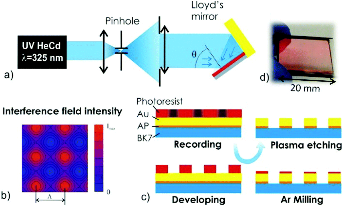 | ||
| Fig. 1 (a) Schematic of the Lloyd's mirror interferometer setup used for the LIL-based recording. (b) Simulations of the field intensity profile recorded for the photoresist. (c) Development of the photoresist and dry etching of Au NP arrays on a substrate with a thin adhesion promoter (AP). (d) Example of prepared gold nanoparticle arrays on a BK7 glass substrate with the size of 20 × 20 mm2. | ||
Tunability of the localized surface plasmon resonance
Gold nanoparticle arrays with a period between Λ = 260 nm and 560 nm were prepared by varying the interference angle θ in the LIL recording step. In order to tune the diameter of nanoparticles D, the exposure dose was kept constant at 6.75 mJ cm−2 and the development time tdev was varied. As illustrated in Fig. 2a, arrays of holes are prepared in the gold film for the short development time tdev = 95 s. On increasing the development time to tdev = 110 s, arrays of rectangular-shaped, not connected nanoparticles are observed in Fig. 2b. Further prolonging the development time from tdev = 165 to 220 s yields arrays of cylindrical gold nanoparticles with diameters decreasing from D = 185 to 85 nm, see Fig. 2c–e. The resonant coupling to LSPs supported by prepared gold nanoparticle arrays is manifested as a narrow dip in the transmission spectrum as shown in Fig. 2(f). The wavelength at which the minimum of the dip occurs (λLSPR) shifts towards the near infrared (NIR) part of the spectrum when increasing the diameter D. For example, LSPR can be tuned in the spectral window λLSPR = 700–900 nm by changing the diameter from D = 85 to 350 nm for the showed period of Λ = 460 nm. | ||
| Fig. 2 SEM images of metallic arrays with nanoscale features for varied development time tdev and fixed period of Λ = 460 nm. (a) Nanohole arrays for tdev = 95 s; (b) diamond-shaped nanoparticle arrays for tdev = 110 s, and arrays of cylindrical nanoparticles for (c) tdev = 165 s, D = 185 nm; (d) tdev = 195 s, D = 115 nm; (e) tdev = 220 s, D = 85 nm. (f) Transmission spectra measured for indicated gold disk diameters D and period Λ = 460 nm by collimated beam illuminating area of about 0.5 mm2. | ||
In general, the LSPR wavelength λLSPR on gold nanoparticle arrays is a function of both period Λ and diameter D. Its shift towards longer wavelengths by increasing the diameter D is more pronounced for longer periods Λ. This can be explained by diffraction coupling of LSPs for the interparticle distances that are in the wavelength range of the incident light.45 The possibility of independent control of both period and diameter is demonstrated in Fig. 3. A series of samples with the period varied in the range of Λ = 260–560 nm and diameter D = 70–350 nm were prepared and transmission spectra were recorded. The analysis of these spectra confirms the tuning of the LSPR wavelength λLSPR between 620 and 1050 nm and reveals that identical λLSPR can occur for multiple combinations of Λ and D.
 | ||
| Fig. 3 Measured dependence of the resonant wavelength λLSPR on the diameter D and period between Λ of gold nanoparticle arrays in contact with air. | ||
Homogeneity of the prepared nanoparticle arrays
In order to characterize the spatial homogeneity of plasmonic properties of prepared nanostructures, we performed a mapping of the spectral position and width of LSPR bands on two substrates carrying gold nanoparticle arrays with Λ = 400 nm and D = 215 nm (S1) and Λ = 500 nm and D = 165 nm (S2). Fig. 4 shows an example of the LSPR transmission spectra acquired from a series of spots on the substrate S1 and from such a type of spectra, variations in the resonant wavelength λLSPR and the width of the full width in the half minimum ΔλFWHM were determined. | ||
| Fig. 4 Comparison of LSPR spectra measured on substrate S1 after functionalization with 4-mercaptobenzoic acid on (a) a series of spots with a large 1 mm diameter arranged over 1 × 1 cm with collimated beam and (b) with focused beam diameter 3 μm scanned over 200 × 200 μm. The dashed line in (b) shows the transmission spectrum measured with a large diameter beam on the same sample for comparison. | ||
Firstly, let us discuss the measurements performed by using a collimated beam that exhibits a diameter of about 1 mm and which was scanned over arrays of spots arranged on an area of 1 × 1 cm2. The determined mean LSPR wavelength λLSPR and the width ΔλFWHM are summarized in Table 1 for both substrates S1 and S2. The mean value and standard deviation of these parameters yield λLSPR = 782 ± 4 nm and ΔλFWHM = 221 ± 15 nm for substrate S1. On the second substrate S2 with a longer period, an almost identical spectral position of λLSPR = 782 ± 5 nm and narrower resonance ΔλFWHM = 106 ± 2 nm were observed (see the ESI†).
| Substrate | λ LSPR [nm] | ΔλFWHM [nm] | I(ΔλR1) [counts] | I(ΔλR2) [counts] |
|---|---|---|---|---|
| S1, Λ = 400 nm, D = 215 ± 6 nm | 770 ± 13 (782 ± 4) | 172 ± 12 (221 ± 15) | 254 ± 52 | 248 ± 73 |
| S2, Λ = 500 nm, D = 165 ± 8 nm | 787 ± 7 (782 ± 5) | 122 ± 14 (106 ± 2) | 66 ± 15 | 68 ± 18 |
Afterwards, the transmission spectra were measured using a confocal microscope at a series of spots with a smaller diameter of about 3 μm. Interestingly, for substrate S1 the spectral width of such LSPR spectra ΔλFWHM was significantly lower and the variations in the spectral position λLSPR were more pronounced than for the data measured with a large diameter beam (compare examples presented in Fig. 4b and a). When probing this smaller area, the spectral position of λLSPR = 770 ± 13 nm and the resonance width of λFWHM = 172 ± 12 nm were determined. For substrate S2, similar variations in the spectral position of λLSPR = 787 ± 7 nm were measured; however, wider resonances λFWHM = 122 ± 14 were observed with a focused beam compared to a large diameter beam. This effect can be ascribed to the proximity of the diffraction edge, which is visible in the transmission spectra measured by a collimated large diameter beam and which becomes smeared by the varied angle when performing the measurement with a focused beam (see Fig. S2 in the ESI†).
In general, the variations in the LSPR spectra can be attributed to local deviations in the morphology of gold nanoparticles (particularly diameter D) that are related to imperfections of the LIL fabrication process. The analysis of the AFM data (included in the ESI†) reveals that the diameter D varied with a standard deviation of σ(D) = 6 nm on the S1 substrate and σ(D) = 8 nm for the S2 substrate. From the slope in dependencies D(λLSPR) presented in Fig. 3, it can be obtained that the LSPR wavelength changes with the diameter as ∂λLSPR/∂D = 1 and 1.3 for the prepared gold nanoparticle arrays with period Λ = 400 (S1) and 500 nm (S2), respectively. Therefore, the measured variations in diameter D correspond to standard deviation in the LSPR wavelength of σ(λLSPR) = 6 nm for S1 and σ(λLSPR) = 10 nm for S2. Such values are lower than those experimentally observed when probing an area of about 10 μm2 and this discrepancy can be ascribed to additional effects such as the polycrystalline nature of prepared gold nanoparticles and variations in roughness of the top nanoparticle surface and that of the glass substrate.
Surface enhanced Raman spectroscopy on gold nanoparticle arrays
Arrays of gold nanoparticles can serve as an efficient substrate for the amplification of Raman scattering on a probe molecule when exposed to an intense LSP field. This effect occurs when the resonant wavelength λLSPR is located in the vicinity of the impinging (laser) light λL as well as that of Raman scattered light at specific spectral bands centered at wavelengths λR.46–48 In order to demonstrate the applicability of the used LIL method for SERS, 4-mercaptobenzoic acid (4-MBA) was selected as a probe and the laser wavelength of λL = 785 nm was used (see Fig. 5a). In addition, other molecules including 4-aminothiophenol and 1,2-di(4-pyridyl)ethylene were tested for the SERS measurement as seen in the ESI.† | ||
| Fig. 5 (a) Set of SERS spectra measured at different spots for 4-MBA attached to the S1 substrate (red curve represents the averaged spectrum). (b) LSPR spectra measured on substrates S1 and S2 with a large diameter beam. | ||
It has been previously reported in several studies that the highest SERS enhancement factor on gold nanocylinders occurs with λLSPR located between the λL and (red shifted) Stokes vibrational band of the probe of interest, which has been validated for the visible part of the spectrum.49,50 However, such a rule was found not to be valid for the gold nanoparticles that are resonant in the NIR part of the spectrum. Then the optimum λSPR was observed to be significantly blue shifted with respect to λL.51 This can be partially attributed to the blue-shift of the maximum extinction (measured in far field) compared to the wavelength where the strongest enhancement in the near field occurs.52–54 Another important factor is a decrease of the near field intensity for nanoparticles with a larger diameter, supporting resonance in the NIR part of the spectrum compared to that for resonances in the visible,47 and related more complex spectral dependence of the near field enhancement.55
Finite difference time domain (FDTD) simulations were carried out in order to elucidate the spectral dependence of Raman scattering efficiency on the prepared arrays of gold cylindrical nanoparticles. The plasmonically enhanced field intensity strength at laser wavelength λL and Raman band wavelengths λR were simulated in order to evaluate changes in the Raman scattering efficiency that is proportional to the term ∼|E(λL)|2|E(λR)|2. As illustrated by the experimental data in Fig. 3, various combinations of period Λ and diameter D can be chosen to tune λLSPR on arrays of gold cylindrical nanoparticles close to the wavelength λL. Furthermore, a set of four pairs of period Λ and nanoparticle diameter D that define a geometry exhibiting λLSPR close to wavelength λL = 785 nm were selected. The determined geometrical parameters that are specified in the inset of Fig. 6a agree well with those determined experimentally (see Fig. 3). The simulated transmission spectra presented in Fig. 6a show that when increasing the period Λ and decreasing the diameter D, the spectral width of the LSPR band decreases as the experimental data revealed. The spectral width of the resonant feature is a signature of LSP damping that directly affects the electromagnetic field enhancement. For the simulated geometries, the enhancement of electric field amplitude |E|/|E0| was obtained from near-field plots (see an example in the inset of Fig. 6b) and it was averaged over the surface of a nanoparticle at 2 nm distance from its walls. At the wavelength λL = 785 nm, the averaged electric field amplitude enhancement |E|/|E0| rapidly increases with the period Λ while for the longer wavelengths λR = 850 and 900 nm, the increase of |E|/|E0| is slower, see Fig. 6. These simulations predict that the Raman scattering efficiency at these wavelengths λR (proportional to |E(λL)|2|E(λR)|2) is about 9 times higher for the period Λ = 500 nm than for Λ = 400 nm.
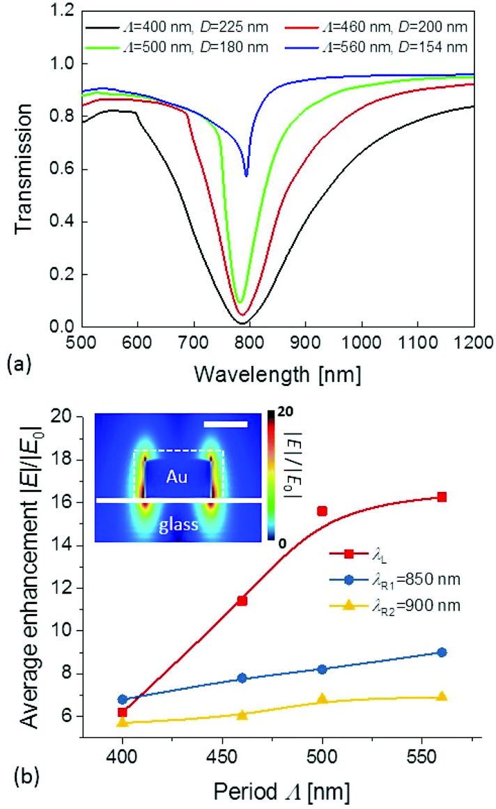 | ||
| Fig. 6 (a) Simulated LSPR transmission spectra for combinations of Λ and D ensuring λLSPR ∼ 800 nm. (b) Dependence of the average electric field amplitude enhancement |E|/|E0| on the nanostructure period Λ for wavelength λL, and λR = 850 and 900 nm. The inset shows an example of simulated near field intensity for Λ = 560 nm with a dashed line representing the surface over which the field amplitude was averaged. All data were obtained for normally incident waves. | ||
In following experiments, two substrates with the period Λ = 400 nm (S1) and 500 nm (S2) were used for SERS measurements of 4-MBA. On these substrates, the diameter of the nanoparticle arrays was adjusted to D = 215 nm and 165 nm, respectively, in order to set LSPR to the desired spectral region close to 785 nm. As can be seen in Fig. 5b and summarized in Table 1, the mean LSPR wavelength on both substrates is almost identical (λLSPR ∼ 782 nm as determined by transmission measurements with a collimated beam) but their resonance width substantially differs. The denser nanoparticle arrays with D = 215 nm show a wider resonance with ΔλFWHM = 172 nm, while the sparser arrays support narrower LSPR with ΔλFWHM = 122 nm. In order to evaluate the strength and homogeneity of the SERS signal on the prepared LIL substrates, the focused laser beam at λL was scanned over their surface after 4-MBA was attached. A series of spots on a grid with 50 μm spacing were evaluated on substrates S1 and S2. On every spot, the Raman spectrum was acquired when irradiating an area with a diameter of about 1 μm (to which the beam at λL was focused) followed by the recording of the LSPR transmission spectrum at the same location (with a diameter of 3 μm defined by the hole in the used confocal microscope). As can be seen in an example presented in Fig. 5a, the measured Stokes vibrational Raman spectra exhibit two strong bands attributed to the probe 4-MBA molecule located at wavelengths shifted by ΔλR1 = 1077 cm−1 (corresponding to λR1 = 857 nm) and by ΔλR2 = 1588 cm−1 (corresponding to λR2 = 896 nm).
The obtained SERS intensities are summarized in Table 1 and firstly, one can see that the average SERS peak intensity on S1 is about 3.7 fold higher than that on the S2 substrate. This observation is in stark contrast to performed FDTD simulations that predict that the longer period substrate S2 enhances the Raman scattering efficiency 9-times stronger than the S1 substrate. This discrepancy can be only partially explained by about a two-fold larger area of the cylindrical nanoparticles (normalized by the unit cell area) on the S1 substrate, which can thus accommodate more target analytes. In addition, weaker coupling strength and wider LSP resonance (see Fig. 5b) were experimentally observed on S2 (see Fig. 5b) compared to the simulations (see Fig. 6a), which also decrease the SERS signal on this substrate. However, very probably also other parameters such as roughness, which was not taken into account in the model, play an important role.
Secondly, there can be seen that when scanning the laser beam over the surface of S1 and S2 substrates, a standard deviation of SERS peak intensity of 20–30% of the mean value occurs. These variations in SERS peak intensity can be mainly attributed to local changes in the LSPR wavelength λLSPR. It is worth noting that probing the area with a diameter of 1 μm corresponds to the excitation of LSPs on ∼3 nanoparticles, which approaches the situation when individual nanoparticles are monitored.56 Thus, even stronger variations in LSPR can be expected than those observed in transmission measurements on ensembles of about 106 nanoparticles carried on an area of 1 mm2 and of 30 nanoparticles carried on 10 μm2 area (see Fig. 4 and Table 1).
Experimental
Materials
A S1805 G2 positive photoresist and AZ 303 developer were purchased from Micro Resist Technology (Germany). Propylene glycol monomethyl ether acetate was obtained from Sigma-Aldrich (Germany). Mercaptobenzoic acid, 4-aminothiophenol and 1,2-di(4-pyridyl)ethylene were acquired from Sigma Aldrich (France).Preparation of gold nanoparticle arrays
A 2 nm thick chromium layer (adhesion layer) and a 50 nm thick gold layer were sequentially prepared on clean glass microscope slides (20 × 20 mm2). Both metals were deposited by thermal evaporation (HHV AUTO 306 from HHV Ltd) under a pressure better than 2 × 10⁻⁶ mbar. Glass substrates were spin-coated at 4500 rpm for 45 s using a Microposit S1805 G2 positive photoresist diluted (1![[thin space (1/6-em)]](https://www.rsc.org/images/entities/char_2009.gif) :2) with propylene glycol monomethyl ether acetate, originating a 100 nm thick film. Afterwards, substrates were soft baked at 100 °C on a hot plate for 120 s. Prior to the exposure, a black tape was attached on the back side of the glass substrates in order to avoid back reflection of the recorded beam. Then, substrates were mounted to the Lloyd's mirror interferometer. Exposure was carried out utilizing a 4 mW HeCd laser (model IK 3031 R-C from Kimmon) at wavelength λ = 325 nm. A spatial filter (×40 microscope lens and pinhole with a diameter of 10 μm) was employed to expand the beam. An additional lens with a focal length of 1 m was used to collimate the beam to the interferometer. The distance between the spatial filter and the sample holder was around 1.8 m. The intensity of the laser beam at the sample holder was found to be 30 μW cm−2. The exposure dose was set to 6.75 mJ cm−2. The periodicity of the particle arrays Λ1 = 260 nm, Λ2 = 300 nm, Λ3 = 400 nm, Λ4 = 460 nm, Λ5 = 500 nm and Λ6 = 560 nm was achieved by adjusting the angle of the interfering beams (θ1 = 38.68, θ2 = 32.80, θ3 = 23.97, θ4 = 20.69, θ5 = 18.97, θ6 = 16.87). After exposure, substrates were immersed in a diluted AZ 303 developer solution with distilled water at a ratio 1:15. Typical developing times were between 90–240 s. Directional dry etching with an argon milling system (Roth & Rau IonSys 500) was carried out to transfer the pattern into the underlying gold layer (etching time 450 seconds, 70 degrees). Finally, the remaining resist was removed using oxygen plasma for 5 minutes, 1 mbar and 40 W.
:2) with propylene glycol monomethyl ether acetate, originating a 100 nm thick film. Afterwards, substrates were soft baked at 100 °C on a hot plate for 120 s. Prior to the exposure, a black tape was attached on the back side of the glass substrates in order to avoid back reflection of the recorded beam. Then, substrates were mounted to the Lloyd's mirror interferometer. Exposure was carried out utilizing a 4 mW HeCd laser (model IK 3031 R-C from Kimmon) at wavelength λ = 325 nm. A spatial filter (×40 microscope lens and pinhole with a diameter of 10 μm) was employed to expand the beam. An additional lens with a focal length of 1 m was used to collimate the beam to the interferometer. The distance between the spatial filter and the sample holder was around 1.8 m. The intensity of the laser beam at the sample holder was found to be 30 μW cm−2. The exposure dose was set to 6.75 mJ cm−2. The periodicity of the particle arrays Λ1 = 260 nm, Λ2 = 300 nm, Λ3 = 400 nm, Λ4 = 460 nm, Λ5 = 500 nm and Λ6 = 560 nm was achieved by adjusting the angle of the interfering beams (θ1 = 38.68, θ2 = 32.80, θ3 = 23.97, θ4 = 20.69, θ5 = 18.97, θ6 = 16.87). After exposure, substrates were immersed in a diluted AZ 303 developer solution with distilled water at a ratio 1:15. Typical developing times were between 90–240 s. Directional dry etching with an argon milling system (Roth & Rau IonSys 500) was carried out to transfer the pattern into the underlying gold layer (etching time 450 seconds, 70 degrees). Finally, the remaining resist was removed using oxygen plasma for 5 minutes, 1 mbar and 40 W.
Morphology measurements
Atomic force microscopy (PicoPlus from Molecular Imaging, Agilent Technologies) was used to investigate the morphology of nanoparticle arrays in the tapping mode. The average diameter was determined by analyzing the grain distribution of nanoparticle arrays using the free Gwyddion software. Additionally, scanning electron microscopy (Zeiss Supra 40 VP SEM) was employed to acquire complementary images.Attachment of SERS-active molecules
LIL-prepared arrays of gold nanoparticles were cleaned with ozone for two hours. Afterwards, the substrate with gold nanoparticles was rinsed with ethanol and immersed in 4-mercaptobenzoic acid, 4-aminothiophenol or 1,2-di(4-pyridyl)ethylene dissolved in ethanol at a concentration of 1 mM for one day in order to form a self-assembled monolayer via reaction by a thiol group or to physisorb on a gold surface. Finally, the substrate was rinsed with ethanol and dried.Optical measurements
Transmission spectra were obtained by using a Bruker Vertex 70 Fourier transform spectrometer (FTIR) with a diameter of the collimated polychromatic beam of 0.5 mm2. In order to perform combined SERS and LSPR experiments with a focused beam, an Xplora Raman microspectrometer (Horiba Scientific, France) with a ×100 objective (numerical aperture of 0.9) was used. On each substrate, several spectra were acquired on a square area of 200 × 200 μm with a distance between neighboring spots of 50 μm. In the case of LSPR measurements, the edge filter was removed and the transmission spectra were measured in the whole spectral range of 400–900 nm. Each spot was illuminated with a white lamp and the recorded spectra were normalized by that acquired on a reference area without the nanostructures. The transmitted light is collected from an area with a diameter of 3 μm defined by the hole of the confocal microscope. The SERS measurements were performed in the backscattering configuration at room temperature with the same lens and a laser beam at λL = 785 nm focused at a spot 1 μm in diameter. The power of the laser beam at the spot was about 100 μW and the Raman spectrum was accumulated by 20 s and artefacts corresponding to cosmic rays were removed. The transmission spectra were analyzed in order to determine the spectral position and the width of the LSPR band.Numerical simulations
In this work, FDTD calculations based on commercial software (FDTD solution, Lumerical Inc., Canada) are employed for simulating the electromagnetic fields around the arrays of gold nanoparticles arranged in a square lattice, taking into account the size of nanoparticles and the spacing between them. A single unit cell of the array, with a uniform mesh size of 2 nm (x, y and z directions), was used to calculate the near field electric intensity and far field transmission spectra. Periodic boundary conditions are applied in the lateral directions while perfectly matched layers are placed above and below the structure in the perpendicular direction to absorb the transmitted and reflected electromagnetic waves. The optical constants of gold are taken from the literature.57 The plane wave source covers a wavelength range of 400 to 950 nm. The structures are studied for the linearly polarized light under the condition of normal incidence.Conclusions
This paper reports on the not yet demonstrated tunability of laser interference lithography for the preparation of gold nanoparticle arrays with precisely controlled geometry enabling tailoring their LSPR characteristics over a broad spectral range. A series of substrates with arrays of cylindrical gold nanoparticles exhibiting an LSPR wavelength in the red and near infrared part of the spectrum were prepared by independently varying the diameter between 70 and 350 nm and period between 260 and 560 nm. Plasmonic substrates with identical LSPR wavelengths tuned to the vicinity of 785 nm and different spectral widths for SERS experiments were prepared. The importance of controlling both the LSPR wavelength and resonance width in order to enhance electromagnetic field intensity at both excitation and Raman scattered wavelength is demonstrated and sources of irregularities that affect the homogeneity of the SERS signal over the substrates are discussed. When probing an area of about millimeter diameter, deviations in the LSPR wavelength and spectral width of about several nanometers were typically observed. Interestingly, when such spectra were measured with a beam focused to a smaller area with a diameter of several microns, these standard deviations substantially increased. Such changes were ascribed to local variations in the morphology of disk-shaped nanoparticles (exhibited standard deviation in diameter of between 3 and 5%), which translate to the SERS signal exhibiting standard deviation between 20 and 30% when scanning over spots with an area of about 1 μm2. The presented methodology provides a tool for the preparation of highly tunable geometries over a large area, opening the door for further development of more complex and efficient plasmonic architectures using the gold nanoparticle arrays as building blocks. In future, this may include engineering of quasi-3D crystals58 where surface plasmons on nanoparticle and nanohole arrays interplay59,60 and support narrow multi-resonant features that potentially overlap with excitation wavelength and Raman scattered wavelength bands.Conflicts of interest
There are no conflicts to declare.Acknowledgements
NGQ acknowledges funding from the European Union's Horizon 2020 research and innovation programme under grant agreement No 642787, Marie Sklodowska-Curie Innovative Training Network BIOGEL, ML and PV from the project jointly funded by Agence Nationale de la Recherche (ANR) and Austrian Science Fund (FWF) under the grant agreements ANR-15-CE29-0026 and I 2647, respectively. IK is grateful for the support from the FWF through the project TRP 304-N20.Notes and references
- M. L. Brongersma, N. J. Halas and P. Nordlander, Nat. Nanotechnol., 2015, 10, 25–34 CrossRef PubMed.
- O. M. Maragò, P. H. Jones, P. G. Gucciardi, G. Volpe and A. C. Ferrari, Nat. Nanotechnol., 2013, 8, 807–819 CrossRef PubMed.
- C. F. Guo, T. Sun, F. Cao, Q. Liu and Z. Ren, Nat. Nanotechnol., 2014, 3, e161 Search PubMed.
- H. A. Atwater and A. Polman, Nat. Mater., 2010, 9, 205–213 CrossRef PubMed.
- C. Valsecchi and A. G. Brolo, Langmuir, 2013, 29, 5638–5649 CrossRef PubMed.
- M. E. Stewart, C. R. Anderton, L. B. Thompson, J. Maria, S. K. Gray, J. A. Rogers and R. G. Nuzzo, Chem. Rev., 2008, 108, 494–521 CrossRef PubMed.
- M. Bauch, K. Toma, M. Toma, Q. Zhang and J. Dostalek, Plasmonics, 2014, 9, 781–799 CrossRef PubMed.
- A. Indrasekara, S. Meyers, S. Shubeita, L. C. Feldman, T. Gustafsson and L. Fabris, Nanoscale, 2014, 6, 8891–8899 RSC.
- K. Ueno and H. Misawa, Phys. Chem. Chem. Phys., 2013, 15, 4093–4099 RSC.
- M. Chirumamilla, A. Gopalakrishnan, A. Toma, R. P. Zaccaria and R. Krahne, Nanotechnology, 2014, 25, 235303 CrossRef PubMed.
- P. Mühlschlegel, H.-J. Eisler, O. Martin, B. Hecht and D. Pohl, Science, 2005, 308, 1607–1609 CrossRef PubMed.
- B. D. Lucas, J. S. Kim, C. Chin and L. J. Guo, Adv. Mater., 2008, 20, 1129–1134 CrossRef.
- L. J. Guo, Adv. Mater., 2007, 19, 495–513 CrossRef.
- S.-W. Lee, K.-S. Lee, J. Ahn, J.-J. Lee, M.-G. Kim and Y.-B. Shin, ACS Nano, 2011, 5, 897–904 CrossRef PubMed.
- D. O. Shin, J.-R. Jeong, T. H. Han, C. M. Koo, H.-J. Park, Y. T. Lim and S. O. Kim, J. Mater. Chem., 2010, 20, 7241–7247 RSC.
- S. Krishnamoorthy, C. Hinderling and H. Heinzelmann, Mater. Today, 2006, 9, 40–47 CrossRef.
- C. Stelling, C. R. Singh, M. Karg, T. A. F. Konig, M. Thelakkat and M. Retsch, Sci. Rep., 2017, 7, 13 CrossRef PubMed.
- C. L. Haynes and R. P. Van Duyne, J. Phys. Chem. B, 2001, 105, 5599–5611 CrossRef.
- P. Moutet, N. M. Sangeetha, L. Ressier, N. Vilar-Vidal, M. Comesana-Hermo, S. Ravaine, R. A. L. Vallee, A. M. Gabudean, S. Astilean and C. Farcau, Nanoscale, 2015, 7, 2009–2022 RSC.
- I. Haidar, G. Levi, L. Mouton, J. Aubard, J. Grand, S. Lau-Truong, D. R. Neuville, N. Felidj and L. Boubekeur-Lecaque, Phys. Chem. Chem. Phys., 2016, 18, 32272–32280 RSC.
- J. D. Shao, L. P. Tong, S. Y. Tang, Z. N. Guo, H. Zhang, P. H. Li, H. Y. Wang, C. Du and X. F. Yu, ACS Appl. Mater. Interfaces, 2015, 7, 5391–5399 Search PubMed.
- S.-Y. Chou, C.-C. Yu, Y.-T. Yen, K.-T. Lin, H.-L. Chen and W.-F. Su, Anal. Chem., 2015, 87, 6017–6024 CrossRef PubMed.
- J.-A. Huang, Y.-L. Zhang, Y. Zhao, X.-L. Zhang, M.-L. Sun and W. Zhang, Nanoscale, 2016, 8, 11487–11493 RSC.
- I. Wathuthanthri, Y. Liu, K. Du, W. Xu and C. H. Choi, Adv. Funct. Mater., 2013, 23, 608–618 CrossRef.
- J.-H. Seo, J. H. Park, S.-I. Kim, B. J. Park, Z. Ma, J. Choi and B.-K. Ju, J. Nanosci. Nanotechnol., 2014, 14, 1521–1532 CrossRef PubMed.
- C. Lu and R. Lipson, Laser Photonics Rev., 2010, 4, 568–580 CrossRef.
- A. Rodriguez, M. Echeverría, M. Ellman, N. Perez, Y. K. Verevkin, C. S. Peng, T. Berthou, Z. Wang, I. Ayerdi, J. Savall and S. M. Olaizola, Microelectron. Eng., 2009, 86, 937–940 CrossRef.
- D. Xia, Z. Ku, S. Lee and S. Brueck, Adv. Mater., 2011, 23, 147–179 CrossRef PubMed.
- A. J. Wolf, H. Hauser, V. Kübler, C. Walk, O. Höhn and B. Bläsi, Microelectron. Eng., 2012, 98, 293–296 CrossRef.
- B. Bläsi, N. Tucher, O. Höhn, V. Kübler, T. Kroyer, C. Wellens and H. Hauser, Proc. SPIE, 2016, 9888, 98880H CrossRef.
- S.-K. Meisenheimer, S. Jüchter, O. Höhn, H. Hauser, C. Wellens, V. Kübler, E. von Hauff and B. Bläsi, Opt. Mater. Express, 2014, 4, 944 CrossRef.
- J.-H. Seo, J. Park, D. Zhao, H. Yang, W. Zhou, B.-K. Ju and Z. Ma, IEEE Photonics J., 2013, 5, 2200106–2200106 CrossRef.
- Y. Oh, J. W. Lim, J. G. Kim, H. Wang, B. H. Kang, Y. W. Park, H. Kim, Y. J. Jang, J. Kim, D. H. Kim and B. K. Ju, ACS Nano, 2016, 10, 10143–10151 CrossRef PubMed.
- M. Schade, B. Fuhrmann, C. Bohley, S. Schlenker, N. Sardana, J. Schilling and H. S. Leipner, J. Appl. Phys., 2014, 115, 084309 CrossRef.
- C. Liu, M. Hong, H. Cheung, F. Zhang, Z. Huang, L. Tan and T. Hor, Opt. Express, 2008, 16, 10701–10709 CrossRef PubMed.
- M. Vala and J. Homola, Opt. Express, 2014, 22, 18778–18789 CrossRef PubMed.
- C. Liu, M. Hong, M. Lum, H. Flotow, F. Ghadessy and J. Zhang, Appl. Phys. A, 2010, 101, 237–241 CrossRef.
- H.-J. Ahn, P. Thiyagarajan, L. Jia, S.-I. Kim, J.-C. Yoon, E. L. Thomas and J.-H. Jang, Nanoscale, 2013, 5, 1836–1842 RSC.
- S. Bagheri, H. Giessen and F. Neubrech, Adv. Opt. Mater., 2014, 2, 1050–1056 CrossRef.
- A. Tsargorodska, O. El Zubir, B. Darroch, M. L. Cartron, T. Basova, C. N. Hunter, A. V. Nabok and G. J. Leggett, ACS Nano, 2014, 8, 7858–7869 CrossRef PubMed.
- W. Karim, S. A. Tschupp, M. Oezaslan, T. J. Schmidt, J. Gobrecht, J. A. van Bokhoven and Y. Ekinci, Nanoscale, 2015, 7, 7386–7393 RSC.
- J. Huang, D. Fan, Y. Ekinci and C. Padeste, Microelectron. Eng., 2015, 141, 32–36 CrossRef.
- C. L. Nehl and J. H. Hafner, J. Mater. Chem., 2008, 18, 2415–2419 RSC.
- E. Petryayeva and U. J. Krull, Anal. Chim. Acta, 2011, 706, 8–24 CrossRef PubMed.
- B. Lamprecht, G. Schider, R. Lechner, H. Ditlbacher, J. Krenn, A. Leitner and F. Aussenegg, Phys. Rev. Lett., 2000, 84, 4721 CrossRef PubMed.
- N. Félidj, J. Aubard, G. Lévi, J. R. Krenn, A. Hohenau, G. Schider, A. Leitner and F. R. Aussenegg, Appl. Phys. Lett., 2003, 82, 3095 CrossRef.
- W. Lee, S. Y. Lee, R. M. Briber and O. Rabin, Adv. Funct. Mater., 2011, 21, 3424–3429 CrossRef.
- N. Guillot and M. L. de la Chapelle, J. Quant. Spectrosc. Radiat. Transfer, 2012, 113, 2321–2333 CrossRef.
- I. Sow, J. Grand, G. Lévi, J. Aubard, N. Félidj, J.-C. Tinguely, A. Hohenau and J. Krenn, J. Phys. Chem. C, 2013, 117, 25650–25658 Search PubMed.
- L. Billot, M. L. de La Chapelle, A.-S. Grimault, A. Vial, D. Barchiesi, J.-L. Bijeon, P.-M. Adam and P. Royer, Chem. Phys. Lett., 2006, 422, 303–307 CrossRef.
- N. Guillot, H. Shen, B. Frémaux, O. Peron, E. Rinnert, T. Toury and M. Lamy de la Chapelle, Appl. Phys. Lett., 2010, 97, 023113 CrossRef.
- B. M. Ross and L. P. Lee, Opt. Lett., 2009, 34, 896–898 CrossRef PubMed.
- P. Alonso-González, P. Albella, F. Neubrech, C. Huck, J. Chen, F. Golmar, F. Casanova, L. Hueso, A. Pucci and J. Aizpurua, Phys. Rev. Lett., 2013, 110, 203902 CrossRef PubMed.
- J. Zuloaga and P. Nordlander, Nano Lett., 2011, 11, 1280–1283 CrossRef PubMed.
- F. J. Colas, M. Cottat, R. Gillibert, N. Guillot, N. Djaker, N. Lidgi-Guigui, T. Toury, D. Barchiesi, A. Toma, E. Di Fabrizio, P. Giuseppe Gucciardi and M. Lamy de la Chapelle, J. Phys. Chem. C, 2016, 120, 13675–13683 Search PubMed.
- M. A. Beuwer, M. W. J. Prins and P. Zijlstra, Nano Lett., 2015, 15, 3507–3511 CrossRef PubMed.
- P. B. Johnson and R. W. Christy, Phys. Rev. Lett. B, 1972, 12, 4370–4379 CrossRef.
- M. E. Stewart, N. H. Mack, V. Malyarchuk, J. Soares, T. W. Lee, S. K. Gray, R. G. Nuzzo and J. A. Rogers, Proc. Natl. Acad. Sci. U. S. A., 2006, 103, 17143–17148 CrossRef PubMed.
- Q. M. Yu, P. Guan, D. Qin, G. Golden and P. M. Wallace, Nano Lett., 2008, 8, 1923–1928 CrossRef PubMed.
- A. Artar, A. A. Yanik and H. Altug, Appl. Phys. Lett., 2009, 95, 051105 CrossRef.
Footnote |
| † Electronic supplementary information (ESI) available. See DOI: 10.1039/c7nr08905h |
| This journal is © The Royal Society of Chemistry 2018 |