
 Open Access Article
 This Open Access Article is licensed under a
 Creative Commons Attribution 3.0 Unported Licence
Patterned tungsten disulfide/graphene heterostructures for efficient multifunctional optoelectronic devices†
A.
Rossi
 ab,
D.
Spirito
c,
F.
Bianco
b,
S.
Forti
a,
F.
Fabbri
a,
H.
Büch
a,
A.
Tredicucci
bd,
R.
Krahne
ce and
C.
Coletti
*ae
ab,
D.
Spirito
c,
F.
Bianco
b,
S.
Forti
a,
F.
Fabbri
a,
H.
Büch
a,
A.
Tredicucci
bd,
R.
Krahne
ce and
C.
Coletti
*ae
aCenter for Nanotechnology Innovation @NEST, Istituto Italiano di Tecnologia, Piazza S. Silvestro 12, 56127 Pisa, Italy. E-mail: camilla.coletti@iit.it
bNEST, Istituto Nanoscienze – CNR and Scuola Normale Superiore, Piazza San Silvestro 12, 56127 Pisa, Italy
cNanochemistry Department, Istituto Italiano di Tecnologia, Via Morego 30, 16163 Genova, Italy
dDipartimento di Fisica “E. Fermi”, Università di Pisa, L.go Pontecorvo 3, 56127 Pisa, Italy
eGraphene Labs, Istituto Italiano di Tecnologia, Via Morego 30, 16163 Genova, Italy
First published on 7th February 2018
Abstract
One of the major issues in graphene-based optoelectronics is to scale-up high-performing devices. In this work, we report an original approach for the fabrication of efficient optoelectronic devices from scalable tungsten disulfide (WS2)/graphene heterostructures. Our approach allows for the patterned growth of WS2 on graphene and facilitates the realization of ohmic contacts. Photodetectors fabricated with WS2 on epitaxial graphene on silicon carbide (SiC) present, when illuminated with red light, a maximum responsivity R ∼220 A W−1, a detectivity D* ∼2.0 × 10⁹ Jones and a −3 dB bandwidth of 250 Hz. The retrieved detectivity is 3 orders of magnitude higher than that obtained with graphene-only devices at the same wavelength. For shorter illumination wavelengths we observe a persistent photocurrent with a nearly complete charge retention, which originates from deep trap levels in the SiC substrate. This work ultimately demonstrates that WS2/graphene optoelectronic devices with promising performances can be obtained in a scalable manner. Furthermore, by combining wavelength-selective memory, enhanced responsivity and fast detection, this system is of interest for the implementation of 2d-based data storage devices.
In the last decade van der Waals (vdW) materials have been in the spotlight of the scientific community, since their two-dimensional (2d) nature allows the direct exploration of electronically confined systems.1 Graphene has been so far the most investigated 2d material and has proven to be a table top choice for fundamental research2 and for applied science.3 However, its lack of bandgap has been a major issue in many applications in electronics and photonics. On the other hand, transition metal dichalcogenides (TMDs) exhibit electronic properties that are complementary to those of graphene, despite sharing the same vdW 2d nature.4,5 The combination in vertical heterostructures of 2d layers has paved the way for a novel device concepts.6 Among TMDs, one of the most interesting is tungsten disulfide (WS2). In its monolayer form, it shows a direct bandgap of 2.1 eV at the two non-equivalent K-points of the Brillouin zone.7 In the vicinity of those points it shows a remarkable splitting of the valence band due to spin–orbit coupling.8,9 Because of symmetry selection rules, spin polarized carriers can be promoted in the conduction band using polarized light.7,10,11 Its optical properties can be used for photodetection to enhance the response of graphene. Indeed, when placed in vertical heterostacks,12 the charge transfer between WS2 and graphene under optical pumping13 was reported to be fast and efficient. Recently, much effort has been devoted to create efficient hybrid TMD/graphene photodetectors.12,14,15 Room temperature photoresponsivities as high as R ∼ 5 × 10⁸ A W−1
![[thin space (1/6-em)]](https://www.rsc.org/images/entities/char_2009.gif) 6 and very fast response times (down to τ = 130 μs)17 have been demonstrated. Yet, one major issue that still has to be efficiently addressed is that of device scalability. Indeed, hybrid photodetectors are generally fabricated using exfoliated TMD/graphene heterostructures. Very recently, photodetectors obtained by combining one layer produced by chemical vapor deposition (CVD) with exfoliated flakes have been reported,17 but although performing well they lack in scalability. Devices fabricated with heterostacks obtained only with CVD grown materials have also been recently proposed.18–20 In De Fazio et al., MoS2 and graphene were separately synthetized via CVD and then transferred on top of each other.20 This approach presents advantages such as the possibility to transfer the heterostack on a selected substrate – either flexible or rigid – and a high photoresponsivity up to hundreds of A W−1.20 However, despite being a large-scale approach, its extension to wafer-scale is complicated by the transfer step.
6 and very fast response times (down to τ = 130 μs)17 have been demonstrated. Yet, one major issue that still has to be efficiently addressed is that of device scalability. Indeed, hybrid photodetectors are generally fabricated using exfoliated TMD/graphene heterostructures. Very recently, photodetectors obtained by combining one layer produced by chemical vapor deposition (CVD) with exfoliated flakes have been reported,17 but although performing well they lack in scalability. Devices fabricated with heterostacks obtained only with CVD grown materials have also been recently proposed.18–20 In De Fazio et al., MoS2 and graphene were separately synthetized via CVD and then transferred on top of each other.20 This approach presents advantages such as the possibility to transfer the heterostack on a selected substrate – either flexible or rigid – and a high photoresponsivity up to hundreds of A W−1.20 However, despite being a large-scale approach, its extension to wafer-scale is complicated by the transfer step.
A possible solution to the abovementioned hurdles has been recently reported in our previous work through the demonstration of the direct scalable synthesis via CVD of continuous mono-bilayer WS2 on epitaxial graphene (EG) on silicon carbide (SiC).11 The WS2 layer synthesized in this way is azimuthally aligned with the underlying EG.9 The precise band alignment and the atomically sharp interfaces of this heterostack are crucial to control the optoelectronic properties of the full structure. In this work, we demonstrate an entirely scalable hybrid WS2/EG photodetector with a maximum photoresponsivity R ∼220 A W−1 under continuous-wave illumination and a −3 dB bandwidth of 250 Hz. The photodetectors also display wavelength-dependent persistent photoconductivity (PPC). The devices were realized with a novel approach for the patterned growth of WS2 on EG, so that WS2 is present only in the active areas for photodetection and the underneath graphene is accessible to metal deposition of ohmic contacts. Indeed, contacting the WS2 directly would generate a Schottky barrier.21 This approach allows minimizing the contact resistance and thus improving the photodetection efficiency.12,15,22
Methods
Synthesis and patterned masking of graphene
EG was grown on nominally on-axis high purity semi-insulating (HPSI) 4H-SiC(0001) substrates (CREE, Inc.) by adapting the approach reported by Emtsev and coworkers23 in an Aixtron HT-BM reaction chamber.24 Before proceeding with WS2 growth, the areas of graphene where contacts shall be subsequently deposited were masked by evaporating 100 nm of gold (Au) (Fig. 1(a)). Au is a highly suitable mask material, because it can sustain high temperatures and it is inert to sulfur (S) atmosphere,25 therefore remaining unaffected during the growth process. The Au mask was obtained using a standard procedure: graphene coating with poly(methyl methacrylate) (PMMA) resist, followed by electron beam lithography (EBL), thermal evaporation of Au and lift-off. It is important to mention that the same results, also in terms of graphene/contacts interface quality, could be achieved using temperature-resistant resist hydrogen silsesquioxane (HSQ) instead of Au mask. This material, once exposed, turns into a film of silicon oxide that can sustain the WS2 growth conditions as well. After the masking phase it can be etched using a 1:5 HF:H2O solution. HSQ offers an alternative to the expensive Au (i.e., for sustaining the high growth temperatures at least 100 nanometers of Au need to be evaporated). The choice of the mask can be dictated by the resistance of the substrate to the mask etchant.
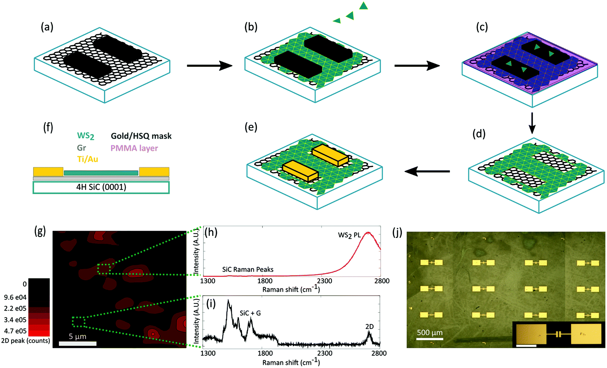 | ||
| Fig. 1 (a) A mask, either Au or HSQ, is deposited on the graphene substrate to prevent the formation of WS2 on selected areas, which allows to (b) obtain full coverage of WS2 outside the mask by the deposition technique described in the text. (c) PMMA is spin coated and patterned to remove the WS2 crystals on top of the mask. (d) The mask is removed either with KI, I2 solution, for Au or HF solution for HSQ. This leaves a pattern behind, on which the contacts can be deposited (e). (f) Legend of the colors used in panels (a)–(e) and side-view of the geometry of the device. (g) Raman/PL map of the active channel with WS2 and graphene and of the contact area with graphene only. The map shows the integrated intensity in the range 2600 cm−1 and 2800 cm−1, in which both the PL of WS2 and graphene 2D peak fall. (h–i) Representative WS2/graphene (h) and graphene only spectra (i). (j) Optical image of a set of devices. The optical contrast observable in the form of “scratches and patches” is due to the backside of the sample, being semi-insulating SiC transparent. Inset showing a zoom-in over device contacts (scale bar 100 μm). | ||
WS2 synthesis
WS2 was synthesized on partially masked graphene (Fig. 1(b)) using a growth process similar to that reported elsewhere.9,11 However, in the present work, the growth recipe was adapted in order to obtain a continuous WS2 monolayer film. Sulfurization of tungsten trioxide (WO3) powder (Sigma Aldrich, 99.995%) was carried out in a horizontal hot-wall furnace (Lenton PTF). The growth temperature within the hot-zone was set to 920 °C and the growth time was 1 h. The EG substrate was placed face-up next to the WO3 powder and within the same crucible. Argon (Ar) was flown during the temperature ramp with a flux of 500 sccm, leading to a pressure of 4.5 mbar, which kept the S solid. After reaching 920 °C, the Ar flux was suddenly reduced to 8 sccm, which reduced the furnace pressure to 0.5 mbar, triggering S evaporation. In order to obtain sudden S evaporation, chalcogen crystals were heated up at 200 °C by wrapping a heating belt around the quartz tube.Device fabrication
After the growth of WS2, some 2d crystals were deposited also on the Au mask (Fig. 1(c)). Removing these crystals before removing the mask is a crucial step to ensure a clean interface with the bare graphene. Therefore, the top surface of the mask was exposed to reactive ion etching with O2 and Ar plasma while protecting the active area by PMMA layer. After a cleaning in acetone, the sample was immersed in a solution of potassium iodide for 3 minutes (H2O:KI:I2 in ratio 40:4:1) in order to remove the Au mask. This allowed for the creation of well-defined channels (Fig. 1(d)) with width of 30 μm and lengths of 2, 5 and 10 μm (device areas 60, 150 and 300 μm2, respectively). If not differently specified, the results reported are relative to devices with shorter channel length, namely 2 μm. Once the WS2/graphene channels were defined, ohmic contacts (source and drain) were fabricated via standard EBL, followed by metal deposition (Ti/Au 10/80 nm) and lift-off (Fig. 1(e)).
Raman and photocurrent measurements
Raman characterization of the synthetized films was carried out with a commercial Renishaw inVia system equipped with a 532 nm green laser. Photocurrent measurements were performed at room temperature in a vacuum probe station from Janis Research (∼2 × 10⁻⁵ mbar). A bias voltage between source and drain contacts was applied up to 2 V. Illumination was provided through an optical window using laser diodes coupled into a fiber and focused on the sample in a spot size of approximately 1 mm, aligned on the devices with micrometer controlled stages. The devices were illuminated with blue (473 nm, 2.62 eV), green (520 nm, 2.38 eV) and red (638 nm, 1.94 eV) lasers. A mechanical shutter was used to block the light passing through the window for dark measurements. Before measuring the photoresponse, current-voltage (IV) characterization in the dark was performed. The photoresponsivity was assessed for photoexcitation intensities ranging from 16 to 680 mW cm−2 both with continuous and temporally modulated light, referred in the following text as DC and AC, respectively. For DC measurements, a Keithley 2600 SMU was used. For AC measurements, the laser light was modulated either by a chopper or by modulating the drive current of the laser diode. The current was measured through a current amplifier, whose output was measured by a lock-in amplifier locked to the modulation signal. Amplification factors, filters and integration times in the amplifiers were tuned according to the frequency and the noise level of the signal. Further photocurrent measurements were also carried out at a wavelength of 532 nm with the Renishaw inVia system used for Raman characterization in order to ensure an illuminating spot size (variable between 1 μm and 15 μm) that is smaller than the device area. A Keithley 2614B SMU was used for current measurements.Results and discussion
The process flow of our fabrication method is depicted in (Fig. 1(a–e)) while the cross section of the measured devices is reported in panel (f). The quality of graphene outside the channels was assessed via Raman spectroscopy prior to contact deposition (Fig. 1(g–i)). Panel (h) and (i) report representative spectra measured inside and outside the channel, respectively. In the channel, the photoluminescence (PL) of WS2 (Fig. 1(h)) is clearly visible and overlapping the Raman signal of graphene (Fig. 1(i)). No appreciable D peak is retrieved and 2D peak position and full width at half maximum (FHWM) are entirely comparable to those of the as-grown material.26 This confirms that the graphene quality is not affected by the processing. Raman and PL spectra of graphene and WS2 as-grown and after processing steps are reported in ESI (Fig. S1†). A Raman map of the main peaks of WS2 – whose position and intensities are indicative of mono-bilayer27,28 thickness – is shown in ESI (Fig. S2†). In Fig. S3,† an AFM image of the patterned area prior to contact deposition is reported, showing a flat graphene surface confining with the WS2/graphene device area. Our fabrication approach allows for the implementation of regular device arrays, as demonstrated in the optical microscope image (Fig. 1(l)). The electrical characterization of the device is reported in Fig. S4† and confirms the ohmic behavior of the graphene-Ti/Au contacts. The effective resistivity, extracted from transfer length measurements (TLM) reported in Fig. S5,† is (1.35 ± 0.08) × 104 Ω μm, which is typical for this kind of samples.29 Both the AFM analysis and the electrical characteristics of the device suggest that our fabrication process results in a clean interface between the graphene and the metal contacts.As the whole patterning and device fabrication processes can also be performed via mask-aligner optical lithography, the reported method can be readily extended to wafer-scale.
Fig. 2(a) reports the device photoresponsivity measured in DC (stars) and AC (diamonds) at 173 Hz for 638 nm illumination at different photoexcitation intensities. The photoresponsivity is calculated using  , where Ipc is the measured photocurrent, Popt is the power incident over the active area. For the AC measurements an additional
  factor is needed to take into account the lock-in amplifier contribution. The photoresponsivity reaches a maximum value of RDC ∼220 A W−1 in DC and RAC ∼36 A W−1 in AC (Fig. 2(a)). The observed difference between AC and DC results can be reasonably attributed to the presence of the EH6/7 trap states within the SiC substrate which, lying at SiC midgap are readily excited with a 638 nm wavelength. Nevertheless, their optical activation occurs on the time scale of tens of seconds and their carrier trap cross section is quite low compared with other SiC trap states.30 This prevents EH6/7 states from affecting AC measurements. For the detectivity, calculated from
  , where A is the active area and Si is the noise spectral density calculated considering thermal noise from dark resistance and shot noise from dark current, we obtain a maximum value (in DC) of D* ∼2.0 × 10⁹ Jones. Such responsivity and detectivity values are promising,15 considering that they are obtained from a vertical heterostack entirely synthetized via CVD. The photoresponse of graphene-only devices is barely detectable at this wavelength (at best RDC ∼0.04 A W−1 (D* ∼5.2 × 10⁵ Jones), see ESI† for measurement details). Hence, the WS2/graphene device manifests an improvement of three orders of magnitude with respect to graphene-only devices. The response time of the devices has been investigated by studying the photoresponsivity signal dependence on the AC frequency, as reported in Fig. 2(b). Despite the non-perfect behavior as RC low-pass filter, the response time of the device can be estimated by using the −3 dB bandwidth figure of merit, i.e. the point at which the signal has dropped to 70% of its initial value.17,31 The obtained value is
  (corresponding to a bandwidth fc = 250 Hz calculated with respect to the maximum value at 20 Hz). To the best of our knowledge, this response time is among the fastest obtained for TMD/graphene devices.15 It is worth of note that a significant signal can be detected also above 10 kHz, where the responsivity is ∼10% of the maximum value. We believe that the clean ohmic contact obtained with our approach is at the basis of the fast response time of our devices. Furthermore the epitaxial relation in our heterostack9 could have a positive impact as well.
 | ||
| Fig. 2 (a) Comparison between photoresponsivity recorded with red light in AC (at 173 Hz) and DC measurements. (b) Normalized photoresponsivity in AC measurement as a function of the frequency, where the light was modulated by a chopper. Measurements where taken at bias voltage of VB = 1.8 V. | ||
In Fig. 3 the wavelength-dependent behavior of the device is reported. Fig. 3(a) shows the WS2/graphene device responsivity in AC at 173 Hz, for three different illumination wavelengths. The responsivities, within the error bars, are generally unaffected by the change in wavelength and, overall, responsivity decreases with increasing light intensity.
 | ||
| Fig. 3 (a) Responsivity vs. power intensity taken at different wavelengths in AC measurements (at 173 Hz). (b) DC measurements of photocurrent at different wavelength as a function of time. PPC progressively disappears with longer wavelength of the excitation light. With each light on/off cycle the light intensity was increased, as indicated by the values above the blue curve. Measurements recorded at a bias voltage VB = 1.8 V. | ||
Fig. 3(b) reports the temporal response of the photocurrent under DC illumination at different wavelengths for on/off cycles with period of 20 s. The three curves collected at different wavelength are offset on the vertical axis for sake of clarity. In this case, the response changes dramatically when we switch from blue (473 nm) to red (638 nm) light. With the excitation at 473 nm once the light is switched off, there is a PPC that remains even on a time scale of hours (see ESI Fig. S6(a)†). The PPC is observed (although to a lesser extent) also for the green illumination, while for excitation with the red laser at 638 nm no PPC is recorded. The incident power dependence has been addressed by increasing the power at each on/off cycle. Although the photocurrent (the number of carriers) increases for all three wavelengths, the dark status is immediately restored for the red one only, even under the highest illumination intensity. This suggests the presence of a slow mechanism that retains the exceeding carriers, which keep accumulating when increasing the power at each cycle. Photocurrent measurements with a smaller illuminating spot (1 μm diameter) on devices with channels of 10 μm width were also carried out and allowed us to exclude the contribution of the contacts to the observed behavior (see ESI, Fig. S7†).
Graphene-only devices displayed the same PPC observed for the WS2/graphene devices (see ESI Fig. S6(b)†). Hence, the observed PPC – differently from what reported in ref. 16 – is not an intrinsic property of the hybrid heterostack. In order to understand the mechanism behind the PPC, the temporal response has been measured when illuminating the WS2/graphene 2 μm device with a spot diameter larger than the channel length, but smaller than the channel width (diameter 15 μm, 532 nm laser). The illumination was switched off only when approaching current saturation. As can be seen in Fig. 4(a), the device shows a slowly decaying “off” current, but after several minutes the dark condition of the device is restored. The observed finite decay is attributed to the smaller illuminated area of the device. Before discussing in detail the measured temporal response of the photocurrent, we analyze the band alignment of our structure, i.e. of the WS2 on epitaxial graphene on 4H-SiC, which we have directly measured via angle-resolved photoemission spectroscopy (ARPES).9 The properties reported in ref. 9 are valid for the case investigated in this work, since the doping level of the epitaxial graphene on hexagonal SiC(0001) is not influenced by the polytype (i.e., 4H or 6H).32 Furthermore, assuming that the HPSI 4H-SiC used as a substrate has the chemical potential at midgap, the total band alignment is the one sketched in Fig. 4(b). The energy band diagram of 4H-SiC is reported on the left, while the graphene cone, schematized in the center, presents the Dirac point 0.4 eV below the Fermi level, a hallmark for EG.33,34 On the right-hand side of panel (b), WS2 bands are reported with the conduction band lying about 260 meV above the Fermi level, as reported for the WS2/EG system.9 HPSI 4H-SiC displays several deep levels (sketched in panel b) with activation energies ranging between 0.7 eV and 0.9 eV below the SiC conduction band,35 which are known to play a fundamental role in the semi insulating behavior of 4H-SiC. These intrinsic deep levels are either acceptor-like levels or negative-U centers generated from C-vacancy complexes (e.g., Z1/2 levels), and act as recombination centers and life-time killers in charge transport experiment.36–38 These defects in the 4H-SiC substrate are responsible for the photogating mechanism in our devices, preventing the decay of the photocurrent. As depicted in Fig. 4(c), if the impinging light has enough energy (i.e. larger than ∼2.2 eV corresponding to a wavelength shorter than 563 nm), it is not only responsible for photocurrent in the WS2/graphene heterostructure, but it also promotes electrons into the aforementioned 4H-SiC deep levels. By acting as recombination centres, such levels capture and neutralize electrons and leave charged holes behind. The accumulated holes generate an electric field that leads to a chemical potential shift in graphene, increasing the number of carriers (Fig. 4(d)). Since the trapping lifetime of these defects is extremely long,39 PPC is observed. Nevertheless, eventually they recombine (Fig. 4(e)), thus the related gate voltage decays and the initial position of the chemical potential is restored. The presence of defect levels with different activation energies is responsible for the distinct behavior observed for blue and green light, e.g. when Z1/2 deep levels are involved, a PPC lasting for several hours is obtained. Red light does not induce any long-lifetime deep level transition,40 and therefore no photogating and no PPC occur. However, the energy of the red light is sufficient to excite the transition from VB to CB in WS2. Subsequently charge transfer from the active layer (WS2) to graphene occurs, injecting carriers in the transport layer (graphene). Hence, the role of WS2 is crucial to enhance the responsivity of the system making the device “active” in the visible range.
 | ||
| Fig. 4 DC photocurrent vs. time using 532 nm excitation wavelength. The curve is taken for two different incident light intensities, at a bias voltage of VB = 1 V. Dimmed-color areas are relative to “light-off” state. (b) Scheme of the band alignment of the system with the relative energies. (c) Scheme of the mechanism involved in the generation of photocurrent and photogating at different wavelengths in the rising part of the signal (red dashed box). (d) Gating effect on graphene from SiC substrate relative to the saturating part of the rising curve (blue dashed box). (e) Recombination in VB occurring with light off in falling curve (gray dashed box). | ||
Conclusion
We reported a novel approach for the implementation of scalable WS2/graphene photoresponsive devices. The use of a mask during the growth is crucial to controllably deposit WS2 just on the optical channel in order to create an effective ohmic contact to the graphene channel. The strength of this approach relies on its flexibility as it can be adopted on different systems, e.g. CVD graphene transferred on SiO2. The presented devices show – when illuminated with red light – a DC responsivity reaching 220 A W−1 and an AC response time of τr ∼0.6 ms. PPC is measured for shorter illumination wavelengths, and a nearly perfect charge retention is observed for blue light. Such PPC originates from deep levels in the SiC substrate. The combination of wavelength-selective memory effect, enhanced responsivity and fast detection is of interest for the fabrication of 2d based optical memories, which might be realized by exploiting a transparent top gate17 to reset the memory state and depopulate the traps.Conflicts of interest
There are no conflicts to declare.Acknowledgements
The authors would like to thank Mirko Rocci from NEST-Scuola Normale Superiore, for fruitful discussion. The research leading to these results has received funding from the European Union's Horizon 2020 research and innovation program under Grant agreement No. 696656 – GrapheneCore1, and under the Marie Skłodowska-Curie Grant Agreement COMPASS No. 691185.References
- A. Kuc, N. Zibouche and T. Heine, Phys. Rev. B: Condens. Matter Mater. Phys., 2011, 83(24), 245213 CrossRef.
- M. I. Katsnelson, K. S. Novoselov and A. K. Geim, Nat. Phys., 2006, 2(9), 620–625 CrossRef CAS.
- K. S. Novoselov, V. I. Fal'ko, L. Colombo, P. R. Gellert, M. G. Schwab and K. Kim, Nature, 2012, 490, 192–200 CrossRef CAS PubMed.
- M. Chhowalla, H. S. Shin, G. Eda, L.-J. Li, K. P. Loh and H. Zhang, Nat. Chem., 2013, 5(4), 263–275 CrossRef PubMed.
- Q. Hua Wang, K. Kalantar-Zadeh, A. Kis, J. N. Coleman and M. S. Strano, Nat. Nanotechnol., 2012, 7, 699–712 CrossRef PubMed.
- A. K. Geim and I. V. Grigorieva, Nature, 2014, 499(7459), 419–425 CrossRef PubMed.
- X. Xu, W. Yao, D. Xiao and T. F. Heinz, Nat. Phys., 2014, 10(5), 343–350 CrossRef CAS.
- M. Dendzik, M. Michiardi, C. Sanders, M. Bianchi, J. A. Miwa, S. S. Grønborg, J. V. Lauritsen, A. Bruix, B. Hammer and P. Hofmann, Phys. Rev. B: Condens. Matter Mater. Phys., 2015, 92(24), 245442 CrossRef.
- S. Forti, A. Rossi, H. Büch, T. Cavallucci, F. Bisio, A. Sala, T. O. Menteş, A. Locatelli, M. Magnozzi, M. Canepa, K. Müller, S. Link, U. Starke, V. Tozzini and C. Coletti, Nanoscale, 2017, 9(42), 16412–16419 RSC.
- P. K. Nayak, F. C. Lin, C. H. Yeh, J. S. Huang and P. W. Chiu, Nanoscale, 2016, 8(11), 6035–6042 RSC.
- A. Rossi, H. Büch, C. Di Rienzo, V. Miseikis, D. Convertino, A. Al-Temimy, V. Voliani, M. Gemmi, V. Piazza and C. Coletti, 2D Mater., 2016, 3(3), 31013 CrossRef.
- F. H. L. Koppens, T. Mueller, P. Avouris, A. C. Ferrari, M. S. Vitiello and M. Polini, Nat. Nanotechnol., 2014, 9(10), 780–793 CrossRef CAS PubMed.
- J. He, N. Kumar, M. Z. Bellus, H.-Y. Chiu, D. He, Y. Wang and H. Zhao, Nat. Commun., 2014, 5, 5622 CrossRef CAS PubMed.
- M. Buscema, J. O. Island, D. J. Groenendijk, S. I. Blanter, G. A. Steele, H. S. van der Zant and A. Castellanos-Gomez, Chem. Soc. Rev., 2015, 44(11), 3691–3718 RSC.
- C. Xie, C. Mak, X. Tao and F. Yan, Adv. Funct. Mater., 2017, 27(19), 1603886 CrossRef.
- K. Roy, M. Padmanabhan, S. Goswami, T. P. Sai, G. Ramalingam, S. Raghavan and A. Ghosh, Nat. Nanotechnol., 2013, 8(11), 826–830 CrossRef CAS PubMed.
- J. D. Mehew, S. Unal, E. Torres Alonso, G. F. Jones, S. Fadhil Ramadhan, M. F. Craciun and S. Russo, Adv. Mater., 2017, 1700222, 1700222 CrossRef PubMed.
- H. Tan, Y. Fan, Y. Zhou, Q. Chen, W. Xu and J. H. Warner, ACS Nano, 2016, 10, 7866–7873 CrossRef CAS PubMed.
- C. Lan, C. Li, S. Wang, T. He, Z. Zhou, D. Wei, H. Guo, H. Yang, Y. Liu and R. Wallace, J. Mater. Chem. C, 2017, 5(6), 1494–1500 RSC.
- D. De Fazio, I. Goykhman, D. Yoon, M. Bruna, A. Eiden, S. Milana, U. Sassi, M. Barbone, D. Dumcenco, K. Marinov, A. Kis and A. C. Ferrari, ACS Nano, 2016, 10(9), 8252–8262 CrossRef CAS PubMed.
- D. Ovchinnikov, A. Allain, Y.-S. Huang, D. Dumcenco and A. Kis, ACS Nano, 2014, 8(8), 8174–8181 CrossRef CAS PubMed.
- N. Perea-López, Z. Lin, N. R. Pradhan, A. Iñiguez-Rábago, A. Laura Elías, A. McCreary, J. Lou, P. M. Ajayan, H. Terrones, L. Balicas and M. Terrones, 2D Mater., 2014, 1(1), 11004 CrossRef.
- K. V. Emtsev, A. Bostwick, K. Horn, J. Jobst, G. L. Kellogg, L. Ley, J. L. Mcchesney, T. Ohta, S. A. Reshanov, J. Röhrl, E. Rotenberg, A. K. Schmid, D. Waldmann, H. B. Weber and T. Seyller, Nat. Mater., 2009, 8, 203–207 CrossRef CAS PubMed.
- J.-H. Kang, Y. Ronen, Y. Cohen, D. Convertino, A. Rossi, C. Coletti, S. Heun, L. Sorba, P. Kacman and H. Shtrikman, Semicond. Sci. Technol., 2016, 31(11), 115005 CrossRef.
- Y. Gao, Z. Liu, D.-M. Sun, L. Huang, L.-P. Ma, L.-C. Yin, T. Ma, Z. Zhang, X.-L. Ma, L.-M. Peng, H.-M. Cheng and W. Ren, Nat. Commun., 2015, 6, 8569 CrossRef CAS PubMed.
- S. Fiori, Y. Murata, S. Veronesi, A. Rossi, C. Coletti and S. Heun, Phys. Rev. B: Condens. Matter Mater. Phys., 2017, 96(125429), 1–8 Search PubMed.
- W. Zhao, Z. Ghorannevis, K. K. Amara, J. R. Pang, M. Toh, X. Zhang, C. Kloc, P. H. Tan and G. Eda, Nanoscale, 2013, 5(20), 9677 RSC.
- A. Berkdemir, H. R. Gutiérrez, A. R. Botello-Méndez, N. Perea-López, A. L. Elías, C.-I. Chia, B. Wang, V. H. Crespi, F. López-Urías, J.-C. Charlier, H. Terrones and M. Terrones, Sci. Rep., 2013, 3, 183–191 Search PubMed.
- V. K. Nagareddy, I. P. Nikitina, D. K. Gaskill, J. L. Tedesco, R. L. Myers-Ward, C. R. Eddy, J. P. Goss, N. G. Wright and A. B. Horsfall, Appl. Phys. Lett., 2011, 99(7), 73506 CrossRef.
- M. Kato, S. Tanaka, M. Ichimura, E. Arai, S. Nakamura, T. Kimoto and R. Pässler, J. Appl. Phys., 2006, 100(5), 53708 CrossRef.
- G. Konstantatos, I. Howard, A. Fischer, S. Hoogland, J. Clifford, E. Klem, L. Levina and E. H. Sargent, Nature, 2006, 442(7099), 180–183 CrossRef CAS PubMed.
- J. Ristein, S. Mammadov and T. Seyller, Phys. Rev. Lett., 2012, 22(246104), 1–5 Search PubMed.
- A. Bostwick, T. Ohta, T. Seyller, K. Horn and E. Rotenberg, Nat. Phys., 2007, 3(1), 36–40 CrossRef CAS.
- K. V. Emtsev, F. Speck, T. Seyller, L. Ley and J. D. Riley, Phys. Rev. B: Condens. Matter Mater. Phys., 2008, 77(15), 155303 CrossRef.
- T. Dalibor, G. Pensl, H. Matsunami, T. Kimoto, W. J. Choyke, A. Schöner and N. Nordell, Phys. Status Solidi A, 1997, 162(1), 199–225 CrossRef CAS.
- N. T. Son, X. T. Trinh, L. S. Løvlie, B. G. Svensson, K. Kawahara, J. Suda, T. Kimoto, T. Umeda, J. Isoya, T. Makino, T. Ohshima and E. Janzén, Phys. Rev. Lett., 2012, 109(18), 23–27 Search PubMed.
- K. Kawahara, X. T. Trinh, N. T. Son, E. Janzén, J. Suda and T. Kimoto, Appl. Phys. Lett., 2013, 102(11), 112106 CrossRef.
- K. Kawahara, X. T. Trinh, N. T. Son, E. Janzén, J. Suda and T. Kimoto, J. Appl. Phys., 2014, 115(143705), 2–8 Search PubMed.
- E. N. Kalabukhova, S. N. Lukin, D. V. Savchenko, A. A. Sitnikov, W. C. Mitchel, S. R. Smith and S. Greulich-Weber, Mater. Sci. Forum, 2006, 527–529, 563–566 CrossRef CAS.
- E. N. Kalabukhova, S. N. Lukin, D. V. Savchenko, W. C. Mitchel and W. D. Mitchell, Mater. Sci. Forum, 2004, 457–460, 501–504 CrossRef CAS.
Footnote |
| † Electronic supplementary information (ESI) available. See DOI: 10.1039/c7nr08703a |
| This journal is © The Royal Society of Chemistry 2018 |