
 Open Access Article
 This Open Access Article is licensed under a Creative Commons Attribution-Non Commercial 3.0 Unported Licence
Electronic and mechanical characteristics of stacked dimer molecular junctions†
András
Magyarkuti
 a,
Olgun
Adak
b,
Andras
Halbritter
*a and
Latha
Venkataraman
*bc
a,
Olgun
Adak
b,
Andras
Halbritter
*a and
Latha
Venkataraman
*bc
aDepartment of Physics, Budapest University of Technology and Economics and MTA-BME Condensed Matter Research Group, 1111 Budapest, Budafoki ut 8., Hungary. E-mail: halbritt@mail.bme.hu
bDepartment of Applied Physics, Columbia University, New York, NY 10027, USA. E-mail: lv2117@columbia.edu
cDepartment of Chemistry, Columbia University, New York, NY 10027, USA
First published on 9th January 2018
Abstract
Break-junction measurements are typically aimed at characterizing electronic properties of single molecules bound between two metal electrodes. Although these measurements have provided structure–function relationships for such devices, there is little work that studies the impact of molecule-molecule interactions on junction characteristics. Here, we use a scanning tunneling microscope based break-junction technique to study pi-stacked dimer junctions formed with two amine-terminated conjugated molecules. We show that the conductance, force and flicker noise of such dimers differ dramatically when compared with the corresponding monomer junctions and discuss the implications of these results on intra- and inter-molecular charge transport.
Intermolecular-interactions are central in defining properties of materials for applications such as organic electronics and photovoltaics1,2 and more broadly in structure function characteristics of organic polymers.3 In organic photovoltaics, device efficiencies depend critically on the inter-molecular charge transfer which is often dictated by pi–pi interactions. Although transport across bulk composites or monolayer films can be used to infer electronic coupling in such dimers, break-junction methods enable a direct investigation of isolated pi-stacked dimers.4–10 Here, we use scanning probe based break-junction techniques to study dimers of amine terminated conjugated systems created from solution where the inter-molecular interaction is through a nitrogen-pi coupling. In contrast to past work on pi-coupled dimer junctions, where often only one parameter is measured, here we probe conductance, force and flicker noise characteristics to differentiate between monomer and dimer junctions in scanning probe microscope based break-junction experiments. Through these measurements, we are able to investigate the properties of the N–pi inter-molecular interaction, and identify its defining characteristics. Specifically, we show that flicker noise characteristics of this N–pi coupled dimer are indicative of through-space coupling. We also show that the conductance for such dimers is positively correlated with the force sustained by the dimer junction.
We use the scanning tunneling microscope based break-junction technique (STM-BJ)11 and its implementation in an atomic force microscope12–15 (AFM-BJ) to investigate electronic and mechanical properties of molecular junctions. In this technique, we first start by creating a metallic contact between a gold STM tip and a gold coated substrate with the use of a piezoelectric actuator. The conductance (current/voltage) across this junction is measured continuously as the metal contact is ruptured by retracting the tip. This process is repeated thousands of times generating conductance versus displacement traces each of which is an independent measurement. Molecular junctions are measured in a similar way, breaking the gold contact in a 1,2,4-trichlorobenzene solution of the target molecules under a 100–250 mV applied bias voltage. Here, we focus on two amine-terminated molecules, 4,4′′-diamino-p-terphenyl (DAT) and 2,7-diaminofluorene (DAF) as shown in Fig. 1A and B. The insets of Fig. 1A and B show a sample conductance versus displacement trace. We see conductance plateaus close to integer multiples of 1 G0 = 2e2/h, the quantum of conductance corresponding to the metal contact and at a plateau around 10−3G0 due to the formation of a molecular junction.
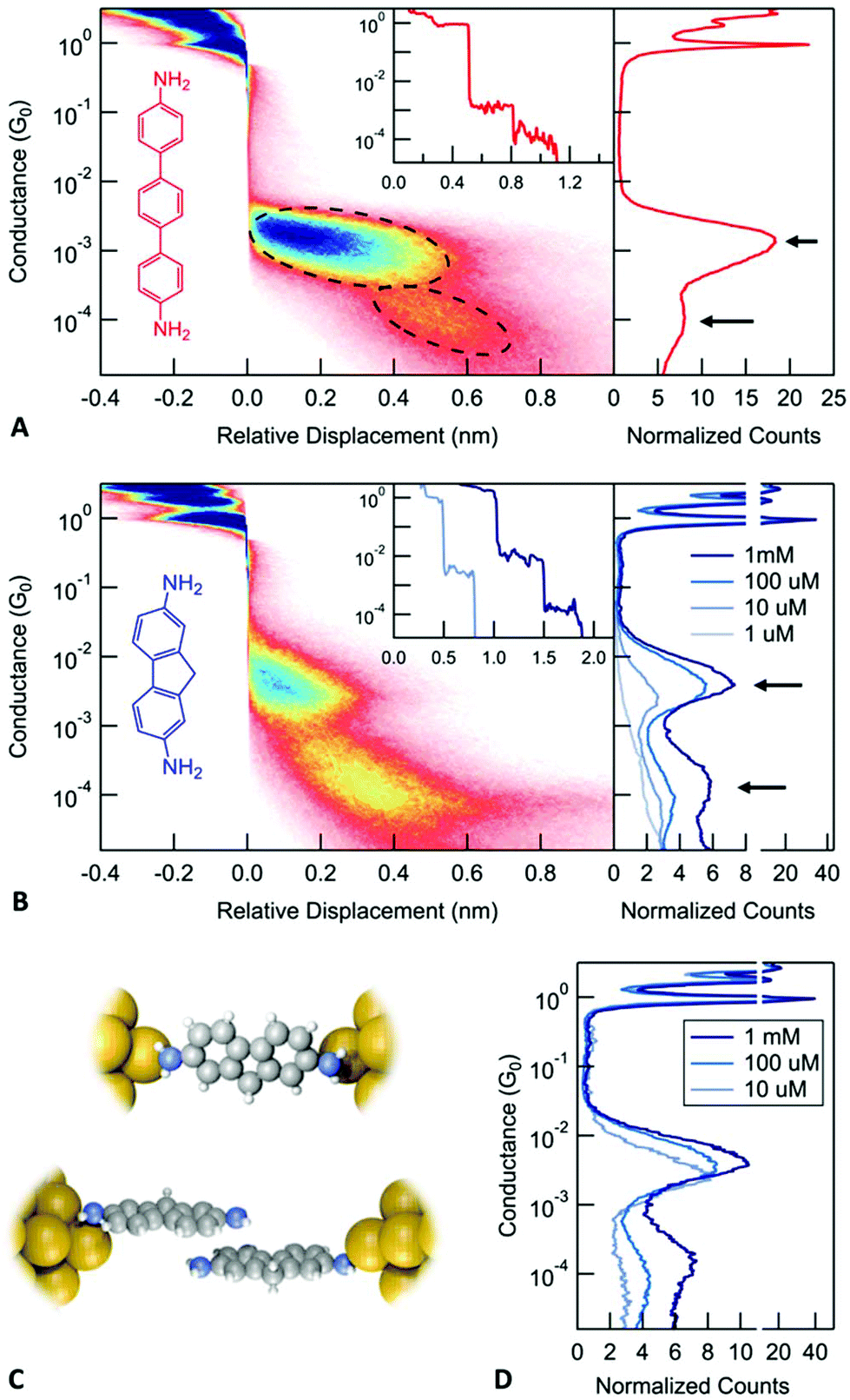 | ||
| Fig. 1 (A) Molecular structure and conductance histograms of 4,4′′-diamino-p-terphenyl (DAT, red). 1D histogram (right panel) exhibits two peaks, indicated by black arrows. The 2D histogram (left panel) displays the evolution of junction conductance during the elongation process. Inset: Sample conductance traces. (B) 1D and 2D histograms for 2,7-diamino fluorene (DAF, blue). The right panel displays histograms measured from 1 μM to 1 mM solutions of DAF in 1,2,4-trichlorobenzene. (C) Illustration of the DAF monomer and dimer junctions. (D) Histogram for the traces that show a conductance plateau longer than 0.15 nm in the range from 10−2G0 to 10−3G0. | ||
To determine the conductance of a molecular junction from the large datasets collected in these measurements, one dimensional (1D) conductance histograms are generated from all the recorded traces without any data selection. These histograms show peaks at conductance values corresponding to junctions that can sustain a relatively constant conductance upon elongation. The peak positions can be used to identify the conductance of the most frequently occurring junction configuration. The right panel in Fig. 1A and B shows 1D histograms for DAT and DAF, respectively (and ESI-Fig. S1A† shows 1D histograms for 4,4′-diaminostilbene). These conductance histograms are created using logarithmic bins. Both molecules exhibit two peaks in the 1D conductance histograms as indicated by arrows that are separated by roughly a factor of 10. Based on a series of measurements with diamine molecules and the correlation of the measured conductances with calculations,16 we associate the higher conductance with a junction configuration where a molecule is bound with dative Au–N bonds to undercoordinated gold atoms on the two electrodes. We hypothesize that the lower conductance corresponds to a junction where one molecule is bound to each electrode and the two molecules are coupled through a molecule-molecule interaction (see Fig. 1D). We will refer to these configurations as a monomer junction or a dimer junction. In this paper, we provide definitive evidence for this hypothesis and investigate the properties of the stacked dimer junctions.
We first gain some information on the junction elongation process through creating two-dimensional (2D) histograms by aligning all measured traces to have zero displacement at a preset conductance of 0.5G0. Using these histograms, we can obtain information on the relative distance between the gold contact rupture point and any other feature in the junction evolution process. Specifically, from the 2D histograms shown in Fig. 1A for DAT (Fig. 1B for DAF and ESI-Fig. S1A† for 4,4′-diaminostilbene), we note that the lower conducting junction is visible at larger electrode separations when compared with the higher conducting junctions. This is consistent with the following junction evolution process: the metallic contact is ruptured and a monomer junction is first formed. As this junction is elongated, the molecule detaches from one electrode and couples through its pi system to another molecule, which is bound to the other electrode as illustrated in Fig. 1C. Such a dimer junction is able to span a distance between the electrodes that is larger than the length of a single molecule. These features therefore indicate the presence of a stable junction that is longer than a monomer junction. We note that to properly interpret distances from a 2D histogram, one must consider that after the rupture of the metal contact, the gold electrodes snap back opening up a gap between the electrodes that is around 0.6–0.8 nm.17 Therefore, the actual separation between the electrodes is larger than the displacement relative to the rupture of the metallic contact displayed on the 2D histogram. The three molecules measured here show a lower conductance feature at an electrode separation that is comparable to the length of the molecule (the N–N distance is 1.4 nm for DAT and 1.0 nm for DAF), but not significantly longer when the lengths of the N–Au bonds are taken into account as well. Therefore, 2D conductance histograms alone does not provide evidence on the formation of dimer junctions, a more complex investigation is required to support our hypothesis.
If the lower conducting configuration corresponds to dimer junctions, then we should see that the probability to form such junctions depends on the number of molecules available at the surface of the electrodes. We therefore carry out measurements by varying the concentration of the DAF molecular solutions from 1 μM concentration to 1 mM to see how the lower conductance peak evolves (right panel in Fig. 1B). Measurements with a 10 μM solution do not show a clear dimer peak. The dimer peak appears at 100 μM concentration and becomes significantly larger at 1 mM. In order to compare the relative height of these peaks, we created conditional histograms by selecting traces that exhibit a plateau in the conductance region of the monomer (Fig. 1D).18 These clearly show that the ratio of the dimer/monomer peak heights increases with the concentration. Based on these results, we conclude that it is more likely to observe dimer junctions at higher concentration, which is consistent with our hypothesis.
To test the importance of the pi-system in the formation of dimer junctions, we compare these results with measurements of diamine-terminated alkanes. ESI-Fig. S1B† shows the conductance histogram for 1,7-diaminoheptane. A close examination reveals two conductance peaks; however, these are roughly a factor of 2 apart and are due to the formation of molecular junctions with either one or two molecules. Note that the 2D histogram shows that both of these features start right after the rupture of the metal contact in contrast to the results for the conjugated diamines.
Next, we consider the impact of the amine group in forming these dimer junctions by measuring a mono-amine terminated stilbene (4-amino-stilbene).19 We find that the 2D conductance histogram for this molecule (ESI-Fig. 1C†) shows a single molecular feature with an extension that is consistent with the molecular backbone length. Furthermore, the conductance of the molecular junction is not very well defined. We see that the conductance decreases by more than one order of magnitude as the junction is elongated. This has been attributed previously to the formation of a junction that is coupled through a linker-metal bond on one side and a pi-metal interaction on the other.19 We can therefore conclude that the dimer junction does not form with conjugated mono-amines. The pi-orbitals alone do not provide a sufficiently strong coupling to create stable dimer junctions at room temperature with gold electrodes, although this has been observed with platinum electrodes.20,21 As an additional control, we also consider junctions formed with thiochroman linkers (see ESI-Fig. S1D†). We do not observe a signature of the dimer junction in 2D conductance histograms and thus conclude that the N–pi interaction is critical in our observations here.
The attractive interaction between conjugated molecules, also known as pi-stacking, occurs in a geometry where the molecules are laterally offset to allow pi electrons to interact with the positive nuclear cores of carbon atoms.11 In the case of amine terminated aromatic molecules, there are different motifs that could be used to rationalize the interactions between dimers. First, the lone pair on the nitrogen atom can interact with the center of the carbon ring. For example, the crystal structure of a form of 4,4′-biphenyldiamine has the nitrogen atom on one molecule approximately centered above the carbon ring of another molecule.22,23 In addition, van der Waals corrected DFT calculations for 1,4-benzenediamine on the graphite substrate show that there is an energy minimum position for the N atom approximately centered above one carbon ring with a binding energy on the order of 0.5 eV.24 We can therefore expect a similar binding energy for dimers formed in situ in our experiments with DAT and DAF. Second, there can be a hydrogen-bonding interaction between the amino groups in the dimers. Such an interaction has been found in aromatic diamines.25 Although such a molecule–molecule interaction would not be fully consistent with the conductance plateau length observed in the experiments, such a motif has been shown to have a strong electronic coupling, and could therefore play a role in stabilizing a dimer upon junction elongation.26,27 Finally, we could also consider a direct amine-aromatic edge coupling which has been observed in other diamine-based aromatic compounds.25 However, although such a dimer junction structure is hard to rationalize given the conductance versus distance data, we cannot completely rule it out.
We now discuss additional measurements that provide further evidence for the existence of dimer junctions formed by DAT and DAF molecules. Current noise is often measured to gather more information on the junction structure and transport characteristics. In the case of metallic point contacts, shot noise is indicative of the number of open conductance channels and the value of their transmission.28–30 More recently, noise measurements were also applied to molecular junctions.31–39 At room temperature, the dominant noise source in a molecular junction originates from the movement of atoms on the metal electrodes which lead to a fluctuation of the molecule-electrode coupling and hence the measured conductance.36 The resulting conductance noise power spectrum shows a 1/fn frequency dependence, this type of noise is often referred to as flicker noise or 1/f noise. Past work has shown that flicker noise measurements can be used to probe the electronic interaction between molecules and metal electrodes.36 The electronic coupling between a molecule and a metal electrode can be characterized as either through-bond or through-space coupling depending on whether the electronic orbitals responsible for charge transfer also participate in the formation of a chemical bond or not.40 It was demonstrated that the relationship between flicker noise power (PSD) and junction conductance (G) follows a power law dependence (PSD ∝ Gn), with the scaling exponent (n) being indicative of the electronic coupling type: n = 1 implies through-bond coupling while n = 2 is characteristic for through-space coupled junctions.36
In the case of a DAT or a DAF monomer junction, both sides of the molecule are coupled through-bond to the metal electrodes, and therefore we expect the scaling exponent describing the relationship between noise power and junction conductance to be close to 1. By contrast, in case of a dimer junction, the molecule–molecule coupling should include a through-space component and therefore we expect the scaling exponent to increase. To gain better understanding of how the scaling exponent changes in case of dimer junctions, we performed a simulation to generate noise based on a model junction as shown in Fig. 2A. We consider two molecules, each molecule bound to an electrode on one side, with coupling strength ΓL and ΓR, respectively, and with an inter-molecular coupling δ. The conductance of such a model junction can be calculated using a tight-binding method.41 In the limit that δ is much smaller than ΓL and ΓR and when transport is in the off-resonant regime, with the molecular frontier levels being far from the electrode Fermi level, the conductance can be approximated as:
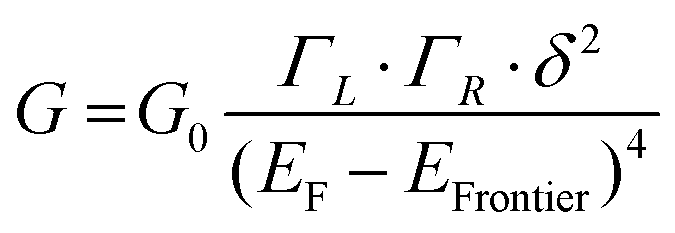
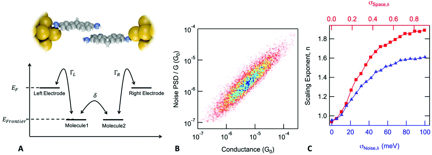 | ||
Fig. 2 Flicker noise characteristics in dimer junctions. (A) Schematics of the model used for calculating conductance of dimer junctions. (B) Two-dimensional histogram created from normalized noise power and average conductance values calculated for 10![[thin space (1/6-em)]](https://www.rsc.org/images/entities/char_2009.gif) 000 simulated traces, parameters were set as: σSpace,δ = 0.6 and σNoise,δ = 20 me V. (C) Red squares: scaling exponent versus σSpace,δ with σNoise,δ fixed to zero. Blue triangles: scaling exponent versus σNoise,δ with σSpace,δ fixed to zero. The scaling exponent is between 1 and 2 depending on the value of these two parameters. In the limit, when both parameters are close to the zero (no junction to junction variance and no noise introduced at the inter-molecular interface) the model is equivalent to a monomer junction with through-bond coupling on both sides. If either of these parameters is changed, scaling exponent increases, therefore we expect the scaling exponent to be close to 2 in case of our experiments with dimer junctions. 000 simulated traces, parameters were set as: σSpace,δ = 0.6 and σNoise,δ = 20 me V. (C) Red squares: scaling exponent versus σSpace,δ with σNoise,δ fixed to zero. Blue triangles: scaling exponent versus σNoise,δ with σSpace,δ fixed to zero. The scaling exponent is between 1 and 2 depending on the value of these two parameters. In the limit, when both parameters are close to the zero (no junction to junction variance and no noise introduced at the inter-molecular interface) the model is equivalent to a monomer junction with through-bond coupling on both sides. If either of these parameters is changed, scaling exponent increases, therefore we expect the scaling exponent to be close to 2 in case of our experiments with dimer junctions. | ||
Using a Monte Carlo simulation, we generate conductance traces and analyze the relationship between noise power and conductance to determine the scaling exponent. Details of the method are described in the ESI.† We assume that conductance noise originates from the fluctuations in the coupling strength parameters: ΓL, ΓR and δ. These parameters have both junction to junction variation and dynamic fluctuations. In case of a through-bond coupled electrode and a molecule, coupling strength is influenced by the atomic arrangement of the electrode in the close vicinity of the metal atom to which the molecule is bound to. We hypothesize that fluctuations of the coupling strength are dominated by the movement of the electrode atoms near the atom connecting the molecule. Therefore, we expect that the fluctuations are independent of the average coupling strength. In case of through-space coupling, the coupling strength is proportional to the overlap between the exponentially decaying wavefunctions of the coupled sites. As a result, coupling strength shows an exponential dependence on the separation between the coupled sites.
In Fig. 2B, we create a histogram of the simulated normalized noise power spectrum density (PSD/G) by against the conductance (G) where we see a clear correlation between the normalized noise and conductance. Through these simulations, we find that this correlation depends on two parameters: σSpace,δ, which describes the junction to junction variation of the inter-molecular coupling strength and σNoise,δ which describes the dynamic fluctuations in δ at the inter-molecular interface within a junction. The scaling exponent, n, that describes the correlation between noise power and conductance (PSD ∝ Gn), is 1.84 for the simulation presented in Fig. 2B but in general, it depends on the value of σSpace,δ and σNoise,δ as shown in Fig. 2C. In the limit when the inter-molecular coupling strength has no junction to junction variation (σSpace,δ = 0) and no dynamic fluctuations (σNoise,δ = 0), we get back the case of a monomer junction with through-bond coupling on both sides. The scaling exponent is then close to 1. Based on these simulations, we conclude that a scaling exponent close to 2 is indicative of a dimer junction with the through-space inter-molecular coupling.
Measurements of junction flicker noise are performed as described previously.36 Briefly, we hold the junction by pausing the elongation process for 150 ms and record the conductance of the junction (sample trace shown in Fig. 3A). We select only those traces, for which the conductance measured at the beginning and end of the hold period is comparable. For each of these traces, two quantities are calculated from the measured conductance while the junction is held: the average conductance (G) and the normalized noise power (PSD/G). The PSD is obtained from an integral of the discrete Fourier transform of the measured conductance between 100 Hz to 1000 Hz. The lower frequency limit is constrained by the mechanical stability of the setup. The upper limit is determined by the input noise of the current amplifier. We note here that the flicker noise measured with molecular junctions at 1000 Hz is still 3 orders of magnitude larger than noise measured on a 10 MΩ resistor using the same experimental setup (ESI-Fig. S2†).
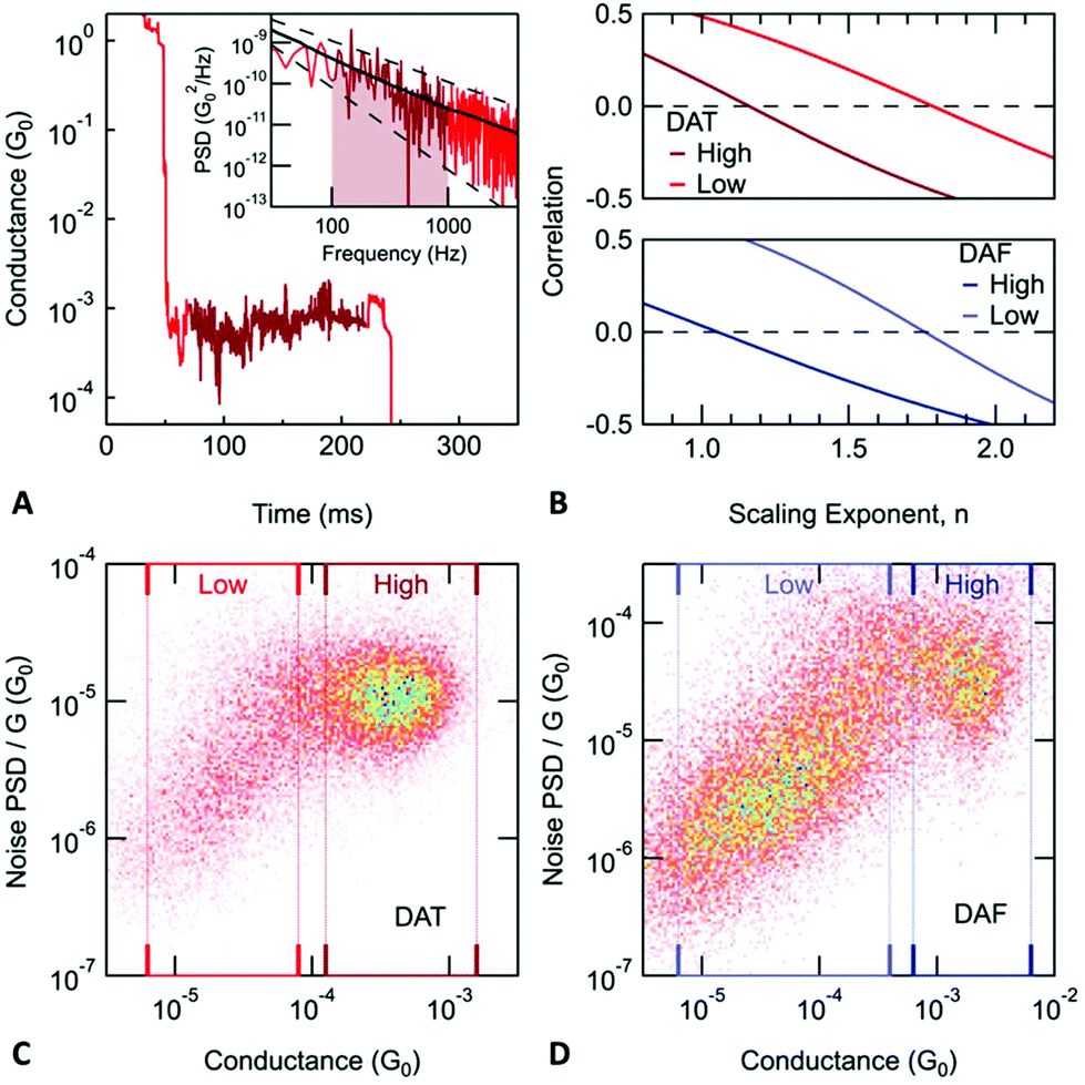 | ||
| Fig. 3 (A) Sample conductance versus time trace for DAT. During the elongation of the junction, the piezo movement is paused for 150 ms. The inset shows the noise power calculated from the conductance measured during the hold period (dark red region). The noise power averaged for all monomer DAT junctions is plotted with a black line. Dashed lines indicate 1/f and 1/f2 frequency dependence. (B) Correlation between average conductance (G) and noise power normalized with Gn. In order to determine the scaling exponent describing the relationship between flicker noise power and average conductance, we take the value of n, where PSD/Gn is independent of G, or equivalently, when the correlation is zero. (C) and (D) Noise power normalized by the average conductance versus the average conductance. Conductance regions corresponding to monomer and dimer junctions are indicated with dark and light rectangles respectively. The exponents describing the relationship between flicker noise and conductance are as follows. Monomer junctions: 1.16 for DAT and 1.05 for DAF. Dimer junctions: 1.78 in the case of DAT and 1.76 for DAF. The estimated error of these scaling exponents is less than 0.02 in all cases. | ||
Using the values of average conductance and noise power obtained for each trace, we create 2D histograms as shown in Fig. 3C and D. The relationship between noise power and conductance is extracted by calculating the Pearson's correlation coefficient between PSD/Gn and G, then determining n such that these two variables are uncorrelated (correlation coefficient is zero) as shown in Fig. 3B. For monomer junctions of DAT and DAF, n is 1.16 and 1.05, respectively, while for the dimer junctions, n is 1.78 and 1.76, respectively. The dimer junctions show a noise characteristic of a through-space coupling while the monomer junctions are coupled through-bond. This is a result based on two independent measured quantities (conductance and noise), which confirms the hypothesis of dimer formation.
To gain more information about the structure and evolution of these junctions, we performed AFM-BJ measurements on DAF and DAT molecules. We measure conductance and force simultaneously during the elongation and rupture of the junctions, using a custom built AFM.13 We use the measured conductance to identify the different junction structures such as metallic point-contact, monomer or dimer junctions. We then analyze the measured force signal to determine and compare mechanical properties of these junctions.
A typical conductance and force trace is shown in Fig. 4A: during the elongation of a stable Au contact, the measured force increases linearly as the junction is elastically deformed until the atoms of the electrode rearrange causing a sudden force drop. These repeated load and rupture events result in a saw-tooth shaped pattern in the measured force signal. In the case of a molecular junction, there are usually multiple load and rupture events present, which are generally attributed to the linkers changing the attachment position on the electrodes.42 The last loading event before the rupture of the molecular junction corresponds to a junction, where the molecule bridges the largest gap between the electrodes and is being stretched as the electrodes are further separated. We observe that even in the case of the dimer junctions, the measured force does not go continuously to noise, instead, a clear force loading is visible before the dimer rupture of the junction. Based on the conductance measurements presented above, we know that the amine group is needed to form these junctions. We therefore hypothesize that the geometry of the dimer has the amine group of one molecule centered above the carbon ring of the other as illustrated in Fig. 1C.
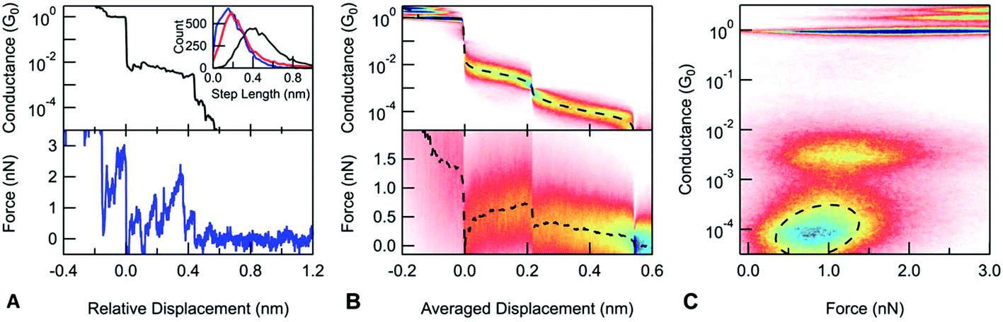 | ||
| Fig. 4 Force spectroscopy measurement on the DAF molecule. (A) Sample conductance and force trace. The inset shows the length distributions: entire molecular step (black), the monomer (blue) and dimer (red) junctions. (B) Scaled conductance (upper) and force (lower) histograms. (C) Conductance versus force histogram. The region of the dimer is fitted with 2D Gaussian with contours of the fit showing a positive correlation of 0.31 between conductance and force. | ||
Next, we explore the rupture force of the stacked dimers by examining the force necessary to rupture the monomer and dimer junctions. We define the rupture force as the difference between the force acting on the junction when it ruptures and the force measured after the final rupture event, when there are no mechanical connections between the sample and tip. Force-displacement 2D histograms have been used to determine junction rupture forces;13 these show how the measured force signal changes on average at the close vicinity of a given point along the trace. When aligned at the junction rupture, the resulting average force curve captures the post rupture drop in the force signal; however, it does not allow us to readily compare the rupture force of different events on a single trace (see the ESI† for more details). To overcome this problem, we construct a new type of scaled 2D force histogram where we align the monomer and dimer rupture at different points along the horizontal axis and overlay data from all measurements. Since the horizontal axis is scaled, the relative displacement information is lost but force information is retained throughout the rupture process. The resulting average force curve shows how the measured force changes during the extension of the junction. We scale each molecular plateau to have an average displacement as determined from an analysis of plateau lengths and use this value to scale the 2D force histogram. Using such a scaled force 2D histogram, the rupture force for both the monomer and the dimer junctions can be determined by simply evaluating the average force curve at the point where the corresponding molecular junction ruptures. In the case of the DAF, the monomer junctions break at 0.72 nN. The dimer junctions break at a significantly lower force of 0.12 nN. Similarly, for DAT (ESI-Fig. S5B†), there is a significant difference between the rupture force of the monomer (0.43 nN) and dimer junctions (0.05 nN). In principle, a dimer junction can either rupture at a molecule-gold bond on one electrode or at the molecule–molecule interface. This significant difference in their rupture forces indicates that the dimer junctions rupture at the molecule–molecule bond.
A closer examination of the scaled conductance and the force histogram reveals that during the elongation of the dimer junctions, both the average conductance and force are decreasing. This is even more visible on a 2D conductance versus the force histogram obtained by simply plotting the conductance data against force data for each trace and overlaying the resulting curves (Fig. 4C).43,44 In the region of the dimer junction, there is a tilted feature indicating a positive correlation between conductance and force. We identify this as a characteristic property of dimer junctions. We expect that both conductance and force depend largely on the extent of the overlap at the molecule–molecule interface which yields a correlated conductance and force signals. In contrast to measurements with DAT and DAF, conductance and force are uncorrelated for a control molecule, 4,4′-bipyridine, as shown in ESI-Fig. 6.†
To conclude, we have investigated the formation of stacked dimers in break junction measurements and compared their electronic and mechanical characteristics with monomer junctions. The probability to form dimer junctions increases with increasing molecular concentration. Based on conductance measurements on a series of molecules, we find that the amine linkers play an important role in mechanically stabilizing the dimer junctions. Through flicker noise measurements, we find that the dimer junctions are electronically coupled through-space. Force measurements show that a significantly smaller force is required to rupture the dimer junction when compared with the monomer junction, consistent with a weak N–pi interaction when compared with an Au–N donor acceptor bond. Finally, we show that for these dimer junctions, conductance and force decrease as the junction is elongated, which shows that the extent of the overlap between the two molecules dictates both the electronic and mechanical characteristics of dimers.
Conflicts of interest
There are no conflicts to declare.Acknowledgements
This work was supported in part by the National Science Foundation under grant DMR-1507440. A. H. and A. M thank the National Research, Development and Innovation Office for support under grant K119797. A. M. also thanks the Fulbright Foundation for support.References
- G. D. Scholes and G. Rumbles, Nat. Mater., 2006, 5(9), 683–696 CrossRef CAS PubMed
.
- T. Nakano, Polym. J., 2010, 42(2), 103–123 CrossRef CAS
- S. Burattini, B. W. Greenland, D. H. Merino, W. Weng, J. Seppala, H. M. Colquhoun, W. Hayes, M. E. Mackay, I. W. Hamley and S. J. Rowan, J. Am. Chem. Soc., 2010, 132(34), 12051–12058 CrossRef CAS PubMed
- S. M. Wu, M. T. Gonzalez, R. Huber, S. Grunder, M. Mayor, C. Schonenberger and M. Calame, Nat. Nanotechnol., 2008, 3(9), 569–574 CrossRef CAS PubMed
- L. Li-Li, S. Xiu-Neng, L. Yi and W. Chuan-Kui, J. Phys.: Condens. Matter, 2010, 22(32), 325102 CrossRef PubMed
- S. Martin, I. Grace, M. R. Bryce, C. S. Wang, R. Jitchati, A. S. Batsanov, S. J. Higgins, C. J. Lambert and R. J. Nichols, J. Am. Chem. Soc., 2010, 132(26), 9157–9164 CrossRef CAS PubMed
- W. Hong, H. Valkenier, G. Mészáros, D. Z. Manrique, A. Mishchenko, A. Putz, P. M. García, C. J. Lambert, J. C. Hummelen and T. Wandlowski, Beilstein J. Nanotechnol., 2011, 2, 699–713 CrossRef PubMed
- M. T. González, E. Leary, R. García, P. Verma, M. Á Herranz, G. Rubio-Bollinger, N. Martín and N. Agraït, J. Phys. Chem. C, 2011, 115(36), 17973–17978 Search PubMed
- K. Yoshida, I. V. Pobelov, D. Z. Manrique, T. Pope, G. Mészáros, M. Gulcur, M. R. Bryce, C. J. Lambert and T. Wandlowski, Sci. Rep., 2015, 5, 9002 CrossRef CAS PubMed
- J.-T. Zheng, R.-W. Yan, J.-H. Tian, J.-Y. Liu, L.-Q. Pei, D.-Y. Wu, K. Dai, Y. Yang, S. Jin, W. Hong and Z.-Q. Tian, Electrochim. Acta, 2016, 200, 268–275 CrossRef CAS
- B. Q. Xu and N. J. Tao, Science, 2003, 301(5637), 1221–1223 CrossRef CAS PubMed
- B. Q. Xu, X. Y. Xiao and N. J. Tao, J. Am. Chem. Soc., 2003, 125(52), 16164–16165 CrossRef CAS PubMed
- M. Frei, S. V. Aradhya, M. Koentopp, M. S. Hybertsen and L. Venkataraman, Nano Lett., 2011, 11(4), 1518–1523 CrossRef CAS PubMed
- C. Nef, P. L. T. M. Frederix, J. Brunner, C. Schönenberger and M. Calame, Nanotechnology, 2012, 23(36), 365201 CrossRef CAS PubMed
- I. W. P. Chen, W.-H. Tseng, M.-W. Gu, L.-C. Su, C.-H. Hsu, W.-H. Chang and C.-h. Chen, Angew. Chem., Int. Ed., 2013, 52(9), 2449–2453 CrossRef CAS PubMed
- M. S. Hybertsen and L. Venkataraman, Acc. Chem. Res., 2016, 49(3), 452–460 CrossRef CAS PubMed
- A. I. Yanson, G. R. Bollinger, H. E. van den Brom, N. Agrait and J. M. van Ruitenbeek, Nature, 1998, 395(6704), 783–785 CrossRef CAS
- P. Makk, D. Tomaszewski, J. Martinek, Z. Balogh, S. Csonka, M. Wawrzyniak, M. Frei, L. Venkataraman and A. Halbritter, ACS Nano, 2012, 6(4), 3411–3423 CrossRef CAS PubMed
- J. S. Meisner, S. Ahn, S. V. Aradhya, M. Krikorian, R. Parameswaran, M. Steigerwald, L. Venkataraman and C. Nuckolls, J. Am. Chem. Soc., 2012, 134(50), 20440–20445 CrossRef CAS PubMed
- M. Kiguchi, O. Tal, S. Wohlthat, F. Pauly, M. Krieger, D. Djukic, J. C. Cuevas and J. M. van Ruitenbeek, Phys. Rev. Lett., 2008, 101(4), 046801 CrossRef CAS PubMed
- T. Yelin, R. Korytar, N. Sukenik, R. Vardimon, B. Kumar, C. Nuckolls, F. Evers and O. Tal, Nat. Mater., 2016, 15(4), 444–449 CrossRef CAS PubMed
- M. Rafilovich and J. Bernstein, J. Am. Chem. Soc., 2006, 128(37), 12185–12191 CrossRef CAS PubMed
- X. Chen, B. Ma, X. Wang, S. Yao, L. Ni, Z. Zhou, Y. Li, W. Huang, J. Ma, J. Zuo and X. Wang, Chemistry, 2012, 18(37), 11828–11836 CrossRef CAS PubMed
- T. Kim, Z. F. Liu, C. Lee, J. B. Neaton and L. Venkataraman, Proc. Natl. Acad. Sci. U. S. A., 2014, 111(30), 10928–10932 CrossRef CAS PubMed
- A. L. Llamas-Saiz, C. Foces-Foces, P. Molina, M. Alajarin, A. Vidal, R. M. Claramunt and J. Elguero, J. Chem. Soc., Perkin Trans. 2, 1991,(7), 1025–1031 RSC
- G. Balducci, M. Romeo, M. Stener, G. Fronzoni, D. Cvetko, A. Cossaro, M. Dell'Angela, G. Kladnik, L. Venkataraman and A. Morgante, J. Phys. Chem. C, 2015, 119(4), 1988–1995 CAS
- G. Kladnik, D. Cvetko, A. Batra, M. Dell'Angela, A. Cossaro, M. Kamenetska, L. Venkataraman and A. Morgante, J. Phys. Chem. C, 2013, 117(32), 16477–16482 CAS
- H. E. van den Brom and J. M. van Ruitenbeek, Phys. Rev. Lett., 1999, 82(7), 1526–1529 CrossRef CAS
- B. Ludoph and J. M. van Ruitenbeek, Phys. Rev. B: Condens. Matter Mater. Phys., 2000, 61(3), 2273–2285 CrossRef CAS
- M. Kumar, K. K. V. Sethu and J. M. van Ruitenbeek, Phys. Rev. B: Condens. Matter Mater. Phys., 2015, 91(24), 245404 CrossRef
- R. Ochs, D. Secker, M. Elbing, M. Mayor and H. B. Weber, Faraday Discuss., 2006, 131, 281–289 RSC
- D. Djukic and J. M. van Ruitenbeek, Nano Lett., 2006, 6(4), 789–793 CrossRef CAS PubMed
- O. Tal, M. Krieger, B. Leerink and J. M. van Ruitenbeek, Phys. Rev. Lett., 2008, 100(19), 196804 CrossRef CAS PubMed
- M. Tsutsui, M. Taniguchi and T. Kawai, Nat. Commun., 2010, 1, 138 CrossRef PubMed
- D. Xiang, T. Lee, Y. Kim, T. Mei and Q. Wang, Nanoscale, 2014, 6(22), 13396–13401 RSC
- O. Adak, E. Rosenthal, J. Meisner, E. F. Andrade, A. N. Pasupathy, C. Nuckolls, M. S. Hybertsen and L. Venkataraman, Nano Lett., 2015, 15(6), 4143–4149 CrossRef CAS PubMed
- D. Xiang, V. Sydoruk, S. Vitusevich, M. V. Petrychuk, A. Offenhäusser, V. A. Kochelap, A. E. Belyaev and D. Mayer, Appl. Phys. Lett., 2015, 106(6), 063702 CrossRef
- M. A. Karimi, S. G. Bahoosh, M. Herz, R. Hayakawa, F. Pauly and E. Scheer, Nano Lett., 2016, 16(3), 1803–1807 CrossRef CAS PubMed
- D. Cho, H. Lee, S. Shekhar, M. Yang, J. Y. Park and S. Hong, Sci. Rep., 2017, 7, 43411 CrossRef CAS PubMed
- R. Hoffmann, Acc. Chem. Res., 1971, 4(1), 1–9 CrossRef CAS
- J. R. Widawsky, W. Chen, H. Vazquez, T. Kim, R. Breslow, M. S. Hybertsen and L. Venkataraman, Nano Lett., 2013, 13(6), 2889–2894 CrossRef CAS PubMed
- S. V. Aradhya, M. Frei, M. S. Hybertsen and L. Venkataraman, Nat. Mater., 2012, 11(10), 872–876 CrossRef CAS PubMed
- K. Wang, J. M. Hamill, J. Zhou and B. Xu, J. Am. Chem. Soc., 2014, 136(50), 17406–17409 CrossRef CAS PubMed
- J. M. Hamill, K. Wang and B. Xu, Nanoscale, 2014, 6(11), 5657–5661 RSC
Footnote |
| † Electronic supplementary information (ESI) available. See DOI: 10.1039/c7nr08354h |
| This journal is © The Royal Society of Chemistry 2018 |