
 Open Access Article
 This Open Access Article is licensed under a
 Creative Commons Attribution 3.0 Unported Licence
Repeated roll-to-roll transfer of two-dimensional materials by electrochemical delamination†
M.
Hempel
 *a,
A.-Y.
Lu
a,
F.
Hui
b,
T.
Kpulun
c,
M.
Lanza
b,
G.
Harris
c,
T.
Palacios
a and
J.
Kong
a
*a,
A.-Y.
Lu
a,
F.
Hui
b,
T.
Kpulun
c,
M.
Lanza
b,
G.
Harris
c,
T.
Palacios
a and
J.
Kong
a
aDepartment of Electrical Engineering and Computer Science, Massachusetts Institute of Technology, 77 Massachusetts Avenue, Cambridge, Massachusetts 02139, USA. E-mail: marekh@mit.edu
bInstitute of Functional Nano and Soft Materials (FUNSOM), Collaborative Innovation Center of Suzhou Nanoscience and Technology, Soochow University, Suzhou, China
cDepartment of Electrical and Computer Engineering, Howard University, Washington, DC 20059, USA
First published on 12th February 2018
Abstract
Two-dimensional (2D) materials such as graphene (Gr), molybdenum disulfide and hexagonal boron nitride (hBN) hold great promise for low-cost and ubiquitous electronics for flexible displays, solar cells or smart sensors. To implement this vision, scalable production, transfer and patterning technologies of 2D materials are needed. Recently, roll-to-roll (R2R) processing, a technique that is widely used in industry and known to be cost-effective and scalable, was applied to continuously grow and transfer graphene. However, more work is needed to understand the possibilities and limitations of this technology to make R2R processing of 2D materials feasible. In this work, we fabricated a custom R2R transferring system that allows the accurate control of the process parameters. We employ continuous electrochemical delamination, known as “bubble transfer”, to eliminate chemical etchant waste and enable the continuous transfer of 2D materials from metal foils. This also makes our transfer method a renewable and environmentally friendly process. We investigate the surface topology as well as the electrical parameters of roll-to-roll transferred graphene on polyethylene terephthalate (PET) coated with ethylene-vinyl acetate (EVA). Furthermore, we demonstrate for the first time the stacking of two layers of graphene or graphene on hBN by repeated lamination and delamination onto EVA/PET. These results are an important contribution to creating low-cost, large scale and flexible electronics based on 2D materials.
Introduction
Two-dimensional (2D) materials such as graphene (Gr), molybdenum disulfide (MoS2) and hexagonal boron nitride (hBN) exhibit a wide variety of electronic properties, including metallic, semiconducting and insulating behavior. This allows their combination to build up electronic devices entirely made of 2D materials, such as field effect transistors,1 memristors2 and sensors.3 Furthermore, 2D materials are transparent, flexible and mechanically robust, which makes them ideal for building flexible and optoelectronic applications such as wearable electronics,4–6 solar cells7–9 and light-emitting devices.10,11Roll-to-roll (R2R) processing is widely used in the flexible electronics industry to fabricate solar cells, flexible displays and sensors, and has grown to a multi-billion-dollar industry in recent years.12 However, its use in the fabrication of 2D materials is just starting. Two aspects have to be developed to process 2D materials in a roll-to-roll fashion: continuous synthesis and continuous transfer. Continuous synthesis of graphene, the most prominent member of the 2D material family, has been readily demonstrated on Cu foil using chemical vapor deposition.13–15 Although the continuous growth of other 2D materials has not been shown yet, important preliminary steps have been demonstrated thanks to the development of chemical vapor deposition (CVD) growth on metal foils of, for example, MoS2 or WS2 on Au foils,16–18 and hBN on Fe, Cu or Pt foils.19–21
A second important step towards the use of R2R technology in 2D materials is the roll-to-roll transfer onto flexible substrates. The first R2R transfer was reported by Bae et al.22 in 2010 who transferred graphene from a Cu foil onto polyethylene terephthalate (PET) using thermal release tape. Since then, several other groups demonstrated R2R transfers of graphene14,15,23–28 onto flexible substrates using either direct lamination on the target substrate23–28 or epoxy gluing.15 However, these approaches mostly use wet etching of the Cu substrate,14,15,22–25 which is not economical for large-scale production due to the high consumption, and large cost of ultra-pure copper. Furthermore, chemical etching potentially deteriorates the graphene film quality, degrading its electronic properties.29 To circumvent these problems, the electrochemical delamination of graphene and other 2D materials21,30,31 has been shown to gently lift off the 2D layer from the metal foil without the need for chemical etching. This approach reduces waste, allows the metal catalyst to be reused and preserves the material's intrinsic properties. More recently, electrochemical delamination has been integrated in a R2R graphene transfer system27,28 in combination with metal nanowires to achieve a remarkably low sheet resistance of 8 Ω □−1 for transparent electrode applications. However, more work is needed to better understand the factors limiting R2R transfer, such as surface topology and roughness. Furthermore, it is desirable to extend this technique to transfer other 2D materials.
In this work, we study the R2R transfer of graphene and hBN onto plastic substrates by hot roll lamination and electrochemical delamination. To do that, we designed and built an entire transfer system that allows for the fine control of lamination process parameters, including the applied heat and pressure, as well as control of the lamination and delamination speed. Furthermore, we studied the stacking of multiple 2D layers by repeated lamination for the first time.
Experimental details
The 2D material transfer processes reported in this work were carried out using a custom designed R2R system. As shown in Fig. 1(a), the setup consists of three parts: a lamination unit, an electrochemical delamination unit and a rewind unit. The lamination unit is composed of two steel rollers. They are heated by using heat shoes, which can vary the lamination temperature between 80–250 °C. The lamination speed can be altered between 0.7–5 mm s−1 by using a DC motor that actuates the rollers using a gear transmission. Additionally, the force with which the two rollers press together can be adjusted between 0–400 N. The pressure can be changed by compressing the four springs, which push the vertically movable bottom roller up against the clamped-down top roller. The electrochemical delamination unit consists of a stationary Teflon cylinder that is immersed half way into an electrolyte-filled Pyrex glass dish. The delamination process is based on the so-called “bubble transfer” first presented by Wang et al.30 In short, a voltage is applied between the metal foil and a platinum counter electrode that are immersed in the electrolyte. This generates oxygen gas at the platinum electrode, and hydrogen bubbles at the interface of the metal foil and 2D material, which gently separate them. Lastly, the rewind unit is responsible to pick up the delaminated films on separate spools. A typical transfer of 7.5 cm long substrates takes approximately 40 s for the lamination and 60 s for the delamination, which is significantly faster than an etch-based process. Additional parameters and technical details for the transfer setup are provided in the ESI.† | ||
| Fig. 1 (a) Schematic of the R2R transfer setup consisting of a hot roll lamination unit, electrochemical delamination unit and rewind unit. (b) Actual implementation of the transfer setup. (c) Transfer process flow starting with growing the 2D material on a metal film, laminating it in between plastic substrates on top and bottom by applying pressure and heat, electrochemically separating the 2D layers from the metal surface, rinsing the plastic substrates and gluing them on glass slides for further characterization. | ||
A typical transfer process flow is shown in Fig. 1(c). It starts with the synthesis of the 2D material on a metal foil by chemical vapor deposition (Cu for graphene growth or Pt for hBN growth). Next, the 2D-material covered metal foil is laminated on both sides with flexible polymer substrates. The applied heat and pressure of the metal rollers in the lamination unit lightly melt the polymer substrates and bonds them to the 2D material layers. Subsequently, an electrochemical delamination process in an electrolyte bath is used to separate the 2D layer from the metal surface. This delamination happens continuously as the individual ends of the three films are pulled and rolled up by the rewind unit. After separating the entire strip, the rolled-up flexible substrates are taken off the spools, rinsed under DI water and blow-dried. For the purpose of evaluating the transfer quality, they are glued onto glass slides and cut into 1 × 1 cm2 squares for further electrical or material characterization. More details about the lamination and delamination process as well as a video of the transfer process are given in the ESI.†
Results and discussion
To better understand the R2R transfer process of 2D materials, a typical graphene transfer onto polyethylene terephthalate (PET) coated with ethylene-vinyl acetate (EVA) was characterized at three stages: cleaned copper foil before graphene growth, copper foil after graphene growth and transferred graphene on the EVA/PET target substrate. The samples were analyzed by obtaining scanning electron microscopy (SEM) and atomic force microscopy (AFM) images on the same location of the sample (markers were used) at each stage, which allowed detecting morphology changes. Fig. 2(a) shows the SEM (top) and AFM (bottom) results of a pristine copper foil that was pre-cleaned in the nickel etchant for 90 seconds to remove the native oxide layer. Different copper grains and vertical lines are visible in the SEM image. The lines are typical of metal foils and stem from the production process when the Cu is thinned down. The AFM image also illustrates these deep vertical groves, which create an average surface roughness of 75 nm. After graphene growth, the copper surface smoothens out significantly and the average surface roughness decreases to 23 nm, as shown in the AFM image in Fig. 2(b). The surface becomes wavy and now exhibits steps, which are attributed to the release of strain at the copper surface during the cooling process.32 The SEM image in Fig. 2(b) shows the same copper steps as in the AFM image. It also shows graphene wrinkles that result from the thermal expansion mismatch between Cu and graphene as the sample cools down after growth (at 1000 °C). Next, the Gr/Cu sample was laminated onto an EVA/PET target substrate. Previous reports found that the adhesion energy of graphene to EVA is 0.6 J m−2,42 which is slightly lower than the adhesion energy of graphene to copper with 0.72 J m−2.41 Hence, an electrochemical delamination process is used to assist the separation of graphene from the copper surface and enable a complete transfer. The AFM image obtained on the graphene/EVA/PET sample, displayed in Fig. 2(c), indicates that the waviness of the copper substrate was imprinted onto the EVA surface and identical copper steps can be found. This exact negative replication is not surprising because the EVA film melts during the lamination above 120 °C and is hence able to be molded easily. Also, the SEM image in Fig. 2(c) shows identical graphene wrinkles compared to Fig. 2(b) which confirms the exact transfer and good adhesion of graphene to the EVA/PET film (both images in Fig. 2(c) were mirrored to enable an easier comparison). Lastly, the SEM image in Fig. 2(c) reveals local defects in the graphene sheet (that show up as spots with a dark, blurry perimeter due to charging effects). An analysis of typical Gr/EVA/PET SEM images indicates that on average roughly 5% of the transferred area contains cracks or defects (see the ESI† for details).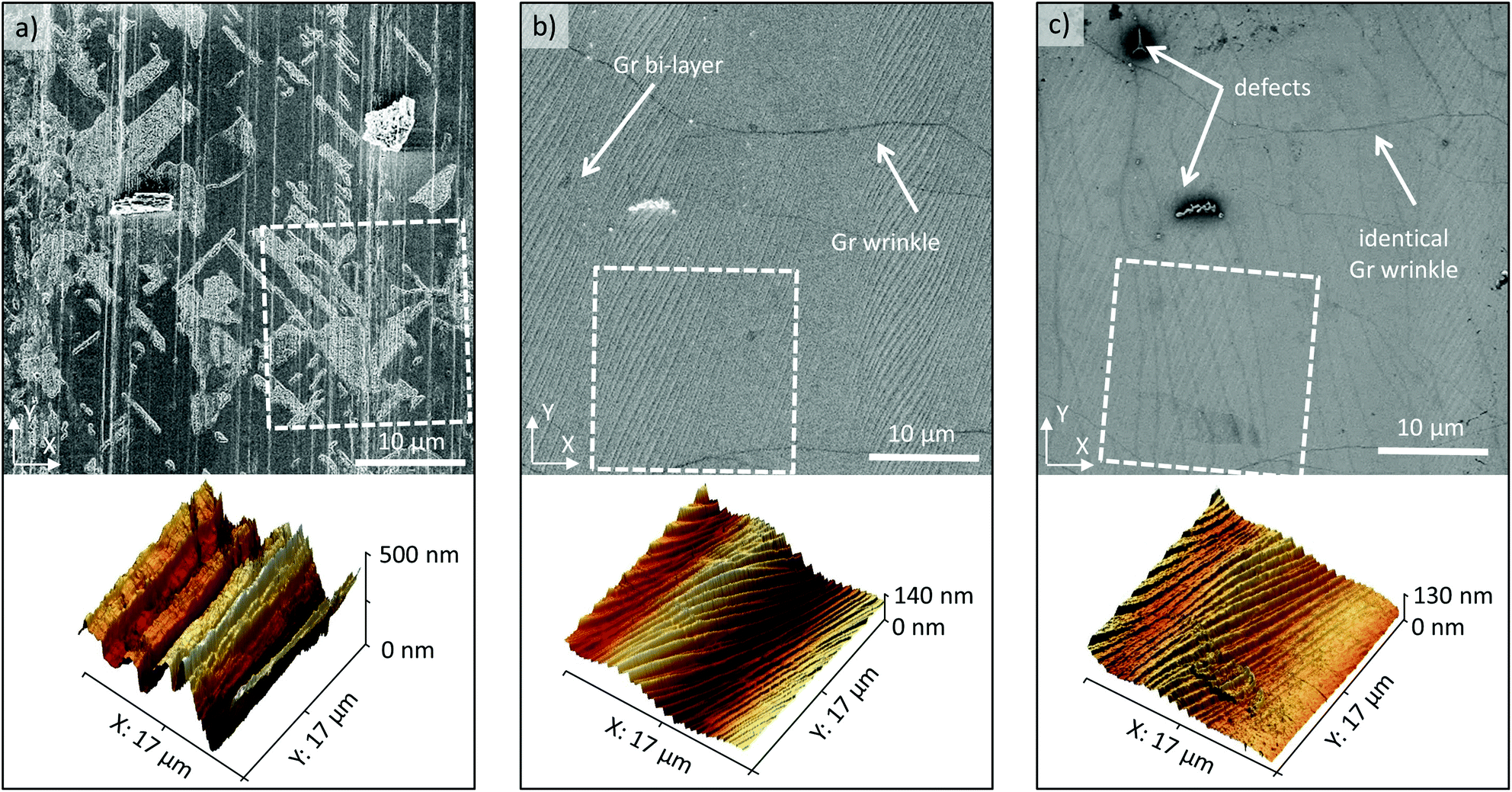 | ||
| Fig. 2 Surface characterization of a graphene transfer process with SEM images at the top and three-dimensional AFM images at the bottom. Areas outlined by white dashed boxes in the SEM images (top) correspond to the regions scanned by AFM (bottom). (a) Surface of copper foil after 90 s nickel etchant cleaning, (b) copper surface after graphene growth, (c) EVA/PET surface after lamination onto copper film and electro-chemical delamination (the SEM in c) was mirrored along the y-axis and AFM image was rotated along the y-axis by 180° for an easier comparison with (b). | ||
Electrical measurements were used to further evaluate the quality of the R2R transferred graphene. In particular, van der Pauw measurements were carried out to determine the sheet resistance Rsh, while Hall effect measurements on the same structures were used to extract the effective carrier concentration ns = (p–n). Given these two values, the carrier mobility μ can be extracted as μ = 1/(q·Rsh·ns). Three sets of samples were measured and analyzed: R2R transferred graphene on EVA/PET (Gr/EVA/PET), as well as two sets of graphene reference samples using a PMMA-assisted wet transfer to SiO2/Si substrates. The first set of reference samples was wet etched in the copper etchant (Gr/SiO2 etched) while the other set was delaminated using electrochemical delamination also known as bubble-transfer (Gr/SiO2 bubble) (see the ESI†). Fig. 3(a) compares the sheet resistance distribution of these samples. The average sheet resistance of the Gr/SiO2 etched reference samples is approximately 500 Ω □−1, with a standard deviation of 57 Ω □−1. Using bubble-transfer to separate the graphene from the Cu substrate, the average sheet resistance of the Gr/SiO2 bubble reference samples is approx. 1200 Ω □−1 with a standard deviation of 189 Ω □−1. Lastly, the R2R transferred Gr/EVA/PET samples have an average sheet resistance of about 4.5 kΩ □−1 with a standard deviation of 960 Ω □−1, which is comparable to the results of graphene on EVA/PET from other groups.23–25,27,28 However, this result also indicates that the R2R transfer process is more variable and results in a much higher sheet resistance as compared to wet transfers on SiO2. To gain more insight into these electrical results, Fig. 3(b) plots the sheet resistance as a function of carrier concentration and carrier mobility. The results show that the Gr/SiO2 etched reference samples have the highest doping concentration and lowest carrier mobility of all samples (avg. ns = 6 × 1012 cm−2 holes, avg. μ = 2727 cm2 V−1 s−1). Changing the delamination method to a bubble transfer lowers the average doping concentration by a factor of three while it slightly increases the carrier mobility (avg. ns = 2 × 1012 cm−2, avg. μ = 2924 cm2 V−1 s−1). This is consistent with previous findings33 showing that an electrochemical transfer introduces less doping compared to etch-based transfers. The reduced doping and defect density, in turn, lower the amount of Coulomb and defect scattering and lead to a higher carrier mobility. The trend of lower doping concentration and higher carrier mobility is most pronounced in the Gr/EVA/PET samples (avg. ns = 3 × 1011 cm−2, avg. μ = 6000 cm2 V−1 s−1). This suggests that the EVA substrate instead of SiO2 further helps to reduce doping and boost the carrier mobility. Such large mobility values of 6000 cm2 V−1 s−1 are relatively high for CVD graphene and typically not achieved on SiO2 substrates. The p-doping behavior that has been observed in all graphene samples likely originates from oxygen doping from the atmosphere.34
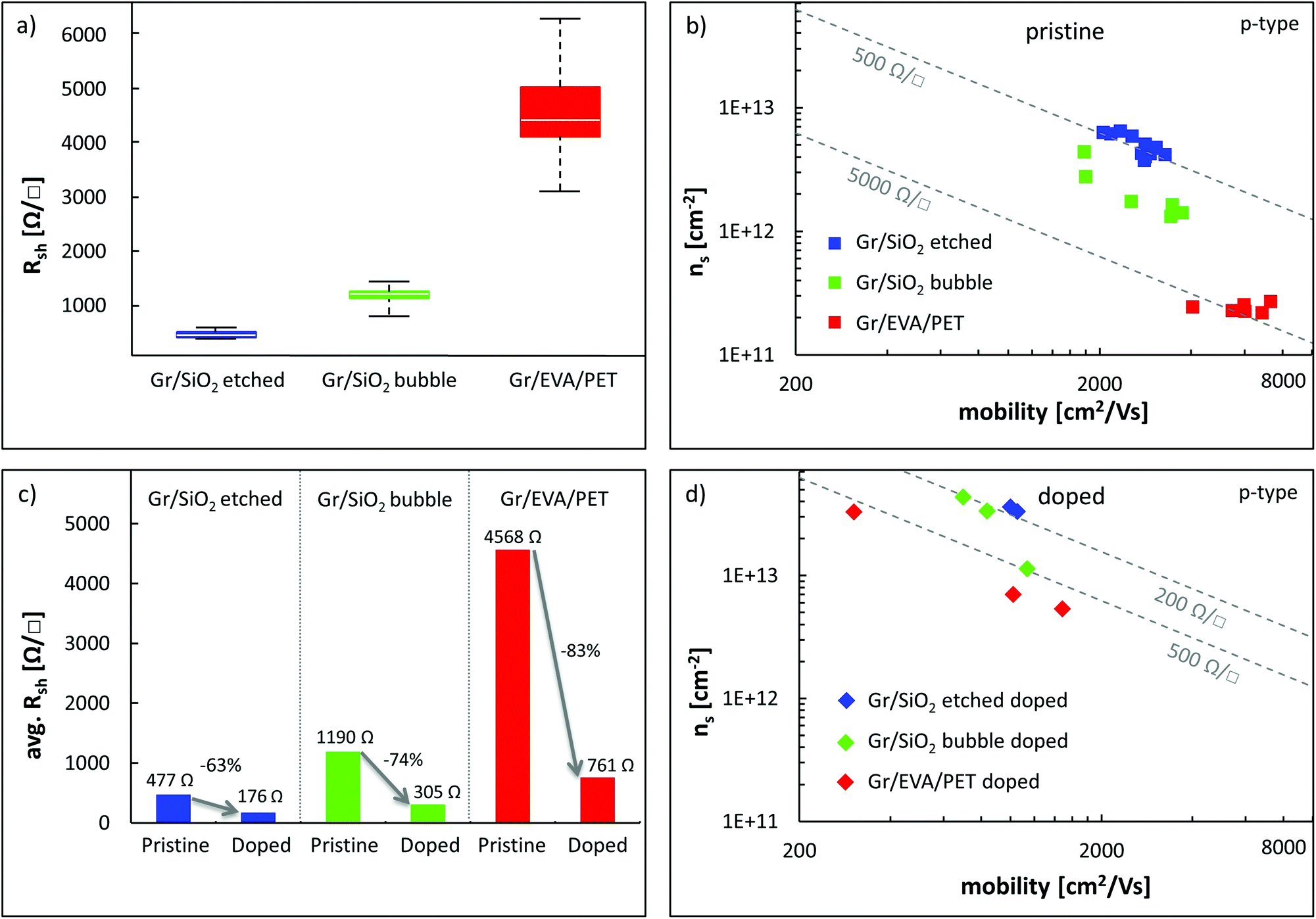 | ||
| Fig. 3 Electrical characterization of Gr/EVA/PET and two sets of reference samples (Gr/SiO2 etched and Gr/SiO2 bubble). (a) Comparison of sheet resistance distribution of Gr/SiO2 etched, Gr/SiO2 bubble and Gr/EVA/PET. (b) Sheet resistance decomposition into Hall mobility and effective carrier concentration of data points in (a). (c) Effects of nitric acid vapor doping on average sheet resistance of Gr/SiO2 etched, Gr/SiO2 bubble and Gr/EVA/PET. (d) Sheet resistance decomposition into Hall mobility and effective carrier concentration of data points in (c). | ||
To test the potential for lowering the graphene sheet resistance, some of the Gr/SiO2 etched, Gr/SiO2 bubble and Gr/EVA/PET samples were doped by exposing them to nitric acid (HNO3) vapor, which produces a temporary doping of the graphene. The results are shown in Fig. 3(c) and (d). After exposure to HNO3, both the reference and Gr/EVA/PET samples are strongly doped, reaching carrier concentrations above 1 × 1013 cm−2 (p-type). The initial high carrier mobility of the R2R samples dropped to below 2000 cm2 V−1 s−1, which is now comparable to the reference samples on silicon dioxide after doping. The lowered carrier mobility of all samples is likely the result of the increased Coulomb scattering, which is caused by the increased doping concentration.37 The results furthermore show that doping the Gr/EVA/PET samples is an effective way to reduce the sheet resistance by over 80% because the relative loss in carrier mobility is smaller than the relative gain in carrier concentration. This approach could ultimately enable graphene for flexible and conductive film optoelectronic applications.
Electrical measurements were also used to test the influence of different lamination temperatures on the quality of the transferred graphene films. Before starting the lamination experiments, the minimum temperature was determined to be 130 °C (see the ESI† for details). To gauge the influence of the lamination temperature, Gr/Cu strips were laminated with 8 different temperatures from 130 °C to 200 °C in 10 °C increments. Subsequently, every sample was delaminated with standard parameters and measured electrically. It was found that the lamination temperature had no discernable impact on sheet resistance. However, the amount of “squeezed out” EVA on the sides increased with increasing temperature. We hypothesize that the exact lamination temperature over 130 °C is not significant because the EVA is always in a molten state and thus always conforms well to the copper topology for any of the tested temperatures. This low melting temperature of EVA, however, is a limiting factor for device fabrication. Building devices on Gr/EVA/PET substrates likely requires processing temperatures below about 80 °C so the EVA adhesive does not melt. However, this problem can be circumvented by integrating the Gr/EVA layer last in a device. This way, flexible solar cells,9 triboelectric generators38 and touch screens39 using Gr/EVA have been demonstrated. The use of PET as a substrate is well suited for flexible electronics due to its mechanical strength and transparency.46
Another way to improve the sheet resistance of Gr/EVA/PET besides chemical doping is by stacking multiple graphene layers. In this work, we demonstrate that two layers of graphene can be stacked by hot roll lamination and electrochemical delamination, which reduces the sheet resistance by 70%. Fig. 4(a) illustrates the process flow. EVA/PET films were laminated on both sides of a graphene-covered Cu strip and delaminated using the standard parameters described before (see the ESI†). Then, the Gr/EVA/PET films were laminated onto a new Cu strip with graphene grown on it and delaminated a second time. Furthermore, mono-layer and bi-layer samples were also subjected to 5 min of nitric acid vapor to dope them. The stacking of multiple graphene layers is more challenging than a simple lamination of graphene onto EVA from an adhesion energy perspective. The binding energy of graphene to graphite is roughly 0.2 J m−2,43,44 which is much less than the adhesion energy of 0.72 J m−2 reported for graphene to copper.41 As a result, the electrochemical delamination process is more important now to offset this difference and facilitate the transfer. The average sheet resistance of one and two layers of graphene on EVA/PET as well as the carrier mobility and concentration (p-type) are shown in Fig. 4(b) and (d), respectively. First of all, Fig. 4(b) shows a sheet resistance reduction by 70% when going from one to two layers. This is surprising because one would expect a roughly doubled carrier concentration and constant carrier mobility which would result in a reduction by approximately 50%22 (assuming no strong interaction between the graphene layers themselves). Fig. 4(d) indicates that this 70% resistance reduction comes partially from an increased carrier mobility (avg. μ1L = 6000 cm2 V−1 s−1versus avg. μ2L = 7600 cm2 V−1 s−1) and a 2.5 times higher carrier concentration (avg. ns,1L = 2.4 × 1011 cm−2versus ns,2L = 6.2 × 1011 cm−2). We believe that this strong sheet resistance decrease may be attributed to cracks and tears in the two graphene layers that are bridged by each other and hence increase the average carrier mobility. Additionally, the larger carrier concentration might be caused by trapped dopants in between the graphene layers. Regarding the effects of chemical doping, Fig. 4(b) shows that the sheet resistance of the bi-layer graphene samples can be lowered even further down to approximately 500 Ω □−1. The carrier mobility and concentration of the doped bi-layers change in a similar way to what was observed for doping monolayer graphene. This time, the sheet resistance improves by roughly 80%, which again is attributed to a strong increase in carrier concentration by over ten times compared to a moderate reduction in carrier mobility due to more Coulomb scattering sites.
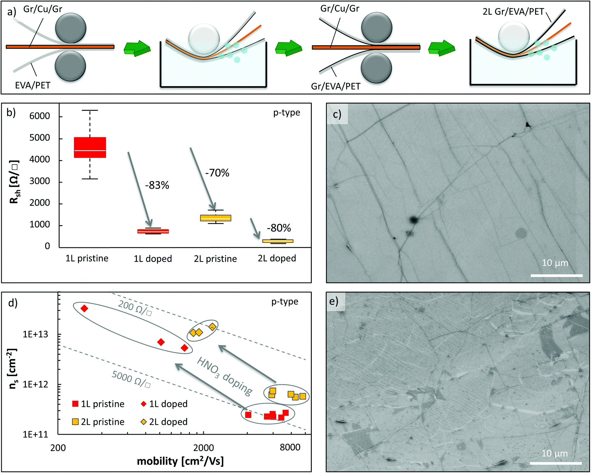 | ||
| Fig. 4 Roll-to-roll transfer of one and two graphene layers. (a) Process flow of transferring two graphene layers by laminating and delaminating twice onto the same substrate. (b) Sheet resistance of one and two layers of graphene on EVA/PET doped and undoped. (c) SEM picture of single graphene layer on EVA/PET. (d) Carrier concentration and mobility of data points from (b). (e) SEM image of two graphene layers on EVA/PET. | ||
For additional characterization, a single and bi-layer sample of graphene on EVA/PET were analyzed by SEM as shown in Fig. 4(c) and (e), respectively. The single graphene layer on EVA/PET looks similar to the one in Fig. 2(c) and shows the typical graphene wrinkles seen as darker lines and a graphene bi-layer island seen as a darker spot. The SEM micrograph of the bi-layer graphene sample, however, shows both white and dark lines as well as dark areas in the image. We believe the white lines to be the tears of the first graphene layer that form when the EVA supporting layer melts and molds to the surface topology of the new copper surface. Both the electrical results and SEM images confirm that the adhesion between graphene and graphene is sufficient for a R2R transfer process.
Finally, the co-lamination of graphene and hexagonal boron nitride (hBN) was investigated. hBN is an insulator and has a hexagonal lattice structure similar to graphene. Recently, graphene films on hBN were demonstrated to have up to three times higher carrier mobility due to less doping from the substrate.20,35 This experiment was designed to first determine if stacking of graphene and hBN by a roll-to-roll transfer is possible and secondly if the beneficial impact of hBN on the mobility of graphene can be maintained. From an adhesion point of view, the binding energy of graphene to hBN was calculated to be approximately −70 meV per unit cell,40 which translates into an adhesion energy of 0.205 J m−2 (see the ESI†). Having a nearly identical value to the adhesion energy of Gr/Gr (0.2 J m−2![[thin space (1/6-em)]](https://www.rsc.org/images/entities/char_2009.gif) 43,44), a successful stacking by R2R transfer seems possible. Before starting the R2R transfers, some samples of hBN were transferred onto silicon pieces with a 300 nm thermal oxide to characterize the material. Fig. 5(a) shows an optical micrograph of hBN on SiO2. It can be seen that the hBN consists of a few-layers with thicknesses varying from roughly 1–4 nm (see ESI Fig. 4†) which corresponds to about 2–8 layers.21 The micrograph also illustrates the thickness dependence on the grain orientation of the platinum foil. The inset in Fig. 5(a) represents the Raman spectrum of this sample with a peak at 1370 cm−1, which is the E2g peak of multilayer hBN.36
43,44), a successful stacking by R2R transfer seems possible. Before starting the R2R transfers, some samples of hBN were transferred onto silicon pieces with a 300 nm thermal oxide to characterize the material. Fig. 5(a) shows an optical micrograph of hBN on SiO2. It can be seen that the hBN consists of a few-layers with thicknesses varying from roughly 1–4 nm (see ESI Fig. 4†) which corresponds to about 2–8 layers.21 The micrograph also illustrates the thickness dependence on the grain orientation of the platinum foil. The inset in Fig. 5(a) represents the Raman spectrum of this sample with a peak at 1370 cm−1, which is the E2g peak of multilayer hBN.36
 | ||
| Fig. 5 Stacking of hexagonal boron nitride (hBN) and graphene on EVA/PET. (a) Optical micrograph of hBN on SiO2/Si reference sample with inset depicting a Raman spectrum of this area. (b) XPS spectra of hBN on SiO2 and EVA/PET after successful transfer. (c) SEM image of the Gr/hBN/EVA/PET sample with hBN grain boundaries and graphene wrinkles visible. (d) Carrier concentration vs. mobility of data of Gr/hBN/EVA/PET and Gr/EVA/PET samples showing the lower mobility of graphene on hBN. | ||
To produce the Gr/hBN/EVA/PET hetero-structure, first EVA/PET substrates were laminated onto both sides of a platinum foil with hBN and then the hBN was electrochemically separated from the Pt using the standard delamination parameters described in the ESI.† After delamination, the presence of hBN on the EVA/PET film was verified using XPS. Fig. 5(b) shows the XPS spectrum of hBN on a reference sample on SiO2/Si as well as the spectrum of hBN/EVA/PET. Both curves have a clear peak at 400 eV and 192 eV, which correspond to nitrogen and boron, respectively. Taking the different sensitivities of the two elements into account, the ratio of boron to nitrogen is 0.95:1.05, which is close to a stoichiometric hBN of 1:1. In the second step, the hBN/EVA/PET substrates were laminated to a Gr/Cu/Gr film and the Gr/Cu interface was then electrochemically separated. Fig. 5(c) shows an SEM micrograph of a Gr/hBN/EVA/PET stack, which highlights both hBN- and graphene-specific features. On the one hand, grain boundary lines from the Pt substrate are visible and resemble the shapes seen on the microscopy images of the reference sample in Fig. 5(a). On the other hand, the sample also shows wrinkles and bi-layer islands of graphene. These typical graphene features confirm the successful stacking of graphene onto hBN using the R2R method developed here. Large-area SEM images of Gr/hBN/EVA/PET samples show many cracks in the graphene film (see ESI Fig. 5†) indicating that the transfer quality of graphene on hBN is worse than on EVA or graphene.
To further evaluate this issue, the Gr/hBN/EVA/PET samples were electrically characterized. The results along with reference data points of Gr/EVA/PET samples are plotted in Fig. 5(d). Compared to a simple graphene transfer on EVA/PET, the graphene samples on hBN/EVA/PET have much lower mobility and higher doping concentration, which results in an average sheet resistance of approximately 20 kΩ □−1. This furthermore confirms that graphene was successfully transferred over large areas on top of hBN, which is the first demonstration of a R2R transferred 2D material-heterostructure to our knowledge. However, the average measured mobility of 250 cm2 V−1 s−1 is about 20 times worse than just graphene on EVA/PET and is far behind the theoretical value of graphene on hBN. The low mobility values further confirm defects and cracks in the graphene as observed before in the SEM images (see ESI Fig. 5†). To understand this worse performance, we first investigated possible differences in the surface morphology of Gr/hBN/EVA/PET and 2L Gr/EVA/PET by AFM. The results shown in ESI Fig. 6† demonstrate that the surface morphology of hBN/EVA/PET and Gr/EVA/PET differs significantly. However, after the second lamination both surfaces are molded equally well to the new copper foil. This shows that the ductility of the hBN/EVA or Gr/EVA surfaces is likely not the problem. Lastly, the surface roughness of hBN and Gr was evaluated as a possible root cause of the poor transfer quality of the Gr/hBN/EVA/PET samples. The hBN films used in this study have an average surface roughness of 1.18 nm measured on SiO2, which is about two times higher than graphene on the same substrate with an average roughness of 0.4 nm (see the ESI†). We believe that the higher roughness of hBN plays an important role in higher defects after graphene transfer. This is consistent with analytical results that predict a lower adhesion of multilayer graphene on rough surfaces.45
Besides initial success in the stacking of two 2D material layers by R2R transfers in this study, more work is needed to achieve high-quality stacks of 2D materials with R2R transfers. Improving the catalyst flatness and using truly monolayer 2D materials (especially for hBN) will likely result in better transfers. This way, it may be possible to achieve low-cost 2D material electronics based on R2R processing.
Conclusions
In conclusion, we explored the roll-to-roll transfer of graphene and hBN by using hot roll lamination onto EVA/PET and electrochemical delamination in sodium hydroxide using a custom-designed transfer system. The Gr/EVA surface after delamination copies the copper morphology exactly, which has wavy features with step terraces. Furthermore, the average sheet resistance of graphene on EVA/PET was found to be 4.5 kΩ □−1 with a much wider distribution than graphene on silicon dioxide reference samples. Two layers of graphene were successfully stacked by repeated lamination and delamination onto fresh graphene on copper foil. In this way, the sheet resistance was lowered by 70% to 1.35 kΩ □−1 with respect to one layer of graphene, which indicates the bridging of cracks and defects by the two graphene films. Additionally, nitric acid vapor doping was shown to reduce the sheet resistance further down to 500 Ω □−1. Lastly, we demonstrated for the first time the stacking of graphene onto hBN by a sequential roll-to-roll transfer. This is an important step towards the low-cost and scalable heterogeneous integration of 2D materials on flexible substrates using roll-to-roll processing.Conflicts of interest
There are no conflicts of interest to declare.Acknowledgements
The authors acknowledge financial support from Eni S.p.A. under the Eni-MIT Solar Frontiers Center, the Air Force Office of Scientific Research under the MURI-FATE program, Grant No. FA9550-15-1-0514, the STC Center for Integrated Quantum Materials, the Grant No. DMR-1231319, the King Abdullah University of Science and Technology for support under contract (OSR-2015-CRG4-2634) and the ONR PECASE program.Notes and references
- D. Jariwala, V. K. Sangwan, L. J. Lauhon, T. J. Marks and M. C. Hersam, Emerging device applications for semiconducting two-dimensional transition metal dichalcogenides, ACS Nano, 2014, 8(2), 1102–1120 CrossRef CAS PubMed.
- S. Varghese, S. Varghese, S. Swaminathan, K. Singh and V. Mittal, Two-Dimensional Materials for Sensing: Graphene and Beyond, Electronics, 2015, 4(3), 651 CrossRef.
- D. Akinwande, L. Tao, Q. Yu, X. Lou, P. Peng and D. Kuzum, Large-Area Graphene Electrodes: Using CVD to facilitate applications in commercial touchscreens, flexible nanoelectronics, and neural interfaces, IEEE Nanotechnol. Mag., 2015, 9(3), 6–14 CrossRef.
- Y. Wang, L. Wang, T. Yang, X. Li, X. Zang and M. Zhu, et al., Wearable and Highly Sensitive Graphene Strain Sensors for Human Motion Monitoring, Adv. Funct. Mater., 2014, 24(29), 4666–4670 CrossRef CAS.
- M. Park, Y. J. Park, X. Chen, Y.-K. Park, M.-S. Kim and J.-H. Ahn, MoS2-Based Tactile Sensor for Electronic Skin Applications, Adv. Mater., 2016, 28(13), 2556–2562 CrossRef CAS PubMed.
- H. Jang, Y. J. Park, X. Chen, T. Das, M.-S. Kim and J.-H. Ahn, Graphene-Based Flexible and Stretchable Electronics, Adv. Mater., 2016, 28(22), 4184–4202 CrossRef CAS PubMed.
- H. Park, S. Chang, X. Zhou, J. Kong, T. Palacios and S. Gradečak, Flexible Graphene Electrode-Based Organic Photovoltaics with Record-High Efficiency, Nano Lett., 2014, 14(9), 5148–5154 CrossRef CAS PubMed.
- P. Dong, Y. Zhu, J. Zhang, C. Peng, Z. Yan and L. Li, et al., Graphene on Metal Grids as the Transparent Conductive Material for Dye Sensitized Solar Cell, J. Phys. Chem. C, 2014, 118(45), 25863–25868 CAS.
- Y. Song, S. Chang, S. Gradecak and J. Kong, Visibly-Transparent Organic Solar Cells on Flexible Substrates with All-Graphene Electrodes, Adv. Energy Mater., 2016, 6(20), 1600847 CrossRef.
- J. T. Lim, H. Lee, H. Cho, B.-H. Kwon, N. Sung Cho and B. Kuk Lee, et al., Flexion bonding transfer of multilayered graphene as a top electrode in transparent organic light-emitting diodes, Sci. Rep., 2015, 5, 17748 CrossRef PubMed.
- F. Withers, O. Del Pozo-Zamudio, A. Mishchenko, A. P. Rooney, A. Gholinia and K. Watanabe, et al., Light-emitting diodes by band-structure engineering in van der Waals heterostructures, Nat. Mater., 2015, 14(3), 301–306 CrossRef CAS PubMed.
- M. Gagliardi, Global Markets for Roll-to-Roll Technologies for Flexible Devices, 2016 Search PubMed.
- T. Hesjedal, Continuous roll-to-roll growth of graphene films by chemical vapor deposition, Appl. Phys. Lett., 2011, 98(13), 133106 CrossRef.
- T. Yamada, M. Ishihara, J. Kim, M. Hasegawa and S. Iijima, A roll-to-roll microwave plasma chemical vapor deposition process for the production of 294 mm width graphene films at low temperature, Carbon, 2012, 50(7), 2615–2619 CrossRef CAS.
- T. Kobayashi, M. Bando, N. Kimura, K. Shimizu, K. Kadono and N. Umezu, et al., Production of a 100-m-long high-quality graphene transparent conductive film by roll-to-roll chemical vapor deposition and transfer process, Appl. Phys. Lett., 2013, 102(2), 023112 CrossRef.
- J. Shi, D. Ma, G.-F. Han, Y. Zhang, Q. Ji and T. Gao, et al., Controllable Growth and Transfer of Monolayer MoS2 on Au Foils and Its Potential Application in Hydrogen Evolution Reaction, ACS Nano, 2014, 8(10), 10196–10204 CrossRef CAS PubMed.
- Y. Gao, Z. Liu, D.-M. Sun, L. Huang, L.-P. Ma and L.-C. Yin, et al., Large-area synthesis of high-quality and uniform monolayer WS2 on reusable Au foils, Nat. Commun., 2015, 6, 8569 CrossRef CAS PubMed.
- S. J. Yun, S. H. Chae, H. Kim, J. C. Park, J.-H. Park and G. H. Han, et al., Synthesis of Centimeter-Scale Monolayer Tungsten Disulfide Film on Gold Foils, ACS Nano, 2015, 9(5), 5510–5519 CrossRef CAS PubMed.
- K. K. Kim, A. Hsu, X. Jia, S. M. Kim, Y. Shi and M. Hofmann, et al., Synthesis of Monolayer Hexagonal Boron Nitride on Cu Foil Using Chemical Vapor Deposition, Nano Lett., 2012, 12(1), 161–166 CrossRef PubMed.
- S. M. Kim, A. Hsu, M. H. Park, S. H. Chae, S. J. Yun and J. S. Lee, et al., Synthesis of large-area multilayer hexagonal boron nitride for high material performance, Nat. Commun., 2015, 6, 8662 CrossRef CAS PubMed.
- J.-H. Park, J. C. Park, S. J. Yun, H. Kim, D. H. Luong and S. M. Kim, et al., Large-Area Monolayer Hexagonal Boron Nitride on Pt Foil, ACS Nano, 2014, 8(8), 8520–8528 CrossRef CAS PubMed.
- S. Bae, H. Kim, Y. Lee, X. Xu, J.-S. Park and Y. Zheng, et al., Roll-to-roll production of 30-inch graphene films for transparent electrodes, Nat. Nanotechnol., 2010, 5(8), 574–578 CrossRef CAS PubMed.
- Z.-Y. Juang, C.-Y. Wu, A.-Y. Lu, C.-Y. Su, K.-C. Leou and F.-R. Chen, et al., Graphene synthesis by chemical vapor deposition and transfer by a roll-to-roll process, Carbon, 2010, 48(11), 3169–3174 CrossRef CAS.
- G. H. Han, H.-J. Shin, E. S. Kim, S. J. Chae, J.-Y. Choi and Y. H. Lee, Poly(ethylene co-vinyl acetate)-assisted one-step transfer of ultra-large graphene, Nano, 2011, 06(01), 59–65 CrossRef CAS.
- I. Vlassiouk, P. Fulvio, H. Meyer, N. Lavrik, S. Dai and P. Datskos, et al., Large scale atmospheric pressure chemical vapor deposition of graphene, Carbon, 2013, 54, 58–67 CrossRef CAS.
- D. L. Mafra, T. Ming and J. Kong, Facile graphene transfer directly to target substrates with a reusable metal catalyst, Nanoscale, 2015, 7(36), 14807–14812 RSC.
- B. Deng, P.-C. Hsu, G. Chen, B. N. Chandrashekar, L. Liao and Z. Ayitimuda, et al., Roll-to-Roll Encapsulation of Metal Nanowires between Graphene and Plastic Substrate for High-Performance Flexible Transparent Electrodes, Nano Lett., 2015, 15(6), 4206–4213 CrossRef CAS PubMed.
- B. N. Chandrashekar, B. Deng, A. S. Smitha, Y. Chen, C. Tan and H. Zhang, et al., Roll-to-Roll Green Transfer of CVD Graphene onto Plastic for a Transparent and Flexible Triboelectric Nanogenerator, Adv. Mater., 2015, 27(35), 5210–5216 CrossRef CAS PubMed.
- S. Y. Yang, J. G. Oh, D. Y. Jung, H. Choi and C. H. Yu, et al., Metal-Etching-Free Direct Delamination and Transfer of Single-Layer Graphene with a High Degree of Freedom, Small, 2015, 11, 175–181 CrossRef CAS PubMed.
- Y. Wang, Y. Zheng, X. Xu, E. Dubuisson, Q. Bao and J. Lu, et al., Electrochemical Delamination of CVD-Grown Graphene Film: Toward the Recyclable Use of Copper Catalyst, ACS Nano, 2011, 5(12), 9927–9933 CrossRef CAS PubMed.
- L. Gao, W. Ren, H. Xu, L. Jin, Z. Wang and T. Ma, et al., Repeated growth and bubbling transfer of graphene with millimetre-size single-crystal grains using platinum, Nat. Commun., 2012, 3, 699 CrossRef PubMed.
- Z.-J. Wang, G. Weinberg, Q. Zhang, T. Lunkenbein, A. Klein-Hoffmann and M. Kurnatowska, et al., Direct Observation of Graphene Growth and Associated Copper Substrate Dynamics by in Situ Scanning Electron Microscopy, ACS Nano, 2015, 9(2), 1506–1519 CrossRef CAS PubMed.
- C. H. A. Wong and M. Pumera, Electrochemical Delamination and Chemical Etching of Chemical Vapor Deposition Graphene: Contrasting Properties, J. Phys. Chem. C, 2016, 120(8), 4682–4690 CAS.
- S. Ryu, L. Liu, S. Berciaud, Y.-J. Yu, H. Liu and P. Kim, et al., Atmospheric Oxygen Binding and Hole Doping in Deformed Graphene on a SiO2 Substrate, Nano Lett., 2010, 10(12), 4944–4951 CrossRef CAS PubMed.
- K. H. Lee, H. J. Shin, J. Lee, I. Y. Lee, G. H. Kim and J. Y. Choi, et al., Large-Scale Synthesis of High-Quality Hexagonal Boron Nitride Nanosheets for Large-Area Graphene Electronics, Nano Lett., 2012, 12(2), 714–718 CrossRef CAS PubMed.
- Y. Gao, W. Ren, T. Ma, Z. Liu, Y. Zhang and W.-B. Liu, et al., Repeated and Controlled Growth of Monolayer, Bilayer and Few-Layer Hexagonal Boron Nitride on Pt Foils, ACS Nano, 2013, 7(6), 5199–5206 CrossRef CAS PubMed.
- F. Chen, J. Jilin Xia and N. Tao, Ionic Screening of Charged-Impurity Scattering in Graphene, Nano Lett., 2009, 9(4), 1621–1625 CrossRef CAS PubMed.
- M. Kim, A. Shah, C. F. Li, P. Mustonen, J. Susoma and F. Manoocheri, et al., Direct transfer of wafer-scale graphene films, 2D Mater., 2017, 4(3), 035004 CrossRef.
- G. Anagnostopoulos, P. N. Pappas, Z. L. Li, I. A. Kinloch, R. J. Young and K. S. Novoselov, et al., Mechanical Stability of Flexible Graphene-Based Displays, ACS Appl. Mater. Interfaces, 2016, 8(34), 22605–22614 CAS.
- B. Sachs, T. O. Wehling, M. I. Katsnelson and A. I. Lichtenstein, Adhesion and electronic structure of graphene on hexagonal boron nitride substrates, Phys. Rev. B: Condens. Matter, 2011, 84(19), 195414 CrossRef.
- T. Yoon, W. C. Shin, T. Y. Kim, J. H. Mun, T. S. Kim and B. J. Cho, Direct Measurement of Adhesion Energy of Monolayer Graphene As-Grown on Copper and Its Application to Renewable Transfer Process, Nano Lett., 2012, 12(3), 1448–1452 CrossRef CAS PubMed.
- M. H. Kang, L. O. P. Lopez, B. A. Chen, K. Teo, J. A. Williams and W. I. Milne, et al., Mechanical Robustness of Graphene on Flexible Transparent Substrates, ACS Appl. Mater. Interfaces, 2016, 8(34), 22506–22515 CAS.
- J. Wang, D. C. Sorescu, S. Jeon, A. Belianinov, S. V. Kalinin and A. P. Baddorf, et al., Atomic intercalation to measure adhesion of graphene on graphite, Nat. Commun., 2016, 7, 13263 CrossRef CAS PubMed.
- Z. Liu, J. Z. Liu, Y. Cheng, Z. H. Li, L. Wang and Q. S. Zheng, Interlayer binding energy of graphite: A mesoscopic determination from deformation, Phys. Rev. B: Condens. Matter, 2012, 85(20), 205418 CrossRef.
- W. Gao and R. Huang, Effect of surface roughness on adhesion of graphene membranes, J. Phys. D: Appl. Phys., 2011, 44(45), 452001 CrossRef.
- V. Zardetto, T. M. Brown, A. Reale and A. Di Carlo, Substrates for Flexible Electronics: A Practical Investigation on the Electrical, Film Flexibility, Optical, Temperature, and Solvent Resistance Properties, J. Polym. Sci. B Polym. Phys., 2011, 49(9), 638–648 CrossRef CAS.
Footnote |
| † Electronic supplementary information (ESI) available. See DOI: 10.1039/c7nr07369k |
| This journal is © The Royal Society of Chemistry 2018 |