
 Open Access Article
 This Open Access Article is licensed under a
 Creative Commons Attribution 3.0 Unported Licence
Geometrically defined spin structures in ultrathin Fe3O4 with bulk like magnetic properties†
Sandra
Ruiz-Gómez
 ab,
Lucas
Pérez
ab,
Arantzazu
Mascaraque
ab,
Adrian
Quesada
c,
Pilar
Prieto
d,
Irene
Palacio
e,
Laura
Martín-García
f,
Michael
Foerster
g,
Lucía
Aballe
g and
Juan
de la Figuera
*f
ab,
Lucas
Pérez
ab,
Arantzazu
Mascaraque
ab,
Adrian
Quesada
c,
Pilar
Prieto
d,
Irene
Palacio
e,
Laura
Martín-García
f,
Michael
Foerster
g,
Lucía
Aballe
g and
Juan
de la Figuera
*f
aDpto. de Física de Materiales, Universidad Complutense de Madrid, Madrid E-28040, Spain
bUnidad Asociada IQFR(CSIC)-UCM, Madrid E-28040, Spain
cInstituto de Cerámica y Vidrio, CSIC, Madrid E-28049, Spain
dDpto. de Física Aplicada, Universidad Autónoma de Madrid, Madrid E-28049, Spain
eInstituto de Ciencia de Materiales de Madrid, CSIC, Madrid E-28049, Spain
fInstituto de Química Física “Rocasolano”, CSIC, Madrid E-28006, Spain. E-mail: juan.delafiguera@iqfr.csic.es; Fax: +34 91 564 3231; Tel: +34 91 745 9517
gAlba Synchrotron Light Facility, CELLS, Barcelona E-08290, Spain
First published on 9th March 2018
Abstract
We have grown high quality magnetite microcrystals free from antiphase boundaries on Ru(0001) by reactive molecular beam epitaxy, conserving bulk magnetic properties below 20 nm thickness. Magnetization vector maps are obtained by X-ray spectromicroscopy and compared with micromagnetic simulations. The observed domain configurations are dictated purely by shape anisotropy, overcoming the possible influences of (magneto)crystalline anisotropy and defects, thus demonstrating the possibility of designing spin structures in ultrathin, magnetically soft magnetite at will.
Introduction
Magnetite is a useful material in magnetic applications. Being probably the oldest magnetic material used as such, magnetite is a mixed-valence iron oxide with an inverse spinel crystal structure.1 In bulk, it is a soft magnet with a magnetic moment of 4.07μB per formula unit,2 and a high Curie temperature of 850 K. It is the only iron oxide phase that has a mixed cationic valence. The inverse spinel structure of magnetite has the tetrahedral sites occupied by Fe3+, while the octahedral ones are populated by both Fe3+ and Fe2+ cations. The two sublattices are coupled antiferromagnetically. This implies that the spin contributions of Fe3+ cancel out between the two lattices, so the net magnetic moment arises mostly from Fe2+ cations. The orbital moment is rather small giving rise to a small magnetocrystalline anisotropy which favors the 〈111〉 easy axes at room temperature.In order to build spintronic devices, thin films or smaller dimensionality structures are required. Thus, the growth of magnetite films and nanostructures has been sought through a substantial research effort. Films and nanostructures can now be routinely grown by molecular beam epitaxy, pulsed laser deposition or sputtering on a range of substrates spanning metals, insulators, and semiconductors. A common observation of the thin film materials grown (irrespective of their growth method or substrate employed) is that their magnetic properties differ strongly from those of bulk magnetite. A non-exhaustive list of unexpected properties include high coercivities, high saturation fields, out-of-plane magnetization,3 superparamagnetism in ultrathin films,4 or new easy-axes.5–7 In many cases, the modified magnetic properties are found in magnetite structures that are virtually indistinguishable from bulk magnetite from a chemical and structural point of view. Furthermore, they cannot be attributed to a reduction in dimensionality as they also appear in films which are hundreds of nanometers thick. The most likely and widely agreed upon explanation for these effects is the presence of growth defects, among which antiphase domain boundaries (APBs) are the most prominent example. The unit cell of magnetite is rather large (0.84 nm) and when nuclei located at non-integer distances of its unit cell coalesce, they form boundaries where the cation lattice is disrupted. APBs introduce magnetic couplings which do not exist in the perfect material. APBs and their evolution have been observed by transmission electron microscopy8 and their detailed behaviour has been studied, specially by W. Eerenstein and coworkers.9–11 Thus, the growth of APB-free structures is of current interest not only for magnetite but for other spinels as well.12,13
In the present work, we study the magnetic domains in flat single-crystal magnetite islands grown on Ru(0001) by reactive molecular beam epitaxy. As every island grows from a single nucleus, they are expected to be APB-free. By means of vectorial X-ray magnetic circular dichroism in photoemission microscopy (XMCD-PEEM) we determine with nanometer resolution the magnetization vector in these islands and study their stability both experimentally and through micromagnetic simulations.
Experimental methods
The experiments have been performed using the low-energy and photoemission electron microscope (LEEM-PEEM) of the CIRCE beamline14 of the Alba synchrotron. With electrons as an illumination source it can be used as a regular LEEM microscope15 to image the surface with 10 nm resolution at video rates. It also provides the diffraction pattern from selected areas of the surface. Illuminating the sample with X-rays, the microscope is used to image the photoemitted electrons, i.e., in PhotoEmission Electron Microscopy mode (PEEM), with a resolution of 20 nm. The beamline provides photon energies in the soft X-ray range, from 100 eV to 2000 eV with high intensity and resolution, and fully variable polarization. Low-energy secondary electrons are used to form images of the spatially dependent X-ray Absorption Spectrum (XAS). The sample azimuth relative to the X-ray beam can be changed in the range of 0–250°, while the polar angle of incidence of the X-ray beam is fixed at 74° relative to the sample normal. In addition to XAS images, dichroic images can be obtained by measuring the pixel-by-pixel asymmetry between images with opposite X-ray helicities.16 Such an XMCD image gives a contrast proportional to the magnetization component along the X-ray direction.The samples are cleaned and grown in the LEEM UHV (ultra-high vacuum) main chamber with a base pressure of 1 × 10⁻¹⁰ mbar. The sample is annealed by electron bombardment and the temperature is measured with a WRe thermocouple attached to a washer below the sample. The substrate is a Ru(0001) single crystal, cleaned by cycles of annealing up to 1500 K in UHV and annealing to 1100 K in 5 × 10⁻⁷ mbar of molecular oxygen, the latter to remove carbon. The Fe doser is a solid rod of Fe heated by electron-bombardment within a water jacket. We define one atomic layer (ML) as that with the same density as the Ru(0001) surface. Typical deposition rates are 10−2 ML per s. The doser is calibrated using FeO growth observed by LEEM.17 To grow the oxides a pressure of 10−6 mbar of molecular oxygen is maintained in the LEEM chamber during evaporation. Growth is performed under observation in LEEM in order to optimize the growth parameters, such as substrate temperature. Large crystals with a nucleation density of 2.3 × 10⁴ islands per mm2 were found for 1160 K. After growth the sample is cooled down to room temperature in oxygen until the temperature reaches 600 K and under vacuum afterwards. X-ray absorption experiments are typically performed a few days after growth. The sample is always kept in an ultra-high vacuum and is briefly flashed to 900 K in 10−6 mbar of molecular oxygen before the PEEM experiments in order to remove possible adsorbates.
Micromagnetic simulations were performed with the MuMax3 software18 using a low-end graphic GPU (GeForce GTX760). The simulations were performed in a slab with a voxel size of 8.46 nm × 8.46 nm × 11 nm to match the pixel size of the experimental images, although smaller cell sizes were also explored. The island geometry was taken from the experimental images. The material constants employed for the saturation magnetization, exchange stiffness and first order magnetocrystalline cubic anisotropy were Ms = 4.8 × 10⁵ A m−1, Aex = 2.64 × 10⁻¹¹ J m−1 and KC1 = −1.25 × 10⁴ J m−3 respectively.19 The cubic anisotropy axes were assigned taking into account that the islands expose the (111) plane, and that the sides of the islands are along the 〈110〉 directions.
Results and discussion
The growth of iron oxides on Ru(0001) has been studied by several groups.20,21 It proceeds in a similar way on many metal substrates. Initially FeO(111) islands nucleate, and then grow and coalesce into a complete layer.17 Continuing the deposition eventually produces 3-dimensional islands of magnetite22 which, under the optimized growth parameters, can become several micrometers wide, as shown in Fig. 1a. The island in that image is 1.7 μm in side, and has the edges aligned along the magnetite compact [110] directions.22 The assignment to magnetite is based on both structural and chemical fingerprints as discussed in more detail in ref. 22. Here we first present an X-ray absorption (XAS) image (see Fig. 1b) acquired by collecting in a spatially resolved way the low-energy secondary electrons (typically at 2 eV) emitted by the sample upon irradiation with X-rays with a photon energy corresponding to the L3 absorption edge. As the island has more iron than the wetting layer, it appears brighter in the XAS image. The height of the island can be estimated from the shadow seen on the left hand side of the island to be 33 nm. Several similar islands have been studied both on this particular film (see Fig. S1†) and in other films. Here we will illustrate our findings focusing on the island of Fig. 1 and a few other nearby islands. An XMCD-PEEM image is shown in Fig. 1c. A clear magnetic contrast is observed in the magnetite island. The diffraction pattern acquired from the island is shown in Fig. 1d. It shows a hexagonal pattern aligned with the ruthenium one (not shown). The pattern is indicative of the structure of an iron oxide with a spinel structure, i.e. magnetite or maghemite.20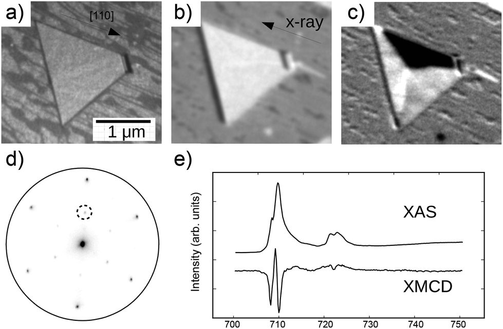 | ||
| Fig. 1 (a) LEEM image of a magnetite island on an FeO wetting layer on Ru(0001). The electron energy is 8 eV. (b) XAS image of the same area, acquired at a photon energy close to the maximum of the L3 Fe absorption edge. (c) X-ray magnetic circular dichroism image of the same area. (d) Low-energy electron diffraction pattern acquired from the island at 30 eV. One of the diffracted beams characteristic of the spinel phase is shown by a circle. (e) Top, the XAS spectrum from the island showing the L3 and the L2 iron edges (averaging spectra with opposite circular polarizations). Bottom, the XMCD spectrum (from the upper black domain in (c)). | ||
From a stack of PEEM images acquired at different photon energies, an XAS spectrum showing the iron L3 and L2 absorption edges can be acquired from the island (see Fig. 1e). It has the typical shape of magnetite,23 with a small shoulder before the main peak at the L3 edge, and a double peak structure at L2. The difference between the XAS spectra acquired with opposite light helicities from a single domain gives the corresponding XMCD spectrum shown at the bottom of Fig. 1e. The XMCD spectrum at both L3 and L2 has a distinctive peak structure (two downward peaks separated by one upward peak in between for L3) as reported previously for magnetite.22–24 The ratio of the peaks indicates a slightly non-stoichiometric character of the Fe![[thin space (1/6-em)]](https://www.rsc.org/images/entities/char_2009.gif) :O ratio, while at the same time ruling out a maghemite composition (which should show a much less pronounced first downward peak23). The spin and the orbital moment of iron in the island can be estimated from the XMCD and XAS spectra through the use of the sum rules25 once the magnetization orientation of the magnetic domains is known as XMCD observations in PEEM are performed in remanence, and only the component of the magnetic moment along the beam is measured. As determined below, the upper domain (shown in black in Fig. 1c) is aligned opposite of the X-ray beam direction. The application of the sum rules (disregarding the dipole operator)25 provides an estimated magnetic spin moment of 3.80μB with a small orbital moment of 0.03μB (Fig. S3†), slightly reduced from the one expected for bulk magnetite as often measured on magnetite surfaces and films depending on the particular state of the surface.26
:O ratio, while at the same time ruling out a maghemite composition (which should show a much less pronounced first downward peak23). The spin and the orbital moment of iron in the island can be estimated from the XMCD and XAS spectra through the use of the sum rules25 once the magnetization orientation of the magnetic domains is known as XMCD observations in PEEM are performed in remanence, and only the component of the magnetic moment along the beam is measured. As determined below, the upper domain (shown in black in Fig. 1c) is aligned opposite of the X-ray beam direction. The application of the sum rules (disregarding the dipole operator)25 provides an estimated magnetic spin moment of 3.80μB with a small orbital moment of 0.03μB (Fig. S3†), slightly reduced from the one expected for bulk magnetite as often measured on magnetite surfaces and films depending on the particular state of the surface.26
In order to obtain the spatially resolved magnetization vector from this and other islands, three consecutive XMCD images are acquired at different azimuthal angles of the sample relative to the X-ray beam. From these, correcting for distortions and transforming from the skew reference axis of the three X-ray incoming directions, a vector map proportional to the local magnetization can be obtained.†27,28. In Fig. 2 the vector dichroic signal (which we will refer to as the vector magnetization map from now on) of the island shown in Fig. 1 as well as neighbor islands is presented, using a color scale for the in-plane azimuthal magnetization angle. For convenience, the different islands will be referred to by their label in this figure throughout the manuscript. The patterns differ strongly from island to island. For example consider islands a and b; despite having a similar shape, orientation, and size, differences can be observed in their patterns. In all cases the magnetization is in-plane.
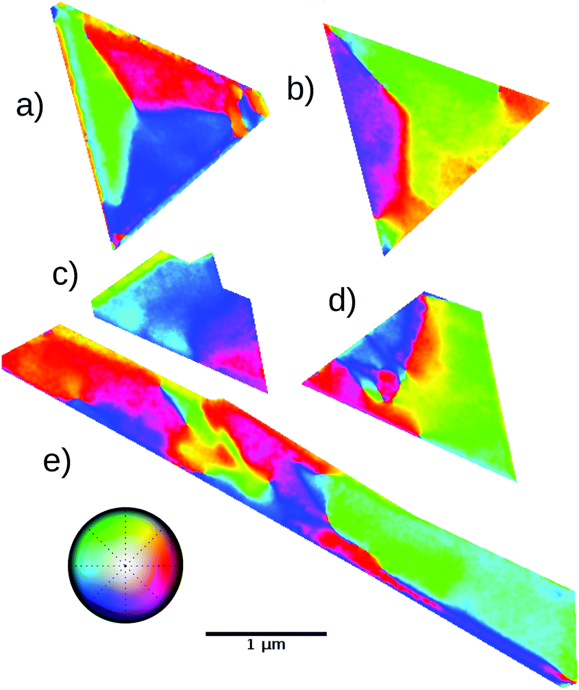 | ||
| Fig. 2 Magnetic domains measured by XMCD-PEEM of a few islands close to that in Fig. 1. For each island, the color scale indicates the azimuthal angle of the magnetization vector. Each island is labeled from (a) to (e). The lateral scale is the same for all islands. | ||
Island a is the only one with a clear shadow in the XAS image (Fig. 1b). It presents a flux closure domain configuration: three magnetic domains of a similar size divide the triangle into three sectors, within which the magnetization is aligned roughly along the side of the nearest edge. The island edges are aligned with the most compact directions of the magnetite unit cell in the (111) plane, namely the in-plane 〈110〉 ones.22 Thus the magnetization is roughly aligned with in-plane 〈110〉 directions. Considering the sequence of magnetic domains, the magnetization curls around in a clockwise sense, minimizing the stray field. The domain walls have a width of 80 ± 10 nm, and are oriented along the bisectrixes of the triangle, i.e. along the in-plane 〈112〉 directions. The domain wall magnetization direction is halfway between the magnetization directions of the adjacent domains, which in turn are at 120° with respect to one another. Islands b, c, d and e are thinner than 15 nm. Island b does not present a fully developed flux closure domain state but has two large domains, again mostly aligned with the triangle top and left edges. In contrast, the third side sector has, instead of a unique domain, a complex multidomain structure with extended domain walls. We lack any detailed height information, as it does not present a shadow in the XAS image (not shown) so it is less than 15 nm. A possible origin of this structure is that the island is not flat, but rather has a wedge shape with the third side being thinner, as found for similar systems.13 The domain wall separating the two large domains starts along the bisectrix of the triangle, but in this case the sense of the wall magnetization changes before reaching the triangle center. Shortly after the sense change, the wall becomes broader and turns down towards the lower bisectrix. Disregarding the small domain at the corner, the chirality of the domains is opposite to the previous island, rotating counterclockwise.
Island c has a more irregular shape. It presents a large domain comprising most of the island, and a smaller one on the lower-right corner, with an ill-defined domain wall between them. Island d is a truncated triangle with two main domains, oriented along the respective island edges (green and blue), and a smaller (red) one on the lower left corner. The wall between the two large domains is extremely wide, being almost another domain by itself (yellow-red area in between).
The last island to be discussed, e, has a very different aspect ratio: it is a stripe 5.5 μm long and 0.5 μm wide. It presents several interlocked domains showing several changes in the chirality of the domain walls between them. Most of the island is covered with domains, reddish or greenish, aligned roughly with the island main axis.
In order to gain further insight into the observed magnetic domain distribution in the islands, micromagnetic simulations have been performed on flat islands with the same shape and size as the experimental ones. The values of the exchange stiffness, saturation magnetization and magnetocrystalline anisotropy were initially set to the values typically used for bulk magnetite:19Aex = 2.64 × 10⁻¹¹ J m−1, Ms = 4.8 × 10⁵ A m−1, and KC1 = −1.25 × 10⁴ J m−3 respectively. The in-plane size of the micromagnetic simulation cell has been assigned to the experimental pixel size of the XAS images (8.4 nm wide), while its height is 11 nm. To check the effects due to the cell size, smaller cells have also been used, both in-plane (down to 4.2 nm) and out-of-plane (down to 2.2 nm), without significant differences. While island a has been simulated with an island thickness corresponding to the experimental one (three cells high), the thinner ones, which experimentally have a height of less than 15 nm, have been simulated with a single cell height of 11 nm. The magnetocrystalline anisotropy axes have been assigned to the room temperature 〈111〉 bulk magnetite ones, together with the known orientation of the islands, which have a (111) orientation and sides along the in-plane 〈110〉 directions.
The experimentally determined magnetization distribution obtained from XMCD-PEEM (Fig. 2) has been used as the initial magnetization configuration. Then the magnetic configuration was relaxed to minimize the energy and then the total torque, using a Bogacki–Shampine solver with the MuMax3 code.18 Thus we expect that the relaxed configurations correspond to local minima, but not necessarily to global minima. The results are shown in Fig. 3. The pattern for island a is very similar to the experimentally observed one: a flux closure domain configuration with a sequence of green/red/blue domains. In each domain the magnetization is aligned along the closer island edge. The domain walls have constant sense up to the vortex-like meeting point.
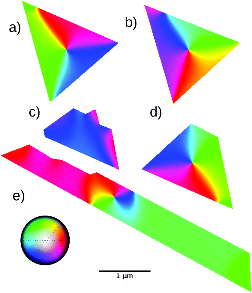 | ||
| Fig. 3 Micromagnetism relaxed configurations, using the experimental configurations as initial ones and employing the known material parameters of bulk magnetite. The micromagnetic simulations were performed on flat islands with the same shape as the experimental ones and with a height of respectively 33 nm (a), and 11 nm (b–e, rest of the islands). | ||
As mentioned before, the experimental width of the domain walls for island a is on average 80 ± 10 nm (both before and after the annealing step to be discussed below). A typical cut across a domain wall is shown in Fig. 4a. The width of the domain walls from the simulations with the bulk magnetite material parameters is very close and slightly wider in average, 100 nm (a profile from the relaxed configuration is shown as a line in the same figure). We consider it instructive to explore the material parameters in order to check their influence on the domain wall width. The results of the simulations, changing the saturation magnetization, the thickness, the magnetocrystalline anisotropy and the exchange stiffness, respectively, are shown in Fig. 4b–e. We note that, except for very low values of the saturation magnetization which give a uniform domain (Fig. 4b), in all other cases the domain structure is very similar: a flux closure domain pattern with domain walls in between. In particular as the saturation magnetization increases, the domain wall width decreases (Fig. 4b). The estimate of the magnetic moment from the XMCD is in good agreement with the bulk value, so there is no reason to suspect an enhanced saturation magnetization as reported29 and disputed30 for ultrathin films. The island thickness influences the domain wall width (Fig. 4c), but in order to decrease the width to the experimental value we would need a height which clearly does not correspond to the one estimated experimentally. The other two remaining parameters are the magnetocrystalline anisotropy and the exchange stiffness: either increasing the magnitude of the magnetocrystalline anisotropy, as shown in Fig. 4d, or decreasing the exchange stiffness (Fig. 4e) would decrease the wall width. We note that the islands are not perfectly stoichiometric, so some differences in the material parameters can be expected. More surprising is that the agreement is quite good without the introduction of either surface or interface anisotropies. This behavior is in contrast to nanometer thick magnetite islands where sharp domain walls have been reported,22 presumably due to interface effects.
 | ||
| Fig. 4 (a) Profile of the XMCD asymmetry across a domain wall (along the blue line shown in the inset), shown with blue dots. The continuous line plot is a profile on the same domain wall after relaxing the experimental configuration in a micromagnetic model with the material parameters of bulk magnetite. Evolution of the domain wall width with (b) saturation magnetization, (c) thickness, (d) magnetocrystalline anisotropy and (e) exchange stiffness (e), respectively, from micromagnetic simulations on island a. The red point corresponds to the experimental configuration. | ||
Most of the other islands relax to some type of flux closure domain pattern, with wider domain walls expected from a reduced thickness. Island b has two wide domains in similar orientation to the experimental ones (green in the upper side, purple in the left one), but the boundary between them is wider than the experimental case. The smaller domains of the right hand side of the triangle disappear in the relaxed configuration. However, island c, the most trapezoidal one, keeps a mostly single domain configuration with some smaller domains in the right edges. This configuration seems to be locked in place both experimentally and in the micromagnetic simulation by the small lateral size together with the reduced thickness.
Relaxing island d results in the removal of the complicated combination of domains experimentally observed, and the appearance of a flux closure vortex-like domain configuration. Finally the stripe-shaped island relaxes to a multidomain configuration, with the left most side of the island oriented in one sense (red-purple) and the right-most with the opposite sense (green). The boundary between them, a complex section with very sharp domain walls in the experiment, relaxes to extended domain walls in a vortex configuration. We note however that the lowest energy configuration in this case is a single domain, as found by starting from a random magnetization.
To experimentally study the stability of the magnetic domains, the sample was demagnetized by annealing above the Curie temperature, for 15 minutes at 1070 K. In order to prevent a reduction of the magnetite islands, expected from heating in vacuum, the annealing of the islands was performed in 10−5 mbar of molecular oxygen, and cooled down until the temperature decreased below 773 K in the same background gas. In Fig. 5, island a is shown again after the annealing step. This island has only minor changes in the shape, as seen in the LEEM image (Fig. 5a). It shows now truncated corners. The XAS image shows the shadow on the left hand side, and the domains are observed again in the XMCD-PEEM image, with the same apparent distribution as before. The LEED pattern does not show any changes and is still characteristic of an spinel phase. The XAS spectrum is indistinguishable from the previous one, and thus corresponds to a mixed Fe2+ and Fe3+ oxide phase. The XMCD-PEEM shows a somewhat different ratio of the downward peaks, still indicative of slightly non-stoichiometric magnetite.24
 | ||
| Fig. 5 (a) LEEM image of the island shown in Fig. 1 after annealing (acquired at 8 eV). (b) XAS image of the same area, acquired at a photon energy close to the maximum of the L3 Fe adsorption edge. (c) X-ray magnetic circular dichroism image of the same area. (d) Low-energy electron diffraction pattern acquired from the island at 30 eV. (e) Top, XAS spectrum from the island showing the L3 and the L2 iron edges (averaging spectra with opposite circular polarizations). Bottom, XMCD spectrum (from the upper black domain in (c)). | ||
Through this annealing, however, the size and height of the rest of the islands change considerably, as detected by comparing Fig. 6 and 2 (or Fig. S4†). The changes are more evident the smaller the island was initially. Island a, initially 33 nm thick, is now 44 nm thick, and has shrinked by 9% in area. Islands b and c have now a detectable shadow (not shown), corresponding to a height of 15 nm, while their areas have decreased by 12–15%. Islands d and e have lost more area, up to 40% for the smallest one, while both are still thin enough that no shadow is seen. The evolution of the different islands can be explained by a combination of the tendency towards three-dimensional growth and a coarsening effect: upon annealing it is expected on one hand that the material will tend to flow towards the top of the islands and, on the other hand, that the material leaves the smaller islands and flows to the larger ones. The lateral size, which is the one directly observable, is expected to change more in the thinner and smaller islands, as observed.
 | ||
| Fig. 6 Magnetic domains experimentally observed on the same islands shown in Fig. 2 after annealing the substrate for 15 minutes to 1073 K. Some changes in the islands shape are apparent, specially in the smaller ones and in the striped island which is much narrower after the annealing. | ||
The island that shows the least changes in the magnetic domain distribution is island a: the same three (green/red/blue) domains aligned along the sides of the island are observed after annealing. Even the domain walls have a similar character, although their orientation has changed slightly. However, the rest of the islands have changed significantly. Island b now only presents two domains with a curved domain wall between them. The two smaller islands (c and d) present large domains with wide, meandering domain walls as before, but with patterns unrelated to the original ones. Finally, the striped island after annealing is narrower and is now single domain, with the magnetization along the principal axis of the island, as expected from shape anisotropy. We then again introduced the experimental magnetization patterns as the initial configuration of micromagnetic simulations employing the new shapes and heights. The results are shown in Fig. 7. Island a, as was the case before annealing, shows in the simulation the same pattern as the experiment with a closure domain configuration. Island e, which is now single domain in the experiment, is also a single domain in the simulation. The two other larger compact islands, b and c, are now very similar to the calculated configurations. They each show two domains that split each island in two. However, while in the simulations the domain wall between them is straight, in the experiment it is curved, specially for island b. Finally, island d reverts to a single domain configuration in the simulation while there is a small domain on one side in the experiment.
 | ||
| Fig. 7 Micromagnetism relaxed configurations, using the experimental configurations observed after annealing. As before, the micromagnetic simulations were performed on flat islands with the same shape and height as the experimental ones. | ||
Thus the micromagnetic simulations with bulk magnetic parameters compare well with the XMCD-PEEM magnetic domain observations, accurately explaining the behavior of the magnetite islands, especially if the islands are demagnetized after growth and left to relax magnetically. The magnetization is mostly parallel to the sides of the islands. This is more clear in the tallest island a, which has a flux closure domain configuration to minimize the stray field. This island behaves like bulk magnetite and has well defined magnetic domains separated by narrow domain walls. The magnetization of each domain is oriented along the island edge closer to it, both in the experimental case and in the relaxed micromagnetic configuration. This implies that the shape anisotropy overcomes the magnetocrystalline anisotropy, which would tend to align the magnetization along the bisectrix of the triangle (the projection of the bulk 〈111〉 axes on the (111) plane i.e., 〈112〉 directions). Another island where the experimental magnetization patterns nicely match the predictions of the simulations is the stripe-shaped island: the change from a multidomain to a single domain in such an island can be understood by the modification of the island dimensions and the removal of kinetic limitations by annealing. In this case, the shape anisotropy clearly dictates the final distribution of the magnetization.
The rest of the islands are much better reproduced in the micromagnetic simulations after the demagnetization step. This implies that during the growth and the cooling down, their magnetization patterns got “stuck” in configurations that are not the minimum energy ones. Only after the annealing–demagnetization step do they fall into a magnetically relaxed configuration, closely resembling the calculated ones.
In general the observation that these islands behave mostly as expected from the known properties of bulk magnetite strongly supports that the islands do not have antiphase boundaries or other defects that would pin the domain walls.
Conclusions
We have determined the magnetization of in situ grown magnetite islands by means of XMCD-PEEM with a resolution of 20 nm. The islands arise from single nuclei and thus are expected to be free of growth defects such as anti-phase domain boundaries. The experimental magnetization distribution has been compared with the micromagnetic simulations of objects with the same shape and initial magnetization. It has been found that for several cases their behavior can be completely understood taking into account only the known magnetic properties of bulk defect-free magnetite and its shape, specially for the thicker island. Together with the weak magnetocrystalline anisotropy, these result in shape-anisotropy-defined spin configurations, potentially allowing the design of nanostructures with desired magnetization patterns. Magnetite magnetic bulk properties have been achieved in a nanostructured environment.Conflicts of interest
There are no conflicts to declare.Acknowledgements
This work is supported by the Spanish Ministerio de Economía y Competitividad through Projects no. MAT2013-48009-C4-1-P, MAT2014-52477-C5-2-P, MAT2015-64110-C2-1-P, and MAT2015-64110-C2-2-P and by the European Comission through Project H2020 no. 720853 (Amphibian). These experiments were performed at the CIRCE beamline of the ALBA Synchrotron Light Facility. I. P. acknowledges the EU via the innovation program under grant agreement no. 696656 (GrapheneCore1-Graphene-based disruptive technologies).References
- R. M. Cornell and U. Schwertmann, The Iron Oxides, John Wiley & Sons Ltd, 1997, p. 604 Search PubMed.
- P. Weiss and R. Forrer, Ann. Phys., 1929, 12, 279 CAS.
- D. T. Margulies, F. T. Parker, F. E. Spada, R. S. Goldman, J. Li, R. Sinclair and A. E. Berkowitz, Phys. Rev. B: Condens. Matter Mater. Phys., 1996, 53, 9175–9187 CrossRef CAS.
- F. C. Voogt, T. T. M. Palstra, L. Niesen, O. C. Rogojanu, M. A. James and T. Hibma, Phys. Rev. B: Condens. Matter Mater. Phys., 1998, 57, R8107 CrossRef CAS.
- E. Arenholz, G. van der Laan, R. V. Chopdekar and Y. Suzuki, Phys. Rev. B: Condens. Matter Mater. Phys., 2006, 74, 094407 CrossRef.
- M. Monti, M. Sanz, M. Oujja, E. Rebollar, M. Castillejo, F. J. Pedrosa, A. Bollero, J. Camarero, J. L. F. Cuñado, N. M. Nemes, F. J. Mompean, M. Garcia-Hernández, S. Nie, K. F. McCarty, A. T. N'Diaye, G. Chen, A. K. Schmid, J. F. Marco and J. de la Figuera, J. Appl. Phys., 2013, 114, 223902 CrossRef.
- P. Prieto, J. de la Figuera, L. Martín-García, J. E. Prieto and J. F. Marco, J. Mater. Chem. C, 2016, 4, 7632–7639 RSC.
- D. T. Margulies, F. T. Parker, M. L. Rudee, F. E. Spada, J. N. Chapman, P. R. Aitchison and A. E. Berkowitz, Phys. Rev. Lett., 1997, 79, 5162 CrossRef CAS.
- W. Eerenstein, T. T. M. Palstra, T. Hibma and S. Celotto, Phys. Rev. B: Condens. Matter Mater. Phys., 2003, 68, 014428 CrossRef.
- W. Eerenstein, Ph.D. thesis, Rijskuniversisteit, Groningen, 2003.
- T. Kasama, R. Dunin-Borkowski and W. Eerenstein, Phys. Rev. B: Condens. Matter Mater. Phys., 2006, 73, 104432 CrossRef.
- J.-B. Moussy, J. Phys. D: Appl. Phys., 2013, 46, 143001 CrossRef.
- L. Martín-García, A. Quesada, C. Munuera, J. F. Fernández, M. García-Hernández, M. Foerster, L. Aballe and J. de la Figuera, Adv. Mater., 2015, 27, 5955–5960 CrossRef PubMed.
- L. Aballe, M. Foerster, E. Pellegrin, J. Nicolas and S. Ferrer, J. Synchrotron Radiat., 2015, 22, 745–752 CrossRef CAS PubMed.
- E. Bauer, Surface Microscopy with Low Energy Electrons, Springer, Berlin Heidelberg, 2014 Search PubMed.
- C. M. Schneider and G. Schönhense, Rep. Prog. Phys., 2002, 65, 1785–1839 CrossRef.
- I. Palacio, M. Monti, J. F. Marco, K. F. McCarty and J. d. l. Figuera, J. Phys.: Condens. Matter, 2013, 25, 484001 CrossRef CAS PubMed.
- A. Vansteenkiste, J. Leliaert, M. Dvornik, M. Helsen, F. Garcia-Sanchez and B. V. Waeyenberge, AIP Adv., 2014, 4, 107133 CrossRef.
- W. Williams and T. M. Wright, J. Geophys. Res., 1998, 103, 30537–30550 CrossRef CAS.
- W. Weiss and W. Ranke, Prog. Surf. Sci., 2002, 70, 1–151 CrossRef CAS.
- G. S. Parkinson, Surf. Sci. Rep., 2016, 71, 272–365 CrossRef CAS.
- M. Monti, B. Santos, A. Mascaraque, O. Rodríguez de la Fuente, M. A. Niño, T. O. Mentes, A. Locatelli, K. F. McCarty, J. F. Marco and J. de la Figuera, Phys. Rev. B: Condens. Matter Mater. Phys., 2012, 85, 020404 CrossRef.
- E. Pellegrin, M. Hagelstein, S. Doyle, H. Moser, J. Fuchs, D. Vollath, S. Schuppler, M. James, S. Saxena, L. Niesen, O. Rogojanu, G. Sawatzky, C. Ferrero, M. Borowski, O. Tjernberg and N. Brookes, Phys. Status Solidi B, 1999, 215, 797–801 CrossRef CAS.
- P. Morrall, F. Schedin, G. S. Case, M. F. Thomas, E. Dudzik, G. van der Laan and G. Thornton, Phys. Rev. B: Condens. Matter Mater. Phys., 2003, 67, 214408 CrossRef.
- C. T. Chen, Y. U. Idzerda, H.-J. Lin, N. V. Smith, G. Meigs, E. Chaban, G. H. Ho, E. Pellegrin and F. Sette, Phys. Rev. Lett., 1995, 75, 152–155 CrossRef CAS PubMed.
- L. Martín-García, R. Gargallo-Caballero, M. Monti, M. Foerster, J. F. Marco, L. Aballe and J. de la Figuera, Phys. Rev. B: Condens. Matter Mater. Phys., 2015, 91, 020408 CrossRef.
- L. Le Guyader, A. Kleibert, A. Fraile Rodríguez, S. El Moussaoui, A. Balan, M. Buzzi, J. Raabe and F. Nolting, J. Electron Spectrosc. Relat. Phenom., 2012, 185, 371–380 CrossRef CAS.
- X. Moya, L. E. Hueso, F. Maccherozzi, A. I. Tovstolytkin, D. I. Podyalovskii, C. Ducati, L. C. Phillips, M. Ghidini, O. Hovorka, A. Berger, M. E. Vickers, E. Defay, S. S. Dhesi and N. D. Mathur, Nat. Mater., 2013, 12, 52–58 CrossRef CAS PubMed.
- S. K. Arora, H. C. Wu, R. J. Choudhary, I. V. Shvets, O. N. Mryasov, H. Yao and W. Y. Ching, Phys. Rev. B: Condens. Matter Mater. Phys., 2008, 77, 134443 CrossRef.
- J. Orna, P. A. Algarabel, L. Morellon, J. A. Pardo, J. M. de Teresa, R. Lopez Anton, F. Bartolome, L. M. Garcia, J. Bartolome, J. C. Cezar and A. Wildes, Phys. Rev. B: Condens. Matter Mater. Phys., 2010, 81, 144420 CrossRef.
Footnote |
| † Electronic supplementary information (ESI) available: Additional methods information. See DOI: 10.1039/C7NR07143D |
| This journal is © The Royal Society of Chemistry 2018 |