
Homo-endotaxial one-dimensional Si nanostructures†‡
Jiaming
Song
 a,
Bethany M.
Hudak
a,
Hunter
Sims
ab,
Yogesh
Sharma
a,
T. Zac
Ward
a,
Sokrates T.
Pantelides
ab,
Andrew R.
Lupini
a and
Paul C.
Snijders
*ac
a,
Bethany M.
Hudak
a,
Hunter
Sims
ab,
Yogesh
Sharma
a,
T. Zac
Ward
a,
Sokrates T.
Pantelides
ab,
Andrew R.
Lupini
a and
Paul C.
Snijders
*ac
aMaterials Science and Technology Division, Oak Ridge National Laboratory, Oak Ridge, Tennessee 37831, USA. E-mail: snijderspc@ornl.gov
bDepartment of Physics and Astronomy and Department of Electrical Engineering and Computer Science, Vanderbilt University, Nashville, Tennessee 37235, USA
cDepartment of Physics and Astronomy, The University of Tennessee, Knoxville, Tennessee 37996, USA
First published on 29th November 2017
Abstract
One-dimensional (1D) nanostructures are highly sought after, both for their novel electronic properties as well as for their improved functionality. However, due to their nanoscale dimensions, these properties are significantly affected by the environment in which they are embedded. In this paper, we report on the creation of 1D homo-endotaxial Si nanostructures, i.e. 1D Si nanostructures with a lattice structure that is uniquely different from the Si diamond lattice in which they are embedded. We use scanning tunneling microscopy and spectroscopy, scanning transmission electron microscopy, density functional theory, and conductive atomic force microscopy to elucidate their formation and properties. Depending on kinetic constraints during growth, they can be prepared as endotaxial 1D Si nanostructures completely embedded in crystalline Si, or underneath a stripe of amorphous Si containing a large concentration of Bi atoms. These homo-endotaxial 1D Si nanostructures have the potential to be useful components in nanoelectronic devices based on the technologically mature Si platform.
Introduction
The promise of novel physical properties in low-dimensional and nanoscale electronic systems, as well as the increasingly demanding requirements instigated by the continuing miniaturization of electronic devices, have resulted in a concentrated effort in the synthesis of one-dimensional (1D) nanostructures.1–8 This effort has become even more urgent within the context of quantum computation, in particular for the approach proposed by Kane9,10 where closely spaced single donor atoms have to be electronically addressed with well-defined electric fields within a Si matrix. It is possible to fabricate nanostructures at the atomic scale using top-down approaches based on scanning tunneling microscopy (STM)11–13 or scanning transmission electron microscopy (STEM).14 However, such processes are necessarily serial in nature, limiting the flexibility in design and volume of these structures. On the other hand, epitaxial nanowires with large aspect ratios and atomically abrupt interfaces can be synthesized in parallel using self-organization processes on surfaces,1,15 using vapor–liquid–solid growth processes,16 or in solution.17 Regardless of synthesis pathways, the relatively large number of exposed surface atoms leaves 1D nanostructures very sensitive to adsorbing species from the ambient environment. In particular, nanostructures that are fabricated either from Si or on Si surfaces are highly susceptible to adsorbed species. As a result, a protective capping layer, e.g. via molecular surface passivation,18 is necessary to protect the nanostructures, preferably without the introduction of new elements to the system.In this paper we report direct evidence for the synthesis of 1D homo-endotaxial Si nanowires grown on Si(100), i.e. crystallographically distinct 1D Si nanostructures that are endotaxially embedded in a Si film grown on a commercial Si(100) wafer. These homo-endotaxial nanowires therefore do not have surface atoms that are exposed to the ambient. Our approach builds on the stability of the reconstructed Si “Haiku” core structure19 present below Bi nanolines grown on the Si(100) surface in conjunction with the poor solubility of Bi in the Si capping layer.23,24 Furthermore, by limiting the Bi diffusion in Si we also synthesize embedded 1D heterostructures consisting of a 1D reconstructed Si core below a stripe of amorphous Si (a-Si) containing a large concentration of Bi atoms.
When viewed along the [110] direction, i.e. along the axis of the nanoline, the Haiku core structure underneath the surface Bi nanolines consists of a semicircle of three 5-membered and two 7-membered rings, filled by one 6-membered ring.19 The self-organization of Bi nanolines on Si(100) was reported in a pioneering paper by Miki et al.,1 and the driving force for their formation and their subsurface Si “Haiku” core structure was elucidated by Owen et al.19 While encapsulation of these Bi nanolines inside a Si crystal has been pursued before,20–22 their survival upon capping and the resulting nanoline structure have remained ambiguous. Saito et al. used the X-ray standing wave (XSW) technique to probe possible structures of Bi nanolines on Si(100) capped at room temperature by a-Si.20 Based on a fit of XSW data to a model that assumed that the Bi atoms are still ordered after capping, they infer the presence of a continuous nanoline structure including Bi dimers after capping. However, no direct experimental observations of the lattice were available to corroborate this analysis. Miki et al. reported that Bi nanolines can be successfully buried inside an epitaxial crystalline Si (c-Si) film grown at 400 °C when using a Bi surfactant layer.21 However, their secondary ion mass spectroscopy data only reveal a (rather thick) buried Bi layer, and their electron microscopy data are of insufficient clarity to provide direct evidence for the presence of buried Haiku-cores or Bi nanolines. Later, Sakata et al. used X-ray diffraction on Bi nanolines also capped by c-Si using a Bi surfactant layer,22 and aided by DFT calculations they infer that the Si Haiku-core reconstruction does not survive, but that the Bi atoms do remain 1D ordered.22 Clearly, these conflicting results on the feasibility of creating these embedded nanostructures highlight the need for direct experimental evidence to ascertain whether embedded 1D Si and/or Bi nanostructures can be synthesized.
Using detailed atomically resolved STM and Z-contrast STEM imaging of the Bi atoms in the Si, we reveal that the Bi nanolines do not survive upon Si overgrowth, even when a low-temperature solid phase epitaxial overgrowth approach is used. Instead, cross-sectional STEM imaging clearly shows that the Bi atoms diffuse away from their location on top of the Si Haiku core of the original Bi nanolines,19 enabling the exploitation of kinetic constraints during Si overgrowth to control the extent of the Bi distribution in the capping layer. Moreover, our data show that the unique lattice of the Si Haiku core, containing of 5- and 7-membered rings, expands into the capping layer depending on its growth temperature, creating larger homo-endotaxial nanostructures. Finally, our DFT calculations indicate that the unique Si lattice of these nanostructures features an electronic gap that is ∼300 meV smaller than that of bulk Si, which is consistent with the observation of highly conducting stripes in our conductive atomic force microscopy data. The formation of these small bandgap 1D Si nanostructures that are protected from the environment by their embedding inside a Si lattice demonstrates that kinetic growth control allows for the creation of uniquely novel nanostructures.
Results and discussion
We first present a characterization of the Bi nanoline template surface in order to establish that our starting point indeed corresponds to the Bi nanolines that have been reported before1,19,25 and to provide a benchmark against which to compare the structures found after Si overgrowth. The Si(100) substrate with Bi nanolines on its surface, visible as relatively bright straight lines in STM imaging of the terraces of the Si(100) surface, is shown in Fig. 1a. Following the Si(100) surface symmetry, the Bi nanolines form two orthogonal domains on different Si terraces that are separated by a single step edge. On our samples, the spacing between these nanolines can vary from several tens to just a few nanometers. In the LEED pattern shown in the inset, the presence of the Bi nanolines is apparent in the streaks connecting the (2 × 1) spots from the substrate. Fig. 1b shows a higher resolution STM image of the Bi nanoline structure on the (2 × 1) reconstructed Si(100) surface. The Bi nanolines are orthogonal to the Si dimer rows which rotate 90° on adjacent terraces with a height difference of one monolayer (ML). The separation of the two linear features visible within the Bi nanolines is ∼6.38 Å (Fig. 1d), consistent with earlier reports,19,25,26 and the measured distance between the two nearest Si dimers is 18.2 Å, in excellent agreement with the Haiku model for the Bi nanolines,19 as shown in the inset of Fig. 1d. The lines of Bi atoms on the surface are semiconducting,27 with a larger bandgap than that of the surrounding bare Si(100)-(2 × 1) surface (Fig. 1e), and have a brighter contrast than the Si(100) surface in the dI/dV map recorded at larger negative biases27 (Fig. 1c). | ||
| Fig. 1 (a) Large-scale STM topography image of Bi nanolines on Si(100) substrate. STM scanning parameters: −1.85 V, 190 pA. The inset is a LEED pattern from the same surface, recorded at 100 eV. (b) High-resolution STM topography image and (c) simultaneously recorded differential conductance map of Bi nanolines on Si(100) (2 × 1) reconstructed surface (tunneling parameters −2.5 V, 400 pA). (d) Line profile recorded as indicated in (b). The inset at the bottom shows the Haiku core structure. (e) I(V) curves taken from a Bi nanoline and the vicinal Si(100) surface (setpoint −1.5 V, 500 pA). Red and blue down-pointing arrows indicate bandgap edges for Si and Bi, respectively. | ||
Next, we deposit a Si layer on this Bi nanoline surface to encapsulate the nanoline structure. We explored different capping layer growth parameters and subsequently analyzed the resulting structures with high-resolution Z-contrast STEM. Approaches proposed in previous reports20–22,28 suggest that Bi nanolines can be buried intact in epitaxially grown c-Si when, to prevent the Bi atoms of the nanoline from diffusing away, additional Bi is deposited on the surface as a surfactant, or if the overgrowth is performed at relatively low temperatures. Our observations following these synthesis approaches reported in the literature are presented in ESI note 1 and Fig. S1a–c.‡
Growing the capping layer at room temperature (Fig. 2a)20 predictably results in an amorphous film. However, inspection of the atomic structure at the interface between the crystalline substrate and this amorphous capping layer reveals local changes from the Si diamond lattice that resemble the Haiku core of the Bi nanolines, as further discussed below, without the double rows of Bi atoms that are visible in STM images (Fig. 1a and b). Instead, the a-Si capping layer contains randomly distributed Bi atoms, visible as brighter features in the Z-contrast STEM images, with a locally larger concentration near the reconstructed Si cores. In Fig. 2 (also Fig. S1 in the ESI‡), based on the amount of Bi in the as-grown sample, the proximity of the bright regions to the core structures, and the location of the bright regions at the interface where the Bi should be located, we can conclude that these bright regions are Bi atoms that have diffused into the a-Si capping layer. Because of electron beam channeling in the STEM, the substitutionally doped Bi atoms contained in the Si columns appear as sharp, white dots (Fig. 2b) that are brighter than the single Bi atoms in the amorphous matrix, such as those in the capping layer in Fig. 2a. These data demonstrate that the Bi atoms have a finite mobility in the Si capping layer, even during capping layer growth at temperatures as low as room temperature, and that the Si core structure of the nanolines can survive if the capping layer growth temperature is sufficiently low. As this results in a poorly defined amorphous overlayer in contact with the buried Si nanostructure, we have utilized a two-step solid phase epitaxial (SPE) capping layer growth process in order to cap the Si core structure with a crystalline overlayer. In particular, we deposited a 2.3 nm a-Si overlayer at room temperature, and subsequently flash-annealed the sample at 430 °C for 5 s until it had crystallized, as evidenced in situ by the appearance of a (2 × 1) reconstructed (001) surface29 (Fig. 3a). A thicker amorphous capping layer was deposited next at temperatures below −128 °C to protect the thin crystalline structure during STEM specimen preparation. STEM imaging reveals similar Si core structures, now endotaxially embedded in a thin crystallized capping layer, see Fig. 2b. Some Bi atoms are visible; a few in the crystalline capping layer, and the remainder in lower regions of the amorphous overlayer. These results for the first time directly demonstrate that it is possible to create homo-endotaxial 1D Si nanostructures buried below the sample surface. In Fig. 2a (also Fig. S1‡), the bright circular blobs of about 4 nm diameter in the substrate region are likely due to material redeposition during mechanical sample preparation. It is likely that they are amorphous carbon or silicon.
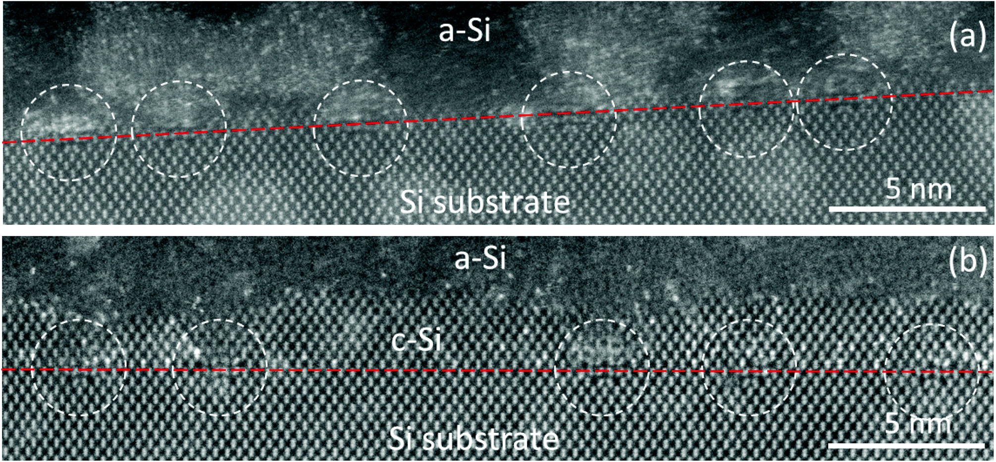 | ||
| Fig. 2 Cross-sectional STEM images for Si(100) substrates with Bi-induced nanolines viewed down the [110] axis after (a) capping with Si at room temperature and (b) growing a ∼2.3 nm thick c-Si capping layer using SPE, followed by capping with a-Si at low temperature. The red dashed lines indicate the position of the surface of the original Si(100) substrate before capping as inferred from the reconstructed Si cores. White dashed circles mark reconstructed core structures, which have a similar separation as the Bi nanolines observed in STM. | ||
 | ||
| Fig. 3 (a) STM topography image of 2.3 nm thick c-Si capping layer grown by SPE on Si(100) surface with Bi nanolines. Feedback parameters: −1.8 V, 0.2 nA. (b) High-resolution cross-sectional STEM image of a representative core structure viewed down the [110] zone axis obtained by capping a Si(100) surface with Bi nanolines by a-Si at room temperature. The yellow rectangle marks a unit cell in the (110) plane. For clarity, the inset shows the same area as the main graph without markings. (c) A typical Si nanostructure core viewed down the [110] zone axis grown by the two-step SPE method. The inset also shows the same area as the main graph without markings. The red dashed line indicates the surface of the original Si(100) substrate before capping. | ||
A detailed analysis of high-resolution cross-sectional STEM data in Fig. 3b of the embedded Si nanostructures, consistently shows that this Haiku core structure is modified by the subsequent capping layer growth, see also Fig. 2a and b, and Fig. S1c:‡ two new 7-membered rings are formed above the original surface, creating a modified Haiku core consisting of a larger semicircle of odd-membered rings that is filled by four 6-membered rings. We infer that the Bi atoms that diffuse away during capping layer growth leave behind sites where arriving Si atoms bond epitaxially, allowing for the c-Si growth of a thin layer (∼1 unit cell) of Si even when the capping layer is grown at temperatures that create an otherwise a-Si film,30 see Fig. 2a and Fig. S1c.‡
This scenario is corroborated by DFT calculations of the total energies of the normal and modified Bi-terminated Haiku structures, as well as the Bi-terminated flat Si(100) surface19 as discussed in ESI note 3.‡ These calculations confirm that the original Bi-terminated Haiku core represents the lowest energy state, and therefore that this subsurface structure indeed forms the starting point of the overgrowth, as experimentally ascertained above. The expanded Haiku cores observed in our STEM experiments thus form during capping layer growth. Indeed, when we place a single layer of Si atoms above the normal Bi-terminated Haiku structure and allow the atomic positions to relax, the structure of the Bi lines severely distorts, see Fig. S5.‡ We attribute this tendency of the overgrown Si to displace the Bi nanolines to the difference in binding energies of Si and Bi ad-atoms, as the former are preferred by 1.6 eV per dimer. We conclude that the destruction of the Bi nanolines is partially caused by preferential bonding between the overgrown Si and the existing Si surface. This is a fundamental obstacle to preserving nanostructures with ordered Bi atoms within a Si environment and is not dependent on growth parameters.
The Si cores of the nanostructures embedded in an epitaxial c-Si capping layer (grown using the two-step solid phase epitaxial process, including a larger thermal budget, see also Fig. 2b) are even more expanded, creating embedded 1D Si nanostructures with a larger cross section, see Fig. 3c. As expected from the similarity in growth procedures for the a-Si and c-Si capped nanolines (both are initially covered by an amorphous layer), the initial structure of the c-Si capped nanostructures is similar to that of the a-Si capped structure (compare the blue structure in Fig. 3c with the structure in Fig. 3b). However, the SPE recrystallization of the initially amorphous overlayer breaks the middle 6-membered ring allowing for another layer of 5- and 7-membered rings before reverting to the standard Si lattice of 6-membered rings, see Fig. 3c. While there is some variation in the configuration of 5-, 6-, and 7-membered rings in these embedded endotaxial Si nanostructures that also depends on the degree of crystalline order in the SPE overlayer (see Fig. S3‡), the majority of the nanostructures buried in a crystalline epitaxial Si capping layer features a lattice structure as depicted in Fig. 3c. The occasional continuing growth of odd-membered rings during the post-annealing treatment, and the observed small variation in their topology are consistent with a kinetic stability of the endotaxial structures, i.e. with a significant energy barrier impeding reversion to the Si diamond lattice. This suggests these structures may be robust enough to withstand limited further thermal treatments associated with the growth of contacts or heterostructures. It also implies that further control of the Si core structure would require an even stronger constraining of the crystallization kinetics of the capping layer, which is unlikely to be achieved.
Having elucidated the formation and structure of these endotaxial Si nanowires, their electronic properties are most relevant for potential applications. However, it is experimentally challenging to study the electronic properties of embedded nanostructures that reside several nm below a surface, in particular if they are made of the same element as the host material. We have used C-AFM in order to ascertain whether electronic signatures of the subsurface nanostructures could be detected in a sample that was synthesized with a room temperature a-Si capping layer (see also Fig. 2a). In Fig. 4a we present a current map of a sample with embedded endotaxial 1D Si nanostructures, see also Fig. 2a and 3b. The current map image with buried endotaxial Si nanowires displays sharp linear bright features in two orthogonal domains (as also shown in Fig. S6b‡) that are absent in the topographic image (see Fig. S6a‡) and bear a strong resemblance to the Bi nanoline topography visible in STM images (see Fig. S6c‡). This suggests that the buried nanostructures exhibit a higher conductivity than the surrounding bulk and act as subsurface endotaxial (semiconducting) nanowires.
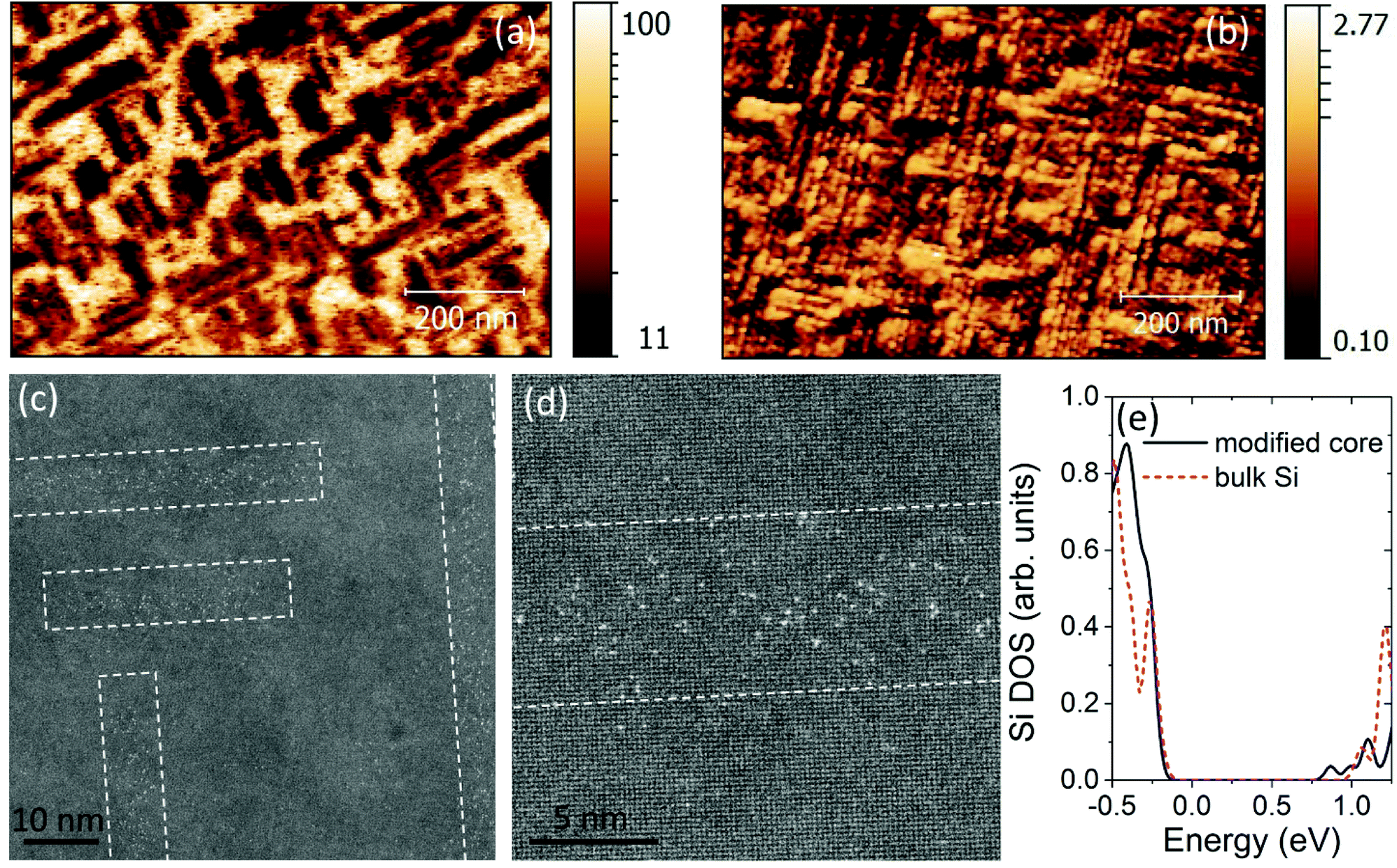 | ||
| Fig. 4 C-AFM current maps obtained on samples with a 6.8 nm a-Si capping layer (a) (DC bias +1.2 V) and a 2.3 nm c-Si capping layer (b) (DC bias +1.5 V) deposited on Si(100) surfaces with Bi nanolines. The different current scales of the maps are likely due to a difference in resistance of the capping layer that is in series with the spatially varying local resistance. The current scale units for both maps are nA. (c) Plan view STEM image viewed down the [100] zone axis of a sample with the same structure as in (a). The white dashed rectangles mark the remnants of the Bi nanolines that were on the substrate before capping. (d) Higher resolution image cropped from the top left stripe area in (c). (e) DFT calculated density of states (DOS) of the Si atoms in the modified Haiku core and bulk Si. Note that the DOS is normalized to the total integrated DOS in a range of −14 to 5.2 eV. | ||
We note, however, that in this sample the Bi atoms that originated from the Bi nanolines are distributed in a small region of the amorphous capping layer near the endotaxial Si wires due to the short diffusion length during capping layer growth at room temperature, see Fig. 2a. This can be more clearly observed in the STEM image in Fig. 4c and d recorded from a similar room-temperature capped nanoline sample. We observe stripes with a width of less than 5 nm and consisting of randomly distributed bright Bi atoms, as indicated by the dashed white boxes in Fig. 4c and better resolved in Fig. 4d. The cross-section view of samples grown under the same conditions (Fig. 2a) indicates that the Bi atoms are located in the a-Si capping layer. Assuming isotropic diffusion of Bi in the a-Si capping layer, this suggests that the diffusion length of the Bi atoms during the growth of the capping layer at room temperature is only ∼2.5 nm. Since Bi atoms are n-type dopants when substitutionally incorporated with a four-fold coordination in the Si lattice, their proximity to the endotaxial Si wires could also potentially explain the increase in conductivity observed in Fig. 4a. Therefore, to find whether the observed increased conductivity originates in the endotaxial Si nanowires or in the stripes of a-Si with a high concentration of Bi atoms, we recorded a C-AFM current map on a sample with endotaxial Si nanostructures under a crystalline capping layer, see Fig. 2b. In these samples, the Bi has mostly desorbed during capping layer growth,1 and the remaining Bi atoms are uniformly distributed, i.e. there are no stripes with a high concentration of Bi atoms as in the a-Si capped samples. Nonetheless, C-AFM maps recorded on such samples, Fig. 4b, also prominently feature lines with a locally higher conductivity. These results show that the locally increased conductivity, detectible even through the (series) resistance of the Si capping layer, is due to the buried endotaxial Si nanostructures having a significantly higher conductivity than the Si matrix.
Our hybrid functional DFT calculations are consistent with this inference. As shown in Fig. 4e, Si atoms within the modified Haiku core contribute gap states that range from approximately 100–300 meV below the bulk Si conduction band edge, depending on the environment surrounding the defect core. Note that while experimentally controlling the structural configuration of the embedded nanowires would require highly constrained crystallization kinetics, the presence of odd-membered rings in all cores likely results in similar electronic properties. The significant reduction of the Si gap for these homo-endotaxial nanostructures essentially creates an endotaxial semiconducting nanowire inside the Si host, and will result in a larger conductivity of the buried nanostructures that is consistent with our C-AFM observations. Our results demonstrate that it is possible to fabricate subsurface 1D heterostructures of narrow-gap endotaxial semiconducting lines, possibly allowing for tailored conduction pathways inside Si.
Conclusion
In conclusion, we have developed a synthesis approach for endotaxially embedded 1D Si nanostructures by utilizing self-assembled Bi nanolines on the Si(100) surface, and validate their presence by directly imaging them using STEM. Specifically, upon capping these homo-endotaxial nanostructures with a-Si, the rows of Bi atoms that were present in the Bi nanoline template do not survive, leaving only the endotaxial 1D Si nanostructures. Moreover, using SPE we can embed these 1D Si nanostructures even in a crystalline Si lattice. Their formation suggests a reasonable kinetic stability, offering opportunities to further incorporate them into more complicated structures requiring additional growth. Our spatially resolved C-AFM measurements show that these homo-endotaxial nanostructures conduct better than the surrounding material, which hybrid functional calculations suggest can be attributed to their significantly narrower band gap as compared to the Si host. Although the spacing between Bi nanolines on Si(100) is aperiodic, their orientation is controllable by creating unidirectional domains on Si(100).26,36 According to the higher conductivity of these 1D endotaxial Si nanowires and the feasibility of controllable orientation, the overall anisotropy of the electronic properties of the sample can potentially be manipulated using single domain surfaces. Moreover, the small dimensions of these nanostructures, their protected subsurface architecture, and their electronic properties can conceivably form the basis for the development of future atomic-scale nanoelectronic components, such as those necessary in quantum bits.Methods
Sample preparation
Si(100) substrates were degassed at 600 °C for around 15 hours in an ultrahigh vacuum system with a base pressure of 5 × 10⁻¹¹ Torr, and then repeatedly flashed at 1150 °C while keeping the pressure lower than 2 × 10⁻⁹ Torr, followed by a slow cool-down from 800 °C to room temperature. The quality of the (2 × 1) reconstructed Si(100) surface was checked by STM and low energy electron diffraction (LEED). Bi with a purity of 99.9999% was evaporated from a thermal evaporator at 486 °C for 13 min while keeping the Si(100) substrate at 565 °C, followed by a 1 min anneal at the same temperature to ensure the formation of high quality self-assembled Bi nanolines on the Si(100) surface. We used a small electron beam evaporator to grow Si capping layers from a Si rod fashioned from rectangular Si pieces cut out of a 5 × 1014 cm−3 P-doped Si wafer.Measurement details
Conductive AFM (C-AFM) was used to map the local conductivity of the capped nanostructures. High-resolution constant current STM imaging and state-of-the-art aberration-corrected Z-contrast STEM were employed to study both surface and cross-sectional structures of the samples. STS dI/dV data of the Bi nanolines on the surface were obtained using a lock-in amplifier with a modulation voltage of 50 mV at 3024 Hz. Aberration-corrected STEM was performed in a Nion UltraSTEM 200 and in a Nion UltraSTEM 100. Further STEM sample preparation and imaging details are provided in ESI note 4.‡Theoretical calculations
We have performed density functional theory calculations within the generalized gradient approximation of Perdew, Burke, and Ernzerhof (PBE)31 and the screened hybrid functional method of Heyd, Scuseria, and Ernzerhof (HSE06)32 using the Vienna Ab Initio Simulation Package (VASP).33 We use the PAW34 pseudopotentials of Kresse and Joubert.35 Our simulation cell consists of a slab of 20 atomic layers of Si, rotated such that the Si and Bi dimer rows run parallel to the b and a crystallographic axes, respectively. We consider a 2 × 4 surface region (in terms of the rotated unit cells), accommodating the simpler (2 × 1) reconstruction of the Si(100) surface. The bottom surface of the slab is passivated with H ions, and we leave 15 Å of vacuum above the top surface to avoid unphysical interactions between the faces of the simulated slab. The lattice constant was kept fixed at 5.43 Å while the structures were relaxed within PBE using only the Γ point. Final total energy and DOS calculations were performed in both PBE and HSE06 on a 4 × 2 × 1 Γ-centered k-mesh with a plane wave cutoff of 500 eV (with both sides of the slab passivated with H). For the HSE06 DOS calculations, the exact-exchange kernel is evaluated on a coarser 2 × 1 × 1 k-point mesh to conserve computational resources.Conflicts of interest
There are no conflicts to declare.Acknowledgements
This research is sponsored by the Laboratory Directed Research and Development Program of Oak Ridge National Laboratory, managed by UT-Battelle, LLC, for the U. S. Department of Energy. Additional electron microscopy (ARL) and C-AFM measurements (YS, TZW) were supported by the U.S. Department of Energy, Office of Science, Basic Energy Sciences, Materials Sciences and Engineering Division. C-AFM measurements were performed at the Center for Nanophase Materials Sciences, a DOE Office of Science User Facility. DFT calculations (HS, STP) were supported by Department of Energy grant DE-FG02-09ER46554 and were performed at the ERDC DSRC with support from subproject AFSNW32473012.Notes and references
- K. Miki, D. R. Bowler, J. H. G. Owen, G. A. D. Briggs and K. Sakamoto, Phys. Rev. B: Condens. Matter Mater. Phys., 1999, 59, 14868–14871 CrossRef CAS.
- Y. Huang, X. Duan, Y. Cui, L. J. Lauhon, K.-H. Kim and C. M. Lieber, Science, 2001, 294, 1313–1317 CrossRef CAS PubMed.
- A. Bachtold, P. Hadley, T. Nakanishi and C. Dekker, Science, 2001, 294, 1317–1320 CrossRef CAS PubMed.
- R. F. Service, Science, 2001, 294, 2442–2443 CrossRef CAS PubMed.
- D. R. Bowler, J. Phys.: Condens. Matter, 2004, 16, R721 CrossRef CAS.
- J. V. Barth, G. Costantini and K. Kern, Nature, 2005, 437, 671–679 CrossRef CAS PubMed.
- P. C. Snijders and H. H. Weitering, Rev. Mod. Phys., 2010, 82, 307–329 CrossRef CAS.
- C. Blumenstein, J. Schäfer, S. Mietke, S. Meyer, A. Dollinger, M. Lochner, X. Y. Cui, L. Patthey, R. Matzdorf and R. Claessen, Nat. Phys., 2011, 7, 776–780 CrossRef CAS.
- B. E. Kane, Nature, 1998, 393, 133–137 CrossRef CAS.
- M. Veldhorst, C. H. Yang, J. C. C. Hwang, W. Huang, J. P. Dehollain, J. T. Muhonen, S. Simmons, A. Laucht, F. E. Hudson, K. M. Itoh, A. Morello and A. S. Dzurak, Nature, 2015, 526, 410–414 CrossRef CAS PubMed.
- S. Qin, T.-H. Kim, Z. Wang and A.-P. Li, Rev. Sci. Instrum., 2012, 83, 063704 CrossRef PubMed.
- H. H. Weitering, Nat. Nanotechnol., 2014, 9, 499–500 CrossRef CAS PubMed.
- R. K. Vasudevan, A. Tselev, A. G. Gianfrancesco, A. P. Baddorf and S. V. Kalinin, Appl. Phys. Lett., 2015, 106, 143107 CrossRef.
- S. Jesse, A. Y. Borisevich, J. D. Fowlkes, A. R. Lupini, P. D. Rack, R. R. Unocic, B. G. Sumpter, S. V. Kalinin, A. Belianinov and O. S. Ovchinnikova, ACS Nano, 2016, 10, 5600–5618 CrossRef CAS PubMed.
- V. Iancu, P. R. C. Kent, S. Hus, H. Hu, C. G. Zeng and H. H. Weitering, J. Phys.: Condens. Matter, 2013, 25, 014011 CrossRef CAS PubMed.
- R. S. Wagner and W. C. Ellis, Appl. Phys. Lett., 1964, 4, 89–90 CrossRef CAS.
- T. J. Trentler, K. M. Hickman, S. C. Goel, A. M. Viano, P. C. Gibbons and W. E. Buhro, Science, 1995, 270, 1791–1794 CAS.
- M. Y. Bashouti, T. Stelzner, S. Christiansen and H. Haick, J. Phys. Chem. C, 2009, 113, 14823–14828 CAS.
- J. H. G. Owen, K. Miki, H. Koh, H. W. Yeom and D. R. Bowler, Phys. Rev. Lett., 2002, 88, 226104 CrossRef CAS PubMed.
- A. Saito, K. Matoba, T. Kurata, J. Maruyama, Y. Kuwahara, K. Miki and M. Aono, Jpn. J. Appl. Phys., 2003, 42, 2408–2411 CrossRef CAS.
- K. Miki, H. Matsuhata, K. Sakamoto, G. a. D. Briggs, J. H. G. Owen and D. R. Bowler, in Inst. Phys. Conf. Ser., IOP Ltd, 1999, p. 167.
- O. Sakata, W. Yashiro, D. R. Bowler, A. Kitano, K. Sakamoto and K. Miki, Phys. Rev. B: Condens. Matter Mater. Phys., 2005, 72, 121407 CrossRef.
- K. Murata, Y. Yasutake, K. Nittoh, K. Sakamoto, S. Fukatsu and K. Miki, Appl. Phys. Express, 2010, 3, 061302 CrossRef.
- K. Murata, P. L. Neumann, T. Koyano, Y. Yasutake, K. Nittoh, K. Sakamoto, S. Fukatsu and K. Miki, Jpn. J. Appl. Phys., 2012, 51, 11PE05 CrossRef.
- R. H. Miwa, J. M. MacLeod, A. B. McLean and G. P. Srivastava, Nanotechnology, 2005, 16, 2427 CrossRef CAS PubMed.
- J. M. MacLeod and A. B. McLean, Phys. Rev. B: Condens. Matter Mater. Phys., 2004, 70, 041306 CrossRef.
- J. Javorský, J. H. G. Owen, M. Setvín and K. Miki, J. Phys.: Condens. Matter, 2010, 22, 175006 CrossRef PubMed.
- H. Matsuhata, K. Sakamoto and K. Miki, J. Electron Microsc., 2004, 53, 325–337 CrossRef CAS PubMed.
- L. Oberbeck, N. J. Curson, T. Hallam, M. Y. Simmons and R. G. Clark, Thin Solid Films, 2004, 464–465, 23–27 CrossRef CAS.
- I. K. Robinson, W. K. Waskiewicz, R. T. Tung and J. Bohr, Phys. Rev. Lett., 1986, 57, 2714–2717 CrossRef CAS PubMed.
- J. P. Perdew, K. Burke and M. Ernzerhof, Phys. Rev. Lett., 1996, 77, 3865–3868 CrossRef CAS PubMed.
- J. Heyd, G. E. Scuseria and M. Ernzerhof, J. Chem. Phys., 2003, 118, 8207–8215 CrossRef CAS.
- G. Kresse and J. Furthmüller, Comput. Mater. Sci., 1996, 6, 15–50 CrossRef CAS.
- P. E. Blöchl, Phys. Rev. B: Condens. Matter Mater. Phys., 1994, 50, 17953–17979 CrossRef.
- G. Kresse and D. Joubert, Phys. Rev. B: Condens. Matter Mater. Phys., 1999, 59, 1758–1775 CrossRef CAS.
- B. Z. Olshanetsky and A. A. Shklyaev, Surf. Sci., 1979, 82, 445–452 CrossRef.
Footnotes |
| † This manuscript has been authored by UT-Battelle, LLC under contract no. DE-AC05-00OR22725 with the U.S. Department of Energy. The U.S. Government is authorized to reproduce and distribute reprints for Government purposes notwithstanding any copyright notation hereon. The Department of Energy will provide public access to these results of federally sponsored research in accordance with the DOE Public Access Plan (http://energy.gov/downloads/doe-publicaccess-plan). |
| ‡ Electronic supplementary information (ESI) available. See DOI: 10.1039/c7nr06968e |
| This journal is © The Royal Society of Chemistry 2018 |