
Graphene integrated circuits: new prospects towards receiver realisation
Mohamed
Saeed†
 *a,
Ahmed
Hamed†
a,
Zhenxing
Wang
b,
Mehrdad
Shaygan
b,
Daniel
Neumaier
b and
Renato
Negra
a
*a,
Ahmed
Hamed†
a,
Zhenxing
Wang
b,
Mehrdad
Shaygan
b,
Daniel
Neumaier
b and
Renato
Negra
a
aChair of High Frequency Electronics, Faculty of Electrical Engineering and Information Technology, RWTH-Aachen University, Kopernikusstr. 16, 52074 Aachen, Germany. E-mail: melsayed@hfe.rwth-aachen.de; aghareeb@hfe.rwth-aachen.de; Fax: +49 241 80 627772; Tel: +49-241-80-24648
bAdvanced Microelectronic Center Aachen (AMICA), AMO GmbH, Otto-Blumenthal-Str. 25, 52074 Aachen, Germany
First published on 16th November 2017
Abstract
This work demonstrates a design approach which enables the fabrication of fully integrated radio frequency (RF) and millimetre-wave frequency direct-conversion graphene receivers by adapting the frontend architecture to exploit the state-of-the-art performance of the recently reported wafer-scale CVD metal–insulator–graphene (MIG) diodes. As a proof-of-concept, we built a fully integrated microwave receiver in the frequency range 2.1–2.7 GHz employing the strong nonlinearity and the high responsivity of MIG diodes to successfully receive and demodulate complex, digitally modulated communication signals at 2.45 GHz. In addition, the fabricated receiver uses zero-biased MIG diodes and consumes zero dc power. With the flexibility to be fabricated on different substrates, the prototype receiver frontend is fabricated on a low-cost, glass substrate utilising a custom-developed MMIC process backend which enables the high performance of passive components. The measured performance of the prototype makes it suitable for Internet-of-Things (IoT) and Radio Frequency Identification (RFID) systems for medical and communication applications.
Introduction
Since the observation of the electric field effect in two-dimensional single carbon atom sheets in 2004,1 graphene has attracted ever increasing attention. Many research activities focus on exploiting the outstanding electrical properties of graphene in high frequency applications by developing high-speed electron devices and circuits. The reported high carrier mobility in large-area graphene sheets raised the expectations for the electrical capabilities of graphene devices and their suitability for high frequency applications. A reported intrinsic unity current gain frequency, fT, of 427 GHz,2 and an extrinsic maximum oscillation frequency, fmax, of 106 GHz3 for graphene field effect transistors (GFETs) strengthen the effort to develop graphene-based radio frequency and millimetre-wave circuits. However, the gapless band structure of a single-layer graphene sheet results in poor current saturation, which limits the usage of GFET as a field effect transistor in conventional circuits and slows down the pace of developing graphene-based circuits and systems. Most reported high frequency graphene circuits have been demonstrated based on the intrinsic nonlinearity provided by GFETs. This includes frequency multipliers,4 power detectors up to THz frequencies,5,6 and mixers,7–10 which are demonstrated at frequencies up to 200 GHz.11 In contrast, few amplifiers have been reported either with a moderate power gain of 7 dB up to 4 GHz,12 or with a higher gain at a lower frequency: 10 dB at 1 GHz.13 In addition, most of the demonstrated circuits are fabricated using only one graphene transistor connected to high quality external passive components. This approach of circuit design limits the opportunity to demonstrate more complex and fully integrated graphene-based systems.On the other hand, an integrated Frequency Modulation (FM) RF receiver has been demonstrated at 4.3 GHz (ref. 14) using a conventional, two-stage GFET RF amplifier followed by a single GFET drain-pumped mixer. The main function of the RF amplifier is to provide an adequate gain which counteracts the mixer losses. The extension of this receiver architecture to a higher frequency is limited by the fmax of the device.
To extend the demonstration of graphene receivers to higher frequencies, it is crucial to either improve the electrical properties of the GFET, so that it can provide a higher gain at high frequencies or adapt the receiver architecture for the available graphene devices. This effort should be in parallel with the development of a monolithic microwave process backend which facilitates the demonstration of fully integrated and more complex graphene communication systems.
In this work, we present an approach to implement high frequency graphene receiver frontends, exploiting the concept of the six-port wave-correlator together with diode-based graphene power detectors which introduce a solution to build a full-fledged, RF, and millimetre-wave receiver frontend without relying on the limited fT, fmax, and a poor gain of the graphene transistors in conventional receiver architectures. As a proof-of-concept we present a full-fledged, fully integrated direct-conversion receiver frontend with 25% bandwidth centered at 2.4 GHz using Metal–Insulator–Graphene (MIG) diodes as power detectors. The receiver circuit is fabricated on a glass substrate employing custom-developed MMIC processes which enable high performance passive components. The circuit functionality is verified by the demodulation of the 20 Mbps complex Quadrature Phase Shift Keying (QPSK) digitally modulated signal.
Results and discussion
Developed MMIC technology
For the first time, the graphene-based MIG diodes are implemented for MMIC processes on a quartz substrate. The top-view and side-view of the resulting active and passive components are shown in Fig. 1. In total, there are six patterning steps for the process, which are all accomplished by photolithography. The functions of all the layers are summarized in Table 1. First, the embedded electrode (the M1 layer) is patterned and followed by reactive ionic etching (RIE) of SiO2. The resulting depth of the trench is 200 nm. By keeping the same resist mask after etching, a metal stack of 180 nm Al and 20 nm Ti is evaporated and followed by a lift-off process. After that, 6 nm TiO2 (D1 layer) is deposited by plasma enhanced atomic layer deposition (ALD) at 300 °C using TiCl4 as a precursor. Graphene is transferred onto the substrate with PMMA as a supporting layer,15 and then patterned by oxygen plasma etching (GRA layer). The 50 nm sputtered Ni (M2 layer) forms a contact with graphene after a lift-off process. Oxygen plasma is used prior to metalization to realize a simple edge contact for a lower contact resistance.16 The thin film resistor (M3 layer) is also fabricated by a lift-off process after a sputtering deposition of 110 nm TiN, which delivers a sheet resistance of about 50 Ω. Subsequently 80 nm Al2O3 (D2 layer) is grown by ALD at 150 °C using trimethylaluminum (TMA) as a precursor and water as an oxygen source. The via through the Al2O3 as well as TiO2 (V layer) is etched with the diluted HF oxide etchant after patterning. As the last step, 20 nm Ti and 2 μm Al (M4 layer) are evaporated on the substrate and followed by a lift-off process. | ||
| Fig. 1 The top-view and side-view of the active and passive components of the MMIC process. | ||
| Layer | Functions |
|---|---|
| M1 | The first electrodes for diodes, the first plate electrode for capacitors, bottom connection for inductors |
| D1 | The barrier layer for MIG diodes |
| GRA | Graphene patterning |
| M2 | The contact metal for graphene, i.e. the second electrode for MIG diodes |
| M3 | Thin film resistors |
| D2 | Encapsulation for MIG diodes, a dielectric for capacitors, a separator for inductors |
| V | Via through the oxides |
| M4 | The second plate electrodes for capacitors, the spiral structures for inductors, interconnection, measurement pads |
Six-port receiver
The evolution of the six-port interferometer was introduced in the 1970s as an accurate method to measure the complex ratio of two electromagnetic waves. Since then, it was widely used to build wideband, low-cost, and low-power microwave and millimetre-wave network analyzers.17 Moreover, the six-port architecture has been reported as a communication receiver, where the frequency conversion is realized by means of additive mixing in the 1990s.18 Recently, the six-port receiver has drawn a lot of attention for applications that require wideband and low-power operation.19–22In this type of receiver, the complex-modulated, and received signal at the frequency fRF is linearly added to a reference signal at the local oscillator (LO) frequency fLO and the resulting sum is processed by using the nonlinear device, e.g., a diode. The output of the nonlinear device includes:
• The rectified wave at DC, i.e. at 0 Hz.
• Mixing signals at the sum and difference of the two input frequencies, i.e. fRF ± fLO.
• Leakage signals at the fundamental frequencies, at fRF and fLO.
• Higher order harmonics at nfRF ± mfLO, which arise from the nonlinear process in the device.
This output is low-pass filtered (LPF) to the bandwidth of the baseband and only the rectified wave at DC and the signal at fRF − fLO will be observed at the filter output. In the case of a direct conversion receiver with fRF = fLO, the baseband signal is directly observed at the output of the LPF. In six-port receivers, four identical paths of the additive mixer are used with relative phase shifts of 0°, 90°, −90°, and 180° which are added to the reference signal. This results in the observation of four versions of the baseband signal with the corresponding phases and, hence, the complex I/Q baseband signal is received. Accordingly, a full-fledged receiver can be obtained by utilizing a linear passive six-port junction and four power detectors.
The realisation of the passive junction components (the quadrature coupler and power combiner) could be implemented using hybrid λ/4 transmission lines providing wideband operation. However, the dependency of the hybrid implementation on the wavelength of the signal makes the size impractical for a compact integration, especially for frequencies lower than 10 GHz. Lumped-element implementation is another option that could be used for lower frequencies. The bandwidth of the proposed six-port junction is enhanced by employing a two-stage quadrature coupler23 providing a wider bandwidth, better isolation, and return-loss characteristics with a lower number of inductors than the conventional implementation.
Due to the fact that the performance of the six-port receiver depends on the linearity of the power detector versus power and the frequency of the input signals, it is common to calibrate the six-port receiver to compensate the nonlinearity of the power detectors. The least squares linearization method24 is used in this work by applying a known data sequence and calculating the coefficients for all outputs, then applying the calculated coefficients to calibrate the received data.
The proposed six-port receiver configuration is illustrated in Fig. 2 and consists of a Wilkinson power splitter, 90° couplers, and four graphene power detectors. The receiver outputs are fed to a Digital Signal Processing (DSP) unit to calibrate and extract the differential baseband in-phase and quadrature components of the demodulated signal, i.e., I+, I−, Q+, and Q−. Compared to other receiver architectures, the six-port receiver exhibits low complexity and only requires the local oscillator as an active high frequency component besides a low-noise amplifier if the required dynamic range of the receiver signal is beyond 40 dB.
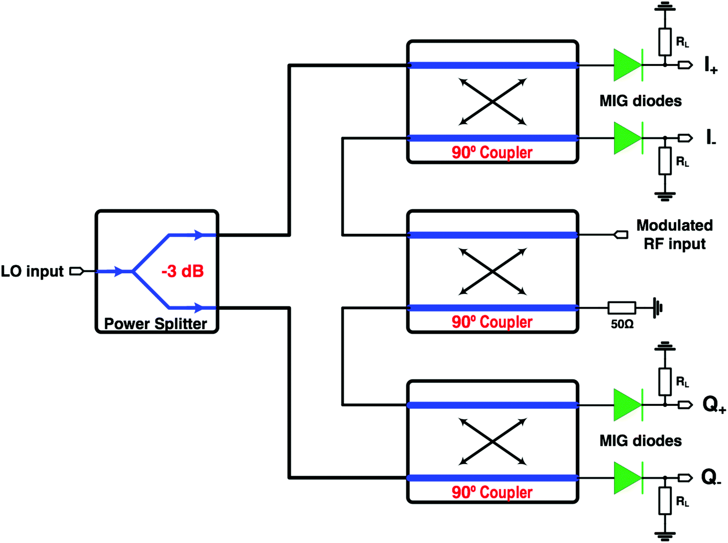 | ||
| Fig. 2 Proposed solution: schematic diagram of the designed six-port receiver frontend showing the 90° quadrature couplers, the power splitter (divider), and the graphene based power detectors. | ||
Graphene diode power detectors
A metal–insulator–graphene (MIG) diode has been reported by the authors on a high resistivity Si (HRS) substrate, showing excellent figures-of-merit for static operation, including a strong maximum nonlinearity of up to 15, and a large maximum responsivity of up to 26 V−1, outperforming state-of-the-art metal–insulator–metal and MIG diodes.25Exploiting this MIG diode, a linear-in-dB power detector on a glass substrate has been reported by the authors showing a tangential responsivity of up to 168 V W−1 at 2.5 GHz and 15 V W−1 at 60 GHz with a better sensitivity than −50 dBm.26 This promising performance enables the demonstration of the six-port receiver on thin-film substrates at least up to millimetre-wave frequencies.
Six-port RF receiver frontend based on the MIG diode
We demonstrate a fully integrated RF receiver frontend centered at 2.4 GHz with a 600 MHz bandwidth exploiting the MIG diode as a power detector. For the prototype receiver, the MIG diode is fabricated on a 500 μm thick glass substrate according the fabrication steps discussed above. The diode was characterized after all the above steps were complete. The I–V characteristics of the diode are shown in Fig. 3(a), from which, it is clear that the performance was not affected by the backend-of-line (BEOL) MMIC process. The characterisation setup as shown in Fig. 3(b) is employed to measure the single-diode-based power detector responsivity. Measurement is carried out by applying the RF power from a calibrated power source at a frequency and bias point, then the corresponding output DC voltage is recorded. The results indicate a responsivity of 42 V W−1 at 2.45 GHz with an RF sensitivity down to at least −50 dBm at zero bias as shown in Fig. 3(c). | ||
| Fig. 3 MIG diode characterisation: (a) Measured I−V characteristics of the fabricated MIG, (b) responsivity measurement setup at different bias voltages, (c) measured diode responsivity with zero-bias at 2.45 GHz. | ||
For the junction design, lumped-element implementation is employed to design the quadrature couplers and the power splitters to achieve integrability at the frequency range from 2.1 to 2.7 GHz. A stand-alone test cell for the passive six-port junction shown in Fig. 4(a) is fabricated to evaluate the RF performance of the junction.
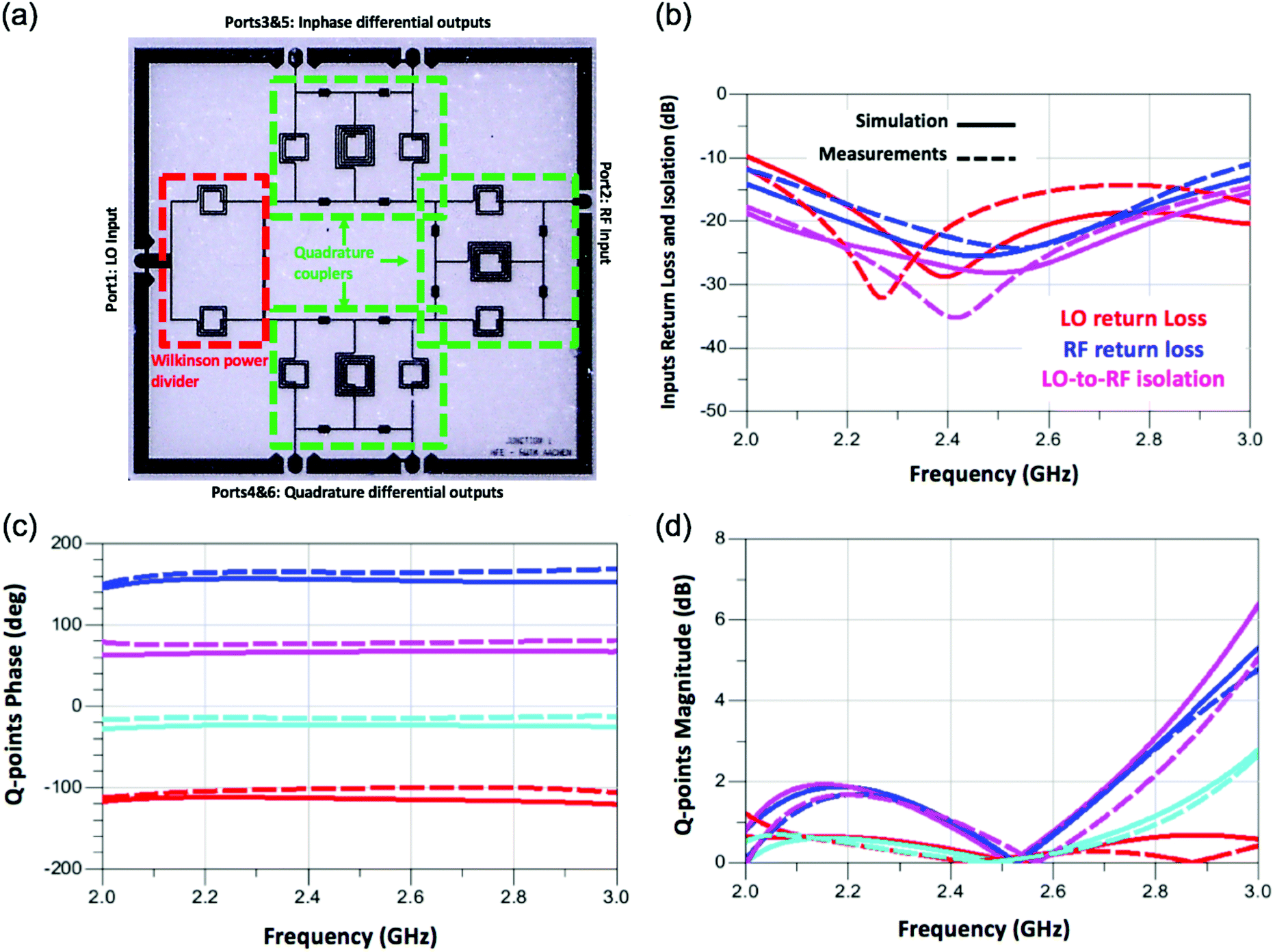 | ||
| Fig. 4 Passive six-port junction characterisation: (a) chip micrograph of the fabricated passive junction occupying 2.3 mm × 1.8 mm chip area, (b) measured and simulated return loss and LO-to-RF isolation of the LO and RF inputs, (c) measured and simulated phases of the four output Q-points, (d) measured and simulated magnitudes of the four output Q-points. | ||
For the passive junction test cell, S-parameter characterisation is performed for the frequency band 2–3 GHz using on-Wafer GSG probes and a standard calibration substrate. Measurement results indicate good matching between the physical electromagnetic (EM) simulations and measurements, demonstrating wideband input matching at both RF and LO ports as shown in Fig. 4(b). A return loss better than −10 dB is measured from 2 to 3 GHz and better than 30 dB LO-to-RF isolation is obtained at 2.45 GHz.
The q-points are the main design measures for the six-port junction, and are expressed as:27
The chip micrograph of the fabricated six-port receiver including the MIG diodes is shown in Fig. 5(a), where four MIG diodes are used with the six-port junction to construct the receiver circuit. 50 Ω brute-force matching resistors are used at the input terminal of the MIG diodes to guarantee a wideband power matching. RF and LO input signals are fed to the circuit through single-ended GSG probing pads while a couple of differential GSSG probing pads are used to extract the receiver IQ baseband output.
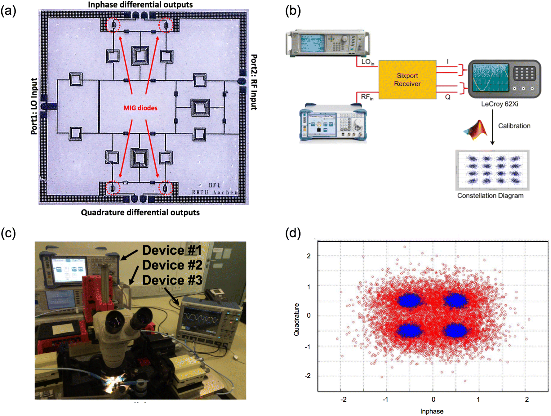 | ||
| Fig. 5 Characterization of the fabricated six-port receiver: (a) chip micrograph of the fabricated prototype six-port receiver including the MIG diode-based power detector occupying 2.3 mm × 2.1 mm chip area, (b) measurement configuration of the graphene-based WiFi receiver frontend including measurement tools and calibration procedure, (c) receiver frontend measurement setup showing the measured differential in-phase signal waveforms, (d) constellation diagram of a QPSK signal before calibration (red) and after calibration (blue). | ||
The prototype receiver is characterized using the block diagram shown in Fig. 5(b) to demodulate a 20 Mbps QPSK signal at 2.45 GHz with −15 dBm modulated RF input power while the LO power was set to 0 dBm. The laboratory setup is shown in Fig. 5(c) with measurement devices listed as follows:
• Device #1: Rohde&Schwarz® vector signal generator used to provide the modulated RF input.
• Device #2: Anritsu® CW generator used to provide the reference LO input.
• Device #3: LeCroy® oscilloscope used to capture the four outputs.
The recorded I and Q data are fed to a MATLAB algorithm for calibration. For calibration, the least squares linearization algorithm is applied to the receiver outputs to linearize the MIG diode for different modulation schemes. Fig. 5(d) shows the measured constellation diagram for the captured I and Q data, before (red) and after (blue) calibration where a significant improvement is achieved. Further improvement could be achieved by adding biasing pads for each MIG diode to enhance the signal sensitivity of the receiver. This helps us to align the performance of the four diodes and compensate fabrication process tolerances; in this way, a more distinguishable constellation diagram could be obtained. In addition, reactive matching can be implemented instead of resistive matching which improves the receiver sensitivity as well as the dynamic range.
Table 2 shows a comparison with the state-of-the-art graphene-based receiver implementations. The presented prototype uses a different implementation method than the conventional architecture used in ref. 14 and 28. It is clear that the proposed architecture not only outperforms the reported state-of-the-art graphene-based receiver, but it also provides the flexibility of implementing the architecture for different frequency ranges and on different substrates. This in turn enables the use of graphene-based circuits and systems for millimetre-wave, and even sub-millimetre-wave frequencies on rigid and flexible substrates for various applications.
Table 3 compares the proposed six-port receivers with other six-port receivers implemented in a relevant frequency range.29–31 Compared to the hybrid implementation reported in ref. 29 and 30, it is clear that the higher bandwidth of the hybrid design has the disadvantage of occupying more chip area. On the other hand, the six-port receiver reported in ref. 31 uses a conventional single stage quadrature coupler which has a lower size but the bandwidth is only 100 MHz. The proposed six-port receiver is the only fully integrated receiver compared to other receivers in this frequency range29–31 achieving a relative bandwidth of 25% centered at 2.4 GHz.
The millimetre-wave receivers reported in ref. 32 and 33 prove that the hybrid implementation is suitable for integration at higher frequencies as shown for the sizes in Table 3. The receiver reported in ref. 32 has been implemented in 0.13 μm CMOS uses MOSFETs as power detectors achieving a relative bandwidth of 6% centered at 62 GHz occupying 1.65 mm × 1.5 mm chip area. The reported size in ref. 32 includes a low noise amplifier (LNA), a voltage controlled oscillator (VCO), a buffer amplifier (BA), an IQ modulator, and a single-pole-double-throw (SPDT) RF switch. The receiver reported in ref. 33 has been implemented in the 0.2 μm GaAs pHEMT process using Schottky diodes as power detectors achieving a relative bandwidth of 15% centered at 65 GHz occupying 3 mm × 2 mm chip area.
Conclusion
Graphene has high potential as an emerging technology not only to introduce devices which can provide a superior performance for frequencies up to submillimetre-waves but also in particular as a candidate for flexible and wearable high frequency electronics due to the substrate independent electrical performance of the graphene field effect transistors. We represent a design approach which enables graphene-based receivers overcoming the limitation of fT and fmax of the graphene transistors in conventional architectures. As a proof-of-concept, we demonstrate for the first time a direct-conversion, full-fledged and fully-integrated RF receiver frontend fabricated on a thin-film glass substrate based on graphene devices suitable for IoT and RFID systems for medical and communication applications.Conflicts of interest
There are no conflicts to declare.Acknowledgements
This work was financially supported by the European Commission under the project Graphene Flagship (contract no. 696656) and the SPINOGRAPH (contract no. 607904) and by the German Science Foundation (DFG) within the priority program 1796 FFlexCom Project GLECS (contract no. NE1633/3).References
- K. S. Novoselov, Science, 2004, 306, 666–669 CrossRef CAS PubMed.
- F. Schwierz, Proc. IEEE, 2013, 101, 1567–1584 CrossRef CAS.
- Y. Wu, X. Zou, M. Sun, Z. Cao, X. Wang, S. Huo, J. Zhou, Y. Yang, X. Yu, Y. Kong, G. Yu, L. Liao and T. Chen, ACS Appl. Mater. Interfaces, 2016, 8, 25645–25649 CAS.
- M. E. Ramón, K. N. Parrish, S. F. Chowdhury, C. W. Magnuson, H. C. P. Movva, R. S. Ruoff, S. K. Banerjee and D. Akinwande, IEEE Trans. Nanotechnol., 2012, 11, 877–883 CrossRef.
- O. Habibpour, Z. S. He, W. Strupinski, N. Rorsman, T. Ciuk, P. Ciepielewski and H. Zirath, IEEE Electron Device Lett., 2016, 37, 333–336 CrossRef CAS.
- J. S. Moon, H.-C. Seo, K.-A. Son, B. Yang, D. Le, H. Fung and A. Schmitz, Microwave Symposium Digest, 2009. MTT '09, IEEE MTT-S International, 2015, pp. 1–4.
- O. Habibpour, S. Cherednichenko, J. Vukusic, K. Yhland and J. Stake, IEEE Electron Device Lett., 2012, 33, 71–73 CrossRef CAS.
- J. S. Moon, H. C. Seo, M. Antcliffe, D. Le, C. McGuire, A. Schmitz, L. O. Nyakiti, D. K. Gaskill, P. M. Campbell, K. M. Lee and P. Asbeck, IEEE Electron Device Lett., 2013, 34, 465–467 CrossRef CAS.
- H. Lyu, H. Wu, J. Liu, Q. Lu, J. Zhang, X. Wu, J. Li, T. Ma, J. Niu, W. Ren, H. Cheng, Z. Yu and H. Qian, Nano Lett., 2015, 15, 6677–6682 CrossRef CAS PubMed.
- O. Habibpour, Z. S. He, W. Strupinski, N. Rorsman, T. Ciuk, P. Ciepielewski and H. Zirath, IEEE Microw. Wirel. Compon. Lett., 2017, 27, 168–170 CrossRef.
- Y. Zhang, M. A. Andersson and J. Stake, 2016 IEEE MTT-S International Microwave Symposium (IMS), 2016, pp. 1–4.
- O. Habibpour, M. Winters, N. Rorsman and H. Zirath, 2014 44th European Microwave Conference, 2014, pp. 371–373.
- M. A. Andersson, O. Habibpour, J. Vukusic and J. Stake, Electron. Lett., 2012, 48, 861–863 CrossRef CAS.
- S.-J. Han, A. V. Garcia, S. Oida, K. A. Jenkins and W. Haensch, Nat. Commun., 2014, 5, 1–6 Search PubMed.
- X. Li, Y. Zhu, W. Cai, M. Borysiak, B. Han, D. Chen, R. D. Piner, L. Colombo and R. S. Ruoff, Nano Lett., 2009, 9, 4359–4363 CrossRef CAS PubMed.
- M. Shaygan, M. Otto, A. A. Sagade, C. A. Chavarin, G. Bacher, W. Mertin and D. Neumaier, Ann. Phys., 2017, 306, 1600410 CrossRef.
- G. F. Engen, IEEE Trans. Microw. Theory Tech., 1977, 25, 1075–1080 CrossRef.
- J. Li, R. G. Bosisio and K. Wu, IEEE Trans. Microw. Theory Tech., 1995, 43, 2766–2772 CrossRef.
- A. O. Olopade, A. Hasan and M. Helaoui, IEEE Trans. Microw. Theory Tech., 2013, 61, 4252–4261 CrossRef.
- A. O. Olopade and M. Helaoui, J. Electr. Comput. Eng., 2014, 2014, 1–7 CrossRef.
- A. Hasan, M. Helaoui, N. Boulejfen and F. M. Ghannouchi, 2015 IEEE Topical Conference on Wireless Sensors and Sensor Networks (WiSNet), 2015, pp. 17–19.
- K. Staszek, S. Gruszczynski and K. Wincza, IEEE Trans. Microw. Theory Tech., 2016, 1–13 CrossRef.
- J.-A. Hou and Y.-H. Wang, IEEE Microw. Wirel. Compon. Lett., 2007, 17, 595–597 CrossRef.
- K. Haddadi and T. Lasri, IEEE Trans. Microw. Theory Tech., 2012, 60, 574–581 CrossRef.
- M. Shaygan, Z. Wang, M. S. Elsayed, M. Otto, G. Iannaccone, A. H. Ghareeb, G. Fiori, R. Negra and D. Neumaier, Nanoscale, 2017, 9, 11944–11950 RSC.
- M. Saeed, A. Hamed, R. Negra, M. Shaygan, Z. Wang and D. Neumaier, 2017 IEEE MTT-S International Microwave Symposium (IMS), 2017, pp. 1649–1652.
- C. de la Morena-Álvarez-Palencia and M. Burgos-Garcia, Prog. Electromagn. Res., 2011, 116, 1–21 CrossRef.
- M. N. Yogeesh, K. Parish, J. Lee, L. Tao and D. Akinwande, 2014 IEEE/MTT-S International Microwave Symposium - MTT 2014, 2014, pp. 1–4.
- J. J. Yao and S. P. Yeo, IEEE Trans. Microw. Theory Tech., 2008, 56, 493–498 CrossRef.
- H.-S. Lim, W.-K. Kim, J.-W. Yu, H.-C. Park, W.-J. Byun and M.-S. song, IEEE Microw. Wirel. Compon. Lett., 2007, 17, 394–396 CrossRef.
- H. L. Lee, D.-H. Park, H.-S. Jang, H.-J. Dong, M.-Q. Lee and J.-W. Yu, 2013 Asia Pacific Microwave Conference - (APMC 2013), 2013, pp. 987–989.
- C. H. Wang, H. Y. Chang, P. S. Wu, K. Y. Lin, T. W. Huang, H. Wang and C. H. Chen, 2007 IEEE International Solid-State Circuits Conference, Digest of Technical Papers, 2007, pp. 192–596.
- T. Brabetz and V. F. Fusco, Gallium Arsenide applications symposium. GAAS 2003, 2003.
Footnote |
| † These authors contributed equally to this work. |
| This journal is © The Royal Society of Chemistry 2018 |