
h-BN/graphene van der Waals vertical heterostructure: a fully spin-polarized photocurrent generator
Xixi
Tao
ab,
Lei
Zhang
 *cde,
Xiaohong
Zheng
*abd,
Hua
Hao
a,
Xianlong
Wang
ab,
Lingling
Song
f,
Zhi
Zeng
ab and
Hong
Guo
dg
*cde,
Xiaohong
Zheng
*abd,
Hua
Hao
a,
Xianlong
Wang
ab,
Lingling
Song
f,
Zhi
Zeng
ab and
Hong
Guo
dg
aKey Laboratory of Materials Physics, Institute of Solid State Physics, Chinese Academy of Sciences, Hefei 230031, China. E-mail: xhzheng@theory.issp.ac.cn
bUniversity of Science and Technology of China, Hefei 230026, China
cState Key Laboratory of Quantum Optics and Quantum Optics Devices, Institute of Laser Spectroscopy, Shanxi University, Taiyuan 030006, China. E-mail: zhanglei@sxu.edu.cn
dDepartment of Physics, Center for the Physics of Materials, McGill University, Montreal, Quebec H3A 2T8, Canada
eCollaborative Innovation Center of Extreme Optics, Shanxi University, Taiyuan 030006, China
fSchool of Electronic Science and Applied Physics, Hefei University of Technology, Hefei 230009, China
gSchool of Physics and Energy, Shenzhen University, Shenzhen 518060, China
First published on 15th November 2017
Abstract
By constructing transport junctions using graphene-based van der Waals (vdW) heterostructures in which a zigzag-edged graphene nanoribbon (ZGNR) is sandwiched between two hexagonal boron-nitride sheets, we computationally demonstrate a new scheme for generating perfect spin-polarized quantum transport in ZGNRs by light irradiation. The mechanism lies in the lift of spin degeneracy of ZGNR induced by the stagger potential it receives from the BN sheets and the subsequent possibility of single spin excitation of electrons from the valence band to the conduction band by properly tuning the photon energy. This scheme is rather robust in that we always achieve desirable results irrespective of whether we decrease or increase the interlayer distance by applying compressive or tensile strain vertically to the sheets or shift the BN sheets in-plane relative to the graphene nanoribbons. More importantly, this scheme overcomes the long-standing difficulties in traditional ways of using solely electrical field or chemical modification for obtaining half-metallic transport in ZGNRs and thus paves a more feasible way for their application in spintronics.
1. Introduction
With the successful fabrication of graphene,1 a hexagonal lattice of carbon atoms with single atom thickness, and the discovery of its many remarkable properties soon afterwards, intensive interest has arisen to investigate other 2D materials. Thus far, many new 2D members, such as hexagonal boron-nitride sheets,2 transition metal dichalcogenides,3 black phospherene,4 borophene,5 2D SiS layers,6 2D silicon carbide (SiC),7–9 and many others,10–14 have been added to the 2D material family. Such 2D materials are considered very important building blocks for future nanoelectronic and optoelectronic devices due to their extraordinary electronic and optoelectronic properties, such as high electron mobility or appropriate band gaps. In parallel with the efforts on continuously discovering new 2D materials, another important research direction on 2D materials has just emerged, which focuses on vertical van der Waals (vdW) heterostructures constructed by stacking different 2D crystals on top of one another.15–24 Since the vdW interaction that binds the stacked layers together is rather weak, the exceptional properties of each layer are well preserved without any degradation. As a matter of fact, the construction of vdW heterostructures has become a very important method for extending the versatility and functionality of 2D materials and finding ways to develop new functions by building heterostructures has attracted more and more interest in the field of 2D materials.25,26It is well known that achieving large spin polarization is an important issue in spintronics and the ultimate goal is to attain fully spin polarized electron conduction in a material or a device. Magnetism is a prerequisite for spin transport. In this regard, among all the 2D materials, graphene is probably the best-known candidate: when cut into nanoribbons, the resulting edges with zigzag geometry configurations have intrinsic edge magnetism arising from localized edge states, unlike most other 2D materials, where magnetism can basically only be induced externally by introducing defects or embedding transition-metal atoms or by other means.27–30 More importantly, quite a few schemes have been suggested to achieve half-metallicity (a property with only one conducting spin channel) in a zigzag edged graphene nanoribbon (ZGNR), such as electrical field,31 edge decoration,32 and B–N co-doping.33,34 These schemes can be divided into two categories: one by applying an electrical field and the other by chemical modification. However, it has been shown that the strength of the electrical field should be extremely high to achieve half-metallicity in ZGNR, which is almost unavailable in the laboratory.35 Meanwhile, with chemical modification it is hard to precisely control the doping or adsorption sites and structural stability. More importantly, as pointed out in our previous work, chemical modification can lead to a dramatic decrease or even the disappearance of the energy difference between the antiferromagnetic (AFM) and ferromagnetic (FM) edge configurations, whereas the half-metallicity can only be obtained from the AFM ground state.36 Thus, a finite temperature can easily turn the ZGNRs paramagnetic, which makes the half-metallicity practically unobservable. Consequently, alternative schemes avoiding the use of either an electrical field or chemical modification for achieving fully spin polarized transport with ZGNRs are greatly anticipated.
In this work, we propose to realize this goal using graphene-based vdW heterostructures. First, a vdW heterostructure h-BN/graphene(Gr)/h-BN is constructed by sandwiching a ZGNR between two hexagonal BN sheets with AA stacking. The stagger potential produced by the two BN sheets at their middle plane acts differently on two sublattices of the ZGNR so that the energies of the edge states with different spins shift oppositely. Thus, the spin degeneracy of the edge states is lifted and two different spin energy gaps Eg↑ and Eg↓ (with Eg↑ < Eg↓) are obtained. Second, linearly polarized light is shed on the central region of a device. By properly tuning the photon energy, electrons with only one spin can be excited from the valence band to the conduction band. Thirdly, through applying a small positive bias in the vdW heterostructure that is smaller than the energy gap Eg↑, the excited electrons in the conduction band can be driven to the right lead, which results in a fully spin polarized photocurrent. This scheme is rather robust in that we can always achieve desirable results irrespective of whether we decrease or increase the interlayer distance by applying compressive or tensile strain vertically to the sheets or shift the BN sheets in-plane relative to the graphene nanoribbon, although the magnitude of the current produced and the photon frequency range needed may vary. Thus, 100% spin polarized transport can always be achieved in graphene/h-BN vdW junctions combined with light irradiation.
2. Theoretical formalism and computational details
The vdW vertical heterostructure device is presented in Fig. 1(a), in which a ZGNR is sandwiched between two zigzag-edged boron-nitride nanoribbons (ZBNNRs). The transport direction is along the z axis and the width of each ribbon in the x direction contains 6 zigzag chains. Each C/B/N atom at the edge is saturated by a H atom. Due to the same hexagonal lattice structure and the very small lattice mismatch (<3%) of the BN sheet (bond length: 1.46 Å) and graphene (bond length: 1.42 Å), the lattice constants of BN ribbons are assumed to be the same as those of the ZGNR. The layers are stacked together by AA stacking which is more favorable in energy than AB stacking.37 The distances between two adjacent layers are relaxed to be 3.22 Å. As shown in Fig. 1(a), the device is divided into three parts: the left lead, the right lead and the central region. The central region consists of 6 unit cells with a length of 14.76 Å including 252 atoms.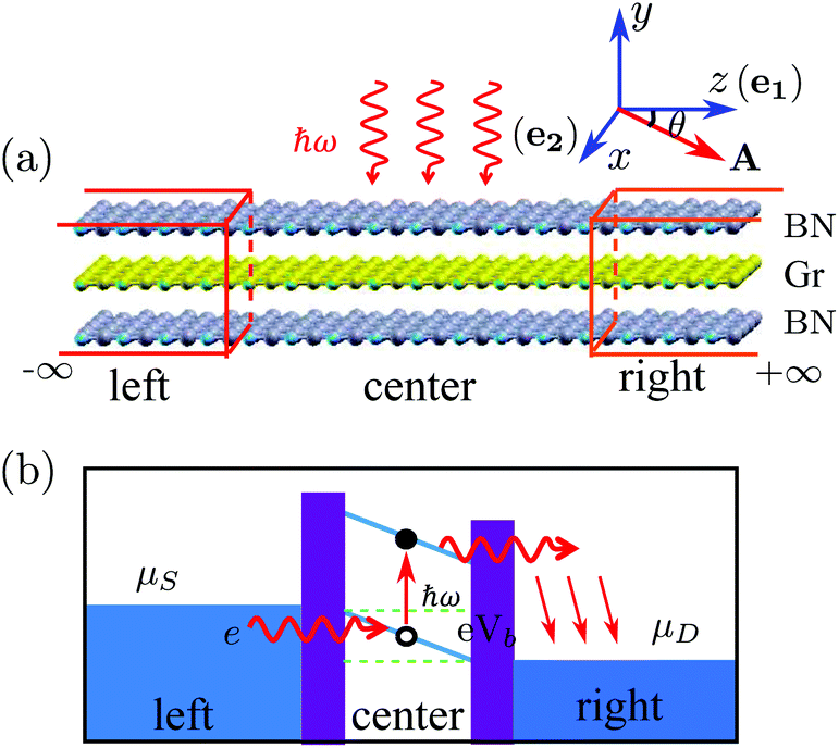 | ||
| Fig. 1 (a) Schematic plot of the vdW vertical heterostructure with a 6-ZGNR (Gr) sandwiched between two 6-ZBNNRs (BN) by AA stacking and it is divided into the left lead, the right lead and the central region where the light impinges. The unit cells of the left and right leads are chosen to be the same, except for a case when discussing the polarization angle effect. The photon has energy ħω. The z axis is along the transport direction and the y axis is perpendicular to the 2D plane of the ribbons. The two vectors e1 and e2 defining the light propagation direction are parallel to the z and x axes respectively. ‘BN’ and ‘Gr’ label the BN sheet and graphene, respectively. A is the electromagnetic vector potential inside the xz plane. (b) The photocurrent generation process. A voltage Vb < Eg↑ is applied between the left lead and the right lead to drive the excited electrons in the conduction band from the central region to the right lead. | ||
In our study, linearly polarized light is shone on the central region with the photon energy and the polarization direction being tunable. A small bias Vb is applied to create a potential drop so that the excited electrons in the conduction band can move unidirectionally from the central region to the right lead. Physically, the photocurrent generation process can be understood as follows (see Fig. 1(b)): the photon excites the valence electron to the conduction band in the central region. Driven by the potential drop, the excited electrons move to the right lead. At the same time, the electrons from the left lead move to the central region to fill the holes left by the previously excited electrons. This process goes on repeatedly and a continuous photocurrent is generated. If the applied bias voltage Vb is smaller than the band gap Eg, the electrical current will only have the photocurrent component, with no direct contribution from the bias.
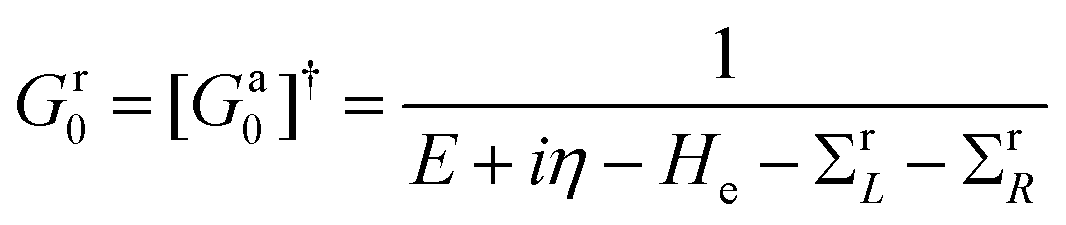
The studied system can be described by the Hamiltonian H = He + He–ph, where He is the Hamiltonian of the two-probe system without the electron–photon interaction and 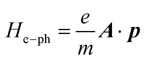 is the electron–photon interaction treated as a perturbation by the first Born approximation.38A is the electromagnetic vector potential and p is the momentum of the electron. As a matter of fact, the calculation of the photocurrent is a kind of post-analysis, which means that we will neglect the effect of He–ph during the self-consistent first-principles calculation and the Hamiltonian part of He–ph is treated as the perturbation after self-consistent Hamiltonian He is obtained. Then, the effective transmission function can be expressed in terms of Green's function39
| Tα,s(E) = Tr{Γα,s(E)[(1 − fα(E))G<s(E) + fα(E)G>s(E)]}, | (1) |
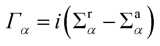 (α = L, R) is the linewidth function describing the coupling between the central region and both leads, with
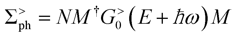
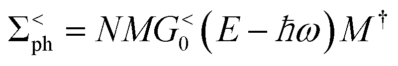
  being the self-energy of the semi-infinite α-th lead. fα is the Fermi–Dirac distribution of the α-th electron reservoir. G</> = G0</> + Gph</> is the lesser/greater Green's function of the central region which takes account of the self-energies of both leads as well as the electron–photon interaction,
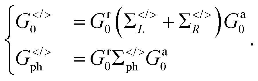 | (2) |
It means that the effective transmission has two contributions, with the first one directly coming from the voltage and the other solely from photons. The retarded and advanced Green's functions in eqn (2) are defined as
 | (3) |
 | (4) |
 | (5) |
| Mnm = 〈n|A0ê·p|m〉, | (6) |
| ê = cos(θ)e1 + sin(θ)e2, | (7) |
The self-consistent calculations for He were performed combining density functional theory (DFT) with the nonequilibrium Green's function (NEGF) method for a quantum transport study,42,43 as implemented in the Nanodcal package,44 in which norm-conserving pseudopotentials and linear combinations of atomic orbitals as basis sets are adopted. The wave function is expanded with a double zeta polarized (DZP) basis set and the fineness of the real space grid is determined by an equivalent plane wave cutoff of 200 Ry. The exchange-correlation potential was treated at the level of generalized gradient approximation (GGA), using the functional of Perdew, Burke, Ernzerhof (PBE). The structure relaxation is performed over a smallest repeated unit cell by a conjugate gradient method until the residual force on each atom is less than 0.04 eV Å−1. The convergence criterion of electronic self-consistent calculations is set as 1 × 10⁻⁴a.u. for both the Hamiltonian matrix and the density matrix. The k-point sampling grid for both structure relaxation and the lead part of transport calculation is chosen as 1 × 1 × 100.
The spin polarized current can be calculated by integrating the effective transmission function39
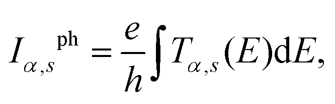 | (8) |
3. Results and discussion
At the beginning, we calculate the band structures of the single ZGNR and the h-BN/Gr/h-BN structure (see Fig. 2(a) and (b)) to see the electronic structure difference between a pristine graphene nanoribbon and a vdW heterostructure. In the ground state, the two edges of the single ZGNR are anti-ferromagnetically (AFM) coupled. The magnetic moments of edge carbon atoms at the two edges are 0.29μB and −0.29μB, respectively. Note that the band structure of ZGNR is spin degenerate with a band gap of 0.63 eV (see Fig. 2(a)). Thus, for such an isolated ZGNR, photon irradiation with a certain photon energy ħω > 0.63 eV will excite electrons of both spins from the valence band to the conduction band and thus will generate a photocurrent with no spin polarization. In contrast, as shown in Fig. 2(b), the spin degeneracy is broken in the h-BN/Gr/h-BN vdW heterostructure. The band gap for spin up electrons is decreased to Eg↑ = 0.28 eV while that for spin down electrons is increased to Eg↓ = 0.82 eV. The energy gap at the X point changes from 0.95 eV to 0.50 eV and 1.15 eV for spin up and spin down, respectively. It is important to notice this for a later discussion of the photocurrent generation. Due to the existence of the BN sheets and the subsequent broken symmetry, the maximum magnetic moments of the edge carbon atoms decrease slightly and unequally to 0.28 and −0.26 μB, respectively. | ||
| Fig. 2 The band structure of: (a) single layer ZGNR and (b) the h-BN/Gr/h-BN vdW vertical heterostructure. The numbers are the real energy gap values and those at the X point. The effective potential at the graphene plane produced by: (c) two BN nanoribbons and (d) two infinite BN layers. ‘B’ and ‘N’ indicate the CB and CN sites in graphene. | ||
Next, we will discuss the physics behind the spin degeneracy lift in the h-BN/Gr/h-BN system. There are two sublattices in both graphene and BN sheets. With AA stacking, if we view the system from top to bottom, the atoms of one sublattice in graphene overlap with the B atoms in the BN sheets and those of the other sublattice overlap with the N atoms. Thus, the two sublattices in graphene can be labelled as CB and CN, respectively (see Fig. 3). The existence of the BN sheets will produce a potential, which will influence the electronic structure of the graphene nanoribbon. Since each CB atom is between two B atoms and each CN atom is between two N atoms, they will experience different local potentials produced by the BN sheets. To see the potential difference, we extracted the local potentials around each CB and CN atom by averaging around each site in a certain radius, which are shown in Fig. 2(c). The potential is obtained by artificially taking away the graphene layer with the positions of the BN sheets fixed. Clearly, the potential at each CB site is much smaller than those at the neighboring CN sites. Note that the potentials at the CB sites (or CN sites) are non-uniform due to the existence of boundaries and structure asymmetry. For infinite BN layers, the potential at each CB site (or CN) is exactly the same (see Fig. 2(d)).
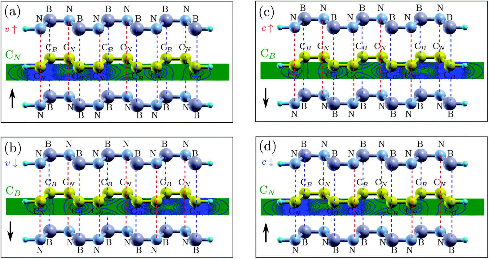 | ||
| Fig. 3 The vdW structure and the edge states of the ZGNR for: (a) spin up in the valence band (v↑); (b) spin down in the valence band (v↓); (c) spin up in the conduction band (c↑); and (d) spin down in the conduction band (c↓). CB and CN indicate the carbon atoms in the two sublattices. In each panel, at the left border, the CB or CN in green indicates that the edge state is distributed at the CB or CN sublattice and the arrow at the down-left corner indicates the increase or the decrease of energy of the edge states. The edge states are obtained by calculation for a single ZGNR. | ||
Consequently, the BN sheets produce a stagger potential at the ZGNR plane, which is larger at the CN sublattice and smaller at the CB sublattice. Interestingly, we find that, in the ZGNR, the spin up edge states of the valence band are distributed only at the CN sublattice and localized at the left edge (see Fig. 3(a)) while the spin down edge states of the valence band are only distributed at the CB sublattice and localized at the right side (see Fig. 3(b)). Thus, the energy of the spin up edge state will be shifted up (close to the Fermi level) while that of the spin down edge state will be shifted down (away from the Fermi level). Likewise, in the conduction band, the spin up edge states are only distributed at the CB sublattice (see Fig. 3(c)) while the spin down edge states are only distributed at the CN sublattice (see Fig. 3(d)), which result in the energy of the spin up edge states shifting down (close to the Fermi level) and that of the spin down edge states shifting up (away from the Fermi level). Overall, the spin up edge states in both the valence and conduction bands shift close to the Fermi level while the spin down edge states move farther from it, resulting in the breaking of spin degeneracy (see Fig. 2(b)).
Having understood the spin splitting in the bandstructure of the h-BN/Gr/h-BN vdW vertical heterostructure, we now investigate the generation of a fully spin polarized photocurrent out of this vdW heterostructure. Generally speaking, a stable photocurrent can be directly generated by light irradiation without an external bias in two kinds of devices. One is based on the PN junction41 and the other is a system with a lack of space inversion symmetry.45 For other systems, a small bias should be applied to the device to create a potential drop along which the photon-excited electrons in the conduction band can move unidirectionally toward one electrode.39 In our study, a linearly polarized light with photon energy ħω is shed on the central region. The polarization direction (the direction of magnetic vector potential A) in eqn (7) is chosen by taking e1 along the z axis, e2 along the x axis, and θ = 0° (see Fig. 1(a)). Considering the different spin band gaps (0.28 eV for spin up and 0.82 eV for spin down), we chose a bias voltage of 0.25 V, which will not produce a DC current directly between the two electrodes and the detected current in the device must be generated by photons. The photocurrent as a function of the photon energy ħω is presented in Fig. 4(a). It is interesting to see that when the photon energy ħω > 0.0 and ħω < 0.60 eV, the spin up component of the photocurrent I↑ph ≠ 0 while the spin down component of the photocurrent I↓ph = 0, producing a 100% spin polarized photocurrent.
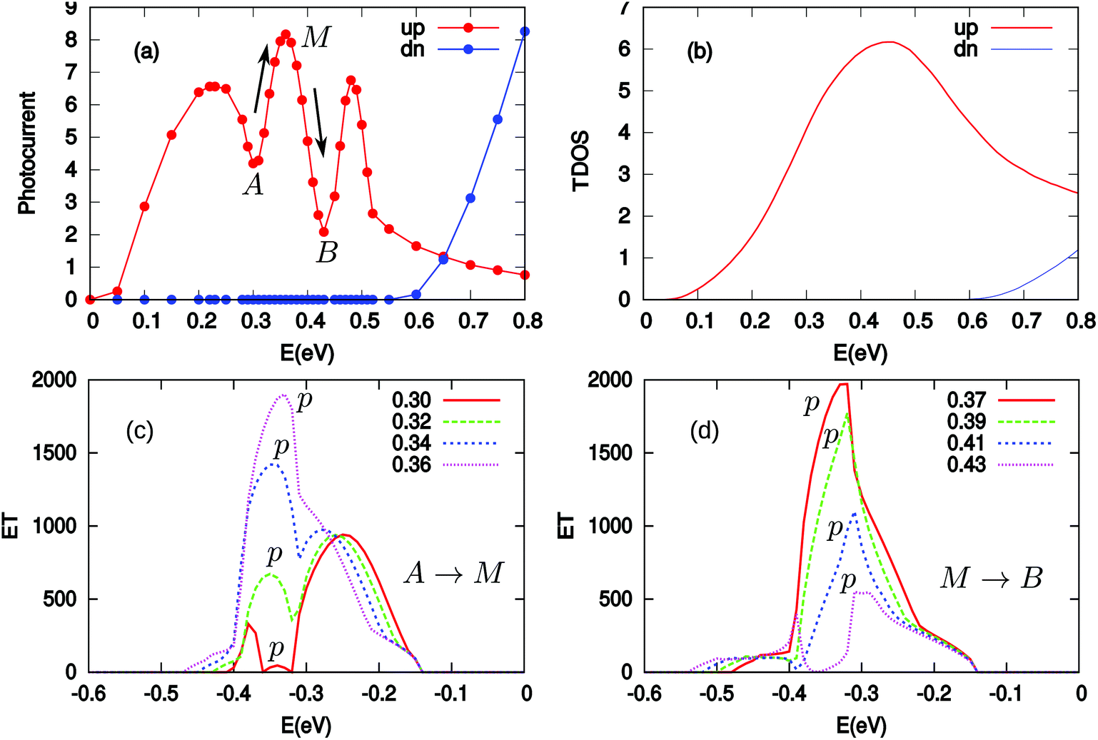 | ||
| Fig. 4 (a) Two spin components of the photocurrent (Iphα,s with α = L, s = ↑ and ↓) versus the photon energy (E = ħω) when a bias voltage of 0.25 V is applied in the system; (b) the transition density of states (TDOS) as a function of photon energy E; (c) and (d) the evolution of effective transmission (ET) function with the increase of photon energy for A → M and M → B stages, respectively. | ||
In the following, we will further discuss three facts presented in Fig. 4(a): (1) the spin up photocurrent starts almost at ħω = 0.0 eV; (2) the spin down photocurrent starts when ħω > 0.55 eV; and (3) the spin up photocurrent starts decreasing from 0.50 eV monotonously. To understand these features, we plot a cartoon figure for the tilting of the edge state band structure in the central region without and with the application of a bias (see Fig. 5). When Vb = 0, an electron can only be excited from the valence band to the conduction band when the photon energy ħω ≥ Eg (see Fig. 5(a)). However, when a bias voltage Vb is applied, the band structure gets tilted, that is, the energy of the states at the left side increases while that at the right side decreases (see Fig. 5(b)). The electrons at the up-left corner (see the blue triangle) in the valence band can be excited to the down-right corner (also see the blue triangle) of the conduction band by photons with much smaller energy. The minimum energy is determined by the excitation process from v0 to c3. For the spin up photocurrent, the starting energy ħω = Eg↑ − Vb = 0.28 − 0.25 = 0.03 eV. This is the reason that the spin up photocurrent starts almost at 0.0 eV when a bias of 0.25 V is applied. With the increase of ħω, more and more electrons in the blue triangle area (larger area) in the valence band will be excited to the blue triangle area in the conduction band (see Fig. 5(b)). Thus we see an increase in this region starting from 0 in the photocurrent. The same trend is observed for the spin down photocurrent, but the threshold energy will be ħω = Eg↓ − Vb = 0.82 − 0.25 = 0.57 eV. That is why the spin down photocurrent starts appearing when ħω > 0.55 eV. For the spin up component, since the energy difference between v1 and c1 is 0.50 eV (the band gap value at the X point in Fig. 2(b)), when ħω = 0.50 eV, all the electrons in the states above v1 in the valence band cannot be excited into an available empty state in the conduction band; thus the excitation will be suppressed. At this time, all the states in the red dot-dashed triangle area crossing v1 in the valence band can find an empty state in the red dot-dashed triangle area crossing c2 in the conduction band to induce an excitation. With the increase of ħω, these two triangle areas for generating the photocurrent become smaller and smaller (see the green triangle area at down-right and up-left corners in Fig. 5(b)), which leads to the decrease of the photocurrent.
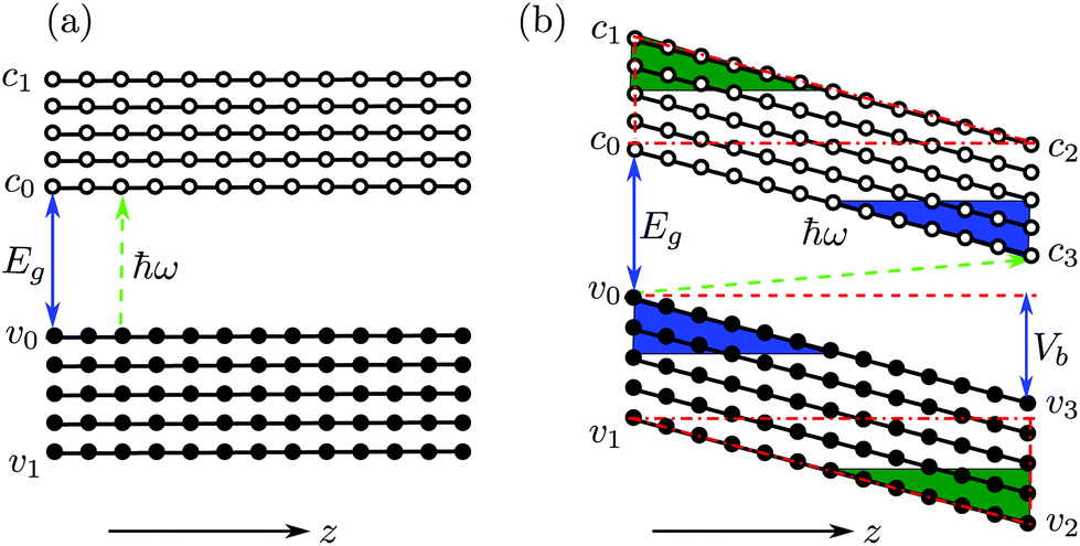 | ||
| Fig. 5 A cartoon of the band profile of the edge states: (a) at equilibrium and (b) at a finite bias (Vb). The filled circles indicate the valence bands and the corresponding edge states while the empty circles indicate the conduction band and its corresponding edge states. In (b), v0 − v3 (c0 − c3) are four boundary points or states in the valence (conduction) band. Vb is the applied bias and Eg is the band gap. Green arrow indicates an excitation process between an edge state pair induced by a photon (ħω). z is along the transport direction. | ||
It is interesting to note the oscillations between 0.20 and 0.50 eV. There are three peaks (with the middle one labelled as “M”) and two valleys (labelled as “A” and “B”). In order to understand these peaks and valleys, we calculated the transition density of states (TDOS). We use Ehv to describe the energy of state h in the valence band and Eic to describe the energy of state i in the conduction band. When the band structure in the central region is tilted under a bias of 0.25 V, the energy of any state at different z (the position along the transport direction) will be  for the valence band and
 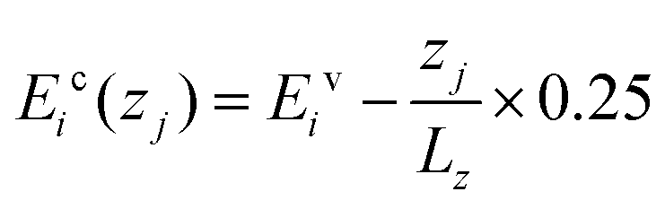 for the conduction band, where zj or zk is the position along the z direction and Lz is the length of the central region. We may use a combination index hk to specify the state h in the valence band at positions k and ij to specify the state i in the conduction band at position j. A photon with energy ħωhk,ij = Eic(zj) − Ehv(zk) can always find a pair of initial state hk and a final state ij between which it could excite an electron. The TDOS is defined as
  . The TDOS including the contribution from both the edge states and the bulk states is shown in Fig. 4(b). For the spin up channel, the overall profile in the TDOS and the photocurrent are approximately the same. This demonstrates the great importance of TDOS in generating the photocurrent. However, we also have to note that the TDOS consists of only one large smooth peak while the photocurrent contains fine structures with three narrower peaks. This indicates that the TDOS is not the only factor determining the photocurrent. Actually, the transition rate between different initial–final (hk − ij) state pairs may vary greatly. We calculated the effective transmission function as a function of valence electron energy corresponding to each photon energy studied in the photocurrent in Fig. 4(a). The effective transmission function is very important in understanding the photocurrent. On one hand, it directly reflects the transition rate at each valence electron energy under different photon energies. On the other hand, its integration leads to the photocurrent according to eqn (8). As an example, we will show the evolution of the effective transmission function with the photon energy increasing from valley A to peak M and then from peak M to valley B. They are shown in Fig. 4(c) and (d), respectively. We clearly see that for different photon energies, the effective transmission function and thus the transition rate are greatly different. We find for both the A → M stage and the M → B stage that the energy range for the excited valence electrons increases with the increase of photon energy. Meanwhile, in the A → M stage, there is a peak p increasing with the photon energy, which leads to the increase of the photocurrent. In contrast, in the M → B stage, the main peak p shrinks with photon energy, which leads to the decrease of the photocurrent.
The maximum energy range for the edge states determined by the energy difference between v1 and c2 is 0.75 eV. This can be understood as follows: from Fig. 2(b), we see that the band gap of spin up is 0.28 eV. This is the lowest photon energy that can be used to excite electrons when no bias is applied. However, also notice the gap of 0.5 eV at the X point. It is the largest photon energy that can be used to excite electrons from the edge states in the valence band to the edge states in the conduction band. However, when the band structure of the central region is tilted by a 0.25 V bias (see Fig. 5(b)), the largest photon energy for exciting electrons from the edge states in the valence band to the edge states in the conduction band, namely, from the state at v2 to the state at c1, will be 0.75 eV (0.50 + 0.25 = 0.75). If the photon energy is larger than 0.75 eV, no transition between edge states will occur. However, when ħω > 0.75 eV, the current can still be contributed by the transition between the bulk states located at the left part (G-A section) in the band structure shown in Fig. 2(b) and this is why we can still see a finite photocurrent when ħω > 0.75 eV for the spin up channel. It is worth mentioning that there is also a contribution from the bulk states in the 0.0–0.75 eV range.
From the discussion above, we see that the bias voltage plays an important role in the generation of photocurrent, and especially it directly affects the threshold of photon energy. It will be very interesting to know how it changes the magnitude of the photocurrent. For doing so, we fix the photon energy ħω = Eg,↑ = 0.28 eV and increase the bias voltage from 0.05 V to 0.25 V. The effective transmission function is presented in Fig. 6(a). It is seen that with the increase of the bias, the electrons in a larger energy range in the valence band can be excited to the conduction band and thus contribute to the photocurrent. This can be easily understood. When Vb = 0.05 V, the band structure in the central region is very slightly tilted, which can still be approximated by Fig. 5(a). Only the electrons at the valence maximum through all the central region can be excited to the conduction minimum. With the increase of the bias, the band structure will be much more tilted; thus, electrons with lower energy can be excited. The width of the energy range of the excited electrons is exactly the magnitude of the applied bias. However, even though the energy range of the excited electrons is increased, the photocurrent is decreased (see Fig. 6(b)), which should arise from the decreased density of states at each energy and the decreased transition probability under a higher bias.
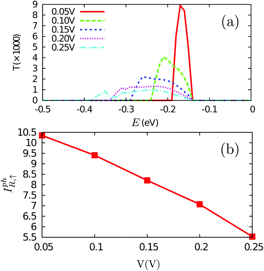 | ||
| Fig. 6 The bias dependence of: (a) the effective transmission function and (b) the photocurrent in the right lead (‘R’). The photon energy ħω is fixed as 0.28 eV. In (a), E is the energy of the electrons excited in the valence bands. Only spin up is shown since the contribution of spin down is zero under these conditions. | ||
Proceeding further, we will study the effect of the polarization angle θ. Without the loss of generality, two cases are considered: (A) Vb = 0.25 V and ħω = 0.20 eV; (B) Vb = 0.25 V and ħω = 0.10 eV. The Iαph(θ) as a function of θ is shown in Fig. 7 (see the curves labelled as ‘A’ and ‘FA’, ‘B’ and ‘FB’). It is clear that both of them satisfy a cosine relationship with the period T = π. To understand it, with some derivation starting from eqn. (1) to (8), we have (with the spin index omitted):
 | (9) |
 | (10) |
 | (11) |
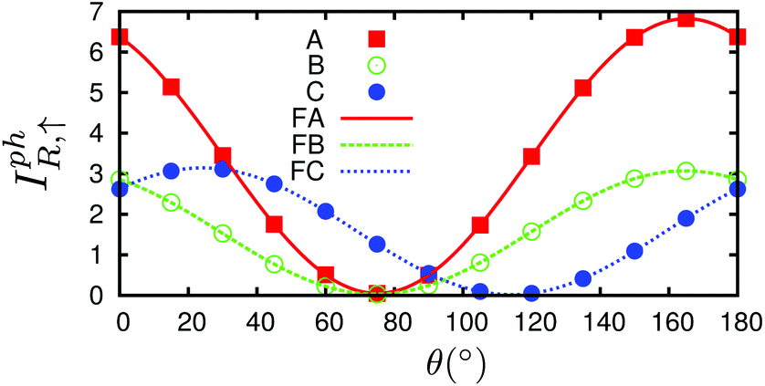 | ||
| Fig. 7 The dependence of the photocurrent on polarization angle θ of three cases: (a) Vb = 0.25 V and ħω = 0.20 eV, labelled as ‘A’ and ‘FA’; (b) Vb = 0.25 V and ħω = 0.10 eV, labelled as ‘B’ and ‘FB’; (c) Vb = 0.25 V and ħω = 0.10 eV and the central region has a mirror symmetry, labelled as ‘C’ and ‘FC’. ‘A’, ‘B’ and ‘C’ are the calculated data while ‘FA’, ‘FB’ and ‘FC’ are the corresponding fitted curves. Only spin up is nonzero and shown. | ||
It is seen that, the photocurrent is highly dependent on the polarization angle and can be switched on and off by tuning θ. The maximum/minimum photocurrent will be 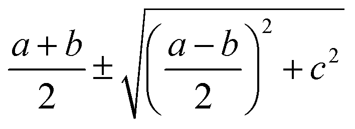 . We see that θ = 0, which means A//z, does not correspond to a maximum photocurrent, but there is a phase shift of 2ϕ0. By fitting, we get Iαph = 3.39 × cos(2θ + 30.0) + 3.44 for case (A) and Iαph = 1.52 × cos(2θ + 30.0) + 1.55 for case (B). Thus ϕ0 ≃ 15.0° for these cases.
This phase shift is basically not caused/changed by the photon energy as seen, but by the asymmetry of the system, which can arise either from the structure asymmetry or from the bias. The bias induced asymmetry directly arises from the charge redistribution due to the bias and the subsequent asymmetrical potential profile. To prove that the bias can also cause the phase shift, we considered a third case (C) in which the central region is symmetrical by choosing the left and right leads with mirror symmetry. For Vb = 0.25 V and ħω = 0.10 eV, a phase shift is still seen from curve ‘C’ in Fig. 7. By fitting, we have Iαph = 1.56 × cos(2θ − 48.0) + 1.58; thus ϕ0 ≃ −24.0°. In a system with left–right symmetry studied by Xie et al., namely, zigzag edged monolayer black phospherene nanoribbon doped with sulfur atoms, where both structural asymmetry and bias effect are absent and the photocurrent induced by linearly polarized light is totally caused by the photogalvanic effects, the phase shift is exactly zero.45 In addition, from the three fitting expressions above we know that the photocurrent Iαph will always be larger than zero, thus flowing to the right lead, due to the bias polarity applied.
Finally, to investigate the robustness of the full spin polarization of the photocurrent, we considered several factors that may lead to the changes of the geometry structures. We are mainly concerned with the effects of the vertical strain and the in-plane relative shift on the photocurrent. To be specific, we considered four cases: (1) an increase of the layer distance by 0.30 Å(+9.3%); (2) a decrease of the layer distance by 0.30 Å(−9.3%); (3) a shift of half a unit cell along the transport direction; and (4) AB stacking. We consider the first two cases since strain or pressure has become an important means for property and function tuning in the material or device design and we consider the last two cases since they may also appear in real situations although their structures are not the most stable. Especially, in practice, some degree of misalignment between the sheets would exist. The last two cases are typical ones which can give us information on effects of such misalignment. Since the spin polarization of the photocurrent is largely determined by the spin splitting of the band structure, for qualitative discussions, it is sufficient to analyze the band structure changes in these cases (see Fig. 8). It is seen that in all these cases, large spin splitting is always obtained. Especially, the change in the layer distance greatly affects the band structure. When it is increased by 0.30 Å, the band gap is increased to 0.46 eV and 0.73 eV for spin up and spin down, respectively (see Fig. 8(a)). Meanwhile, when the distance is decreased by 0.30 Å, the band gap for spin up is almost closed (0.06 eV) while that for spin down is increased to 0.88 Å (see Fig. 8(b)). This is because the smaller the layer distance, the larger the local potential difference between the CB and CN sublattices that will be produced, which increases the energy differences of the edge states of different spins. In the two cases of in-plane shift, which are two second most stable structures, besides the AA stacking that we previously investigated, large spin splitting is still observed and they show almost equal band gaps for each spin (see Fig. 8(c) and (d), 0.53 and 0.51 eV for spin down while 0.75 and 0.71 eV for spin up). However, in case (3), after the shift, the CB atoms are much closer to the N atoms than the B atoms while the CN atoms are much closer to the B atoms, which leads to the increase of the band gap of spin up and the decrease of spin down, that is, spin down has a smaller band gap (see Fig. 8(c)). In the AB stacking shown in Fig. 8(d), the CB atoms are right below (above) the N atoms while the CN atoms are right below (above) the hexagon center; thus the spin up band gap is increased while the spin down band gap is decreased. Since the potential difference of the CB and CN sublattices in these two cases is smaller than the AA stacking, the spin splitting is also smaller. Therefore, a fully spin polarized photocurrent can always be achieved, although the required photon energy range and the produced photocurrent magnitude may be different.
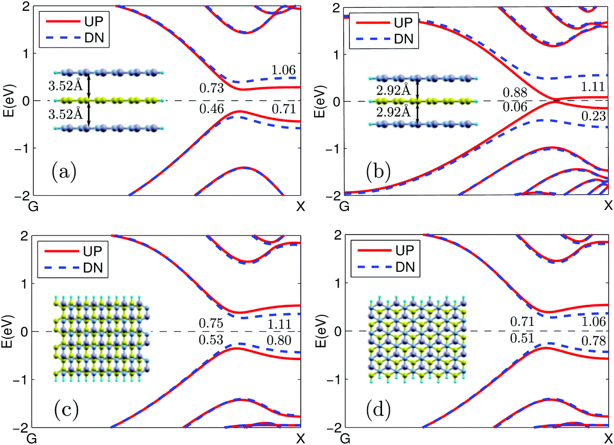 | ||
| Fig. 8 The band structure for the cases in which: (a) the layer distance is increased by 0.30 Å; (b) the layer distance is decreased by 0.30 Å; (c) the ZGNR is shifted along the transport direction by half a unit cell and (d) the ZGNR is shifted along the x direction to make an AB stacking. | ||
4. Conclusion
In summary, we have proposed a h-BN/Gr/h-BN vdW heterostructure for generating a fully spin polarized photocurrent. Due to the stagger potential produced by the BN sheets, the two sublattices of the graphene nanoribbon experience different potentials imposed by the BN nanoribbons, which causes a shift of the energy of the edge states with different spins towards opposite directions. This results in the spin splitting of the band structure and makes single spin excitation possible by properly selecting the photon energy. Besides the most stable AA stacking structure, our systematic study of the other four cases changing the relative positions of the BN sheets to the graphene ribbons indicates that the fully spin polarized current can always be achieved, although the photon energy range that can be used will be different. Note that, compared with the electrical or chemical ways for achieving fully spin polarized transport with graphene, the idea of the vertical Gr/h-BN vdW heterostructure is more practical since it can be easily fabricated by a lot of schemes, such as mechanical cleavage methods, layer-by-layer transfer techniques, co-segregation growth, temperature-triggered chemical switching growth or CVD growth.19–21,46,47 In a word, by combining with photon irradiation, our study demonstrates the great importance and potential of 2D vdW heterostructures in spintronics, which should be taken into consideration in the design of spintronic devices based on 2D materials.Conflicts of interest
There are no conflicts to declare.Acknowledgements
We gratefully acknowledge the financial support by the National Natural Science Foundation of China under Grant Nos. 11574318 (X. Z.), 11704232 (L. Z.), 11374301 (H. H.) and 21503061 (L. S.); Shanxi Science and Technology Department (No. 201701D121003) (L. Z.); National Key R&D Program of China under Grants No. 2017YFA0304203 (L. Z.) and No. 2016YFA0301700 (L. Z.); the Fund for Shanxi 1331KSC (L. Z.); the Major/Innovative Program of Development Foundation of Hefei Center for Physical Science and Technology (under Grant No. 2016FXCX003) (X. Z.); and the Natural Sciences and Engineering Research Council of Canada (NSERC) (H. G.). Calculations were performed in Center for Computational Science of CASHIPS, the ScGrid of Supercomputing Center and Computer Network Information Center of Chinese Academy of Sciences.References
- K. S. Novoselov, A. K. Geim, S. Morozov, D. Jiang, Y. Zhang, S. Dubonos, I. Grigorieva and A. Firsov, Science, 2004, 306, 666–669 CrossRef CAS PubMed.
- C. Zhi, Y. Bando, C. Tang, H. Kuwahara and D. Golberg, Adv. Mater., 2009, 21, 2889–2893 CrossRef CAS.
- K. Novoselov, D. Jiang, F. Schedin, T. Booth, V. Khotkevich, S. Morozov and A. Geim, Proc. Natl. Acad. Sci. U. S. A., 2005, 102, 10451–10453 CrossRef CAS PubMed.
- L. Li, Y. Yu, G. J. Ye, Q. Ge, X. Ou, H. Wu, D. Feng, X. H. Chen and Y. Zhang, Nat. Nanotechnol., 2014, 9, 372–377 CrossRef CAS PubMed.
- A. J. Mannix, X.-F. Zhou, B. Kiraly, J. D. Wood, D. Alducin, B. D. Myers, X. Liu, B. L. Fisher, U. Santiago and J. R. Guest, et al. , Science, 2015, 350, 1513–1516 CrossRef CAS PubMed.
- J. Yang, Y. Zhang, W.-J. Yin, X. Gong, B. I. Yakobson and S.-H. Wei, Nano Lett., 2016, 16, 1110–1111 CrossRef CAS PubMed.
- M. N. Huda, Y. Yan and M. M. Al-Jassim, Chem. Phys. Lett., 2009, 479, 255–258 CrossRef CAS.
- X. Zheng, X. Chen, L. Zhang, L. Xiao, S. Jia, Z. Zeng and H. Guo, 2D Mater., 2017, 4, 025013 CrossRef.
- P. Jiang, X. Tao, H. Hao, L. Song, X. Zheng, L. Zhang and Z. Zeng, 2D Mater., 2017, 4, 035001 CrossRef.
- Y. Ma, Y. Dai, M. Guo, C. Niu, Y. Zhu and B. Huang, ACS Nano, 2012, 6, 1695–1701 CrossRef CAS PubMed.
- D. C. Elias, R. R. Nair, T. M. G. Mohiuddin, S. V. Morozov, P. Blake, M. P. Halsall, A. C. Ferrari, D. W. Boukhvalov, M. I. Katsnelson and A. K. Geim, et al. , Science, 2009, 323, 610–613 CrossRef CAS PubMed.
- D. Malko, C. Neiss, F. Viñes and A. Görling, Phys. Rev. Lett., 2012, 108, 086804 CrossRef PubMed.
- D. D. Vaughn II, R. J. Patel, M. A. Hickner and R. E. Schaak, J. Am. Chem. Soc., 2010, 132, 15170–15172 CrossRef PubMed.
- L.-D. Zhao, S.-H. Lo, Y. Zhang, H. Sun, G. Tan, C. Uher, C. Wolverton, V. P. Dravid and M. G. Kanatzidis, Nature, 2014, 508, 373–377 CrossRef CAS PubMed.
- L. Samad, S. M. Bladow, Q. Ding, J. Zhuo, R. M. Jacobberger, M. S. Arnold and S. Jin, ACS Nano, 2016, 10, 7039 CrossRef CAS PubMed.
- L. Ponomarenko, A. Geim, A. Zhukov, R. Jalil, S. Morozov, K. Novoselov, I. Grigorieva, E. Hill, V. Cheianov and V. Fal'Ko, et al. , Nat. Phys., 2011, 7, 958–961 CrossRef CAS.
- A. Azizi, S. Eichfeld, G. Geschwind, K. Zhang, B. Jiang, D. Mukherjee, L. Hossain, A. F. Piasecki, B. Kabius and J. A. Robinson, ACS Nano, 2015, 9, 4882 CrossRef CAS PubMed.
- L. Britnell, R. Gorbachev, R. Jalil, B. Belle, F. Schedin, A. Mishchenko, T. Georgiou, M. Katsnelson, L. Eaves and S. Morozov, et al. , Science, 2012, 335, 947–950 CrossRef CAS PubMed.
- C. R. Dean, A. F. Young, I. Meric, C. Lee, L. Wang, S. Sorgenfrei, K. Watanabe, T. Taniguchi, P. Kim and K. Shepard, et al. , Nat. Nanotechnol., 2010, 5, 722–726 CrossRef CAS PubMed.
- S. Haigh, A. Gholinia, R. Jalil, S. Romani, L. Britnell, D. Elias, K. Novoselov, L. Ponomarenko, A. Geim and R. Gorbachev, Nat. Mater., 2012, 11, 764–767 CrossRef CAS PubMed.
- Q. Li, M. Liu, Y. Zhang and Z. Liu, Small, 2016, 12, 32–50 CrossRef CAS PubMed.
- T. Georgiou, R. Jalil, B. D. Belle, L. Britnell, R. V. Gorbachev, S. V. Morozov, Y.-J. Kim, A. Gholinia, S. J. Haigh and O. Makarovsky, et al. , Nat. Nanotechnol., 2013, 8, 100–103 CrossRef CAS PubMed.
- A. K. Geim and I. V. Grigorieva, Nature, 2013, 499, 419–425 CrossRef CAS PubMed.
- Y. Liu, N. O. Weiss, X. Duan, H.-C. Cheng, Y. Huang and X. Duan, Nat. Rev. Mater., 2016, 1, 16042 CrossRef CAS.
- H. Sadeghi, S. Sangtarash and C. J. Lambert, 2D Mater., 2017, 4, 015012 CrossRef.
- J. Wong, D. Jariwala, G. Tagliabue, K. Tat, A. R. Davoyan, M. C. Sherrott and H. A. Atwater, ACS Nano, 2017, 11, 7230 CrossRef CAS PubMed.
- O. V. Yazyev and L. Helm, Phys. Rev. B: Condens. Matter Mater. Phys., 2007, 75, 125408 CrossRef.
- W. Hu and J. Yang, J. Phys. Chem. C, 2015, 119, 20474–20480 CAS.
- L. Seixas, A. Carvalho and A. H. Castro Neto, Phys. Rev. B: Condens. Matter Mater. Phys., 2015, 91, 155138 CrossRef.
- A. Krasheninnikov, P. Lehtinen, A. S. Foster, P. Pyykkö and R. M. Nieminen, Phys. Rev. Lett., 2009, 102, 126807 CrossRef CAS PubMed.
- Y. W. Son, M. L. Cohen and S. G. Louie, Nature, 2006, 444, 347 CrossRef CAS PubMed.
- E.-J. Kan, Z. Li, J. Yang and J. G. Hou, J. Am. Chem. Soc., 2008, 130, 4224 CrossRef CAS PubMed.
- S. Dutta, A. K. Manna and S. K. Pati, Phys. Rev. Lett., 2009, 102, 096601 CrossRef PubMed.
- X. H. Zheng, X. L. Wang, T. A. Abtew and Z. Zeng, J. Phys. Chem. C, 2010, 114, 4190 CAS.
- E. J. Kan, Z. Li, J. Yang and J. G. Hou, Appl. Phys. Lett., 2007, 91, 243116 CrossRef.
- X. H. Zheng, X. L. Wang, L. F. Huang, H. Hao, J. Lan and Z. Zeng, Phys. Rev. B: Condens. Matter Mater. Phys., 2012, 86, 081408(R) CrossRef.
- J. Yu and W. Guo, J. Phys. Chem. Lett., 2013, 4, 951 CrossRef CAS PubMed.
- L. E. Henrickson, J. Appl. Phys., 2002, 91, 6273 CrossRef CAS.
- L. Zhang, K. Gong, J. Chen, L. Liu, Y. Zhu, D. Xiao and H. Guo, Phys. Rev. B: Condens. Matter Mater. Phys., 2014, 90, 195428 CrossRef.
- L. E. Henrickson, J. Appl. Phys., 2002, 91, 6273–6281 CrossRef CAS.
- J. Chen, Y. Hu and H. Guo, Phys. Rev. B: Condens. Matter Mater. Phys., 2012, 85, 155441 CrossRef.
- J. Taylor, H. Guo and J. Wang, Phys. Rev. B: Condens. Matter Mater. Phys., 2001, 63, 245407 CrossRef.
- D. Waldron, P. Haney, B. Larade, A. MacDonald and H. Guo, Phys. Rev. Lett., 2006, 96, 166804 CrossRef PubMed.
- For details of the NanoDcal quantum tranpsort package, see http://www.nanoacademic.ca.
- Y. Xie, L. Zhang, Y. Zhu, L. Liu and H. Guo, Nanotechnology, 2015, 26, 455202 CrossRef PubMed.
- X. Song, J. Sun, Y. Qi, T. Gao, Y. Zhang and Z. Liu, Adv. Energy Mater., 2016, 6, 1600541 CrossRef.
- Z. Liu, L. H. Tizei, Y. Sato, Y.-C. Lin, C.-H. Yeh, P.-W. Chiu, M. Terauchi, S. Iijima and K. Suenaga, Small, 2016, 12, 252–259 CrossRef CAS PubMed.
| This journal is © The Royal Society of Chemistry 2018 |