
Separating and enhancing the green and red emissions of NaYF4:Yb3+/Er3+ by sandwiching them into photonic crystals with different bandgaps†
Baoqi
Liu‡
,
Zhipeng
Meng‡
,
Suli
Wu
 *,
Yue
Wu
and
Shufen
Zhang
*,
Yue
Wu
and
Shufen
Zhang
State Key Laboratory of Fine Chemicals, Dalian University of Technology, 2 Linggong Road, Dalian 116024, P. R. China. E-mail: wusuli@dlut.edu.cn
First published on 3rd July 2018
Abstract
Rational control of the multiple emission outputs and achieving single-band and strong luminescence of Ln3+ doped upconversion nanoparticles is highly desirable for their applications in sensor and display fields. Here, we designed a sandwich structure to separate and enhance the green and red emission of NaYF4:Yb3+/Er3+ simultaneously and realized pure strong green and red emissions. NaYF4:Yb3+/Er3+ nanocrystals were sandwiched between two layers of photonic crystals, which have bandgaps at 660 nm and 530 nm, respectively. The photonic crystal with a bandgap at 530 nm on top of the NaYF4:Yb3+/Er3+ layer can filter the green emission of NaYF4:Yb3+/Er3+, prohibiting its emission upward, and at the same time, enhancing its emission downward. Similarly, the photonic crystal with a bandgap at 660 nm can prohibit the transmission of the red emission, and at the same time enhance its reflection in the opposite direction. Consequently, enhanced green emission was observed from the bottom of the sandwich structure and enhanced red emission was observed from the top of the sandwich structure. Thus, the green and red emissions of NaYF4:Yb3+/Er3+ were separated and both of them were enhanced. On the other hand, when using a photonic crystal with a bandgap that overlapped with the excitation light of NaYF4:Yb3+/Er3+ nanoparticles, their emissions were all greatly enhanced. Our results suggest that photonic crystals are good candidates to separate and enhance the emissions of Ln3+ doped luminescent materials.
Conceptual insightsIn this work, we designed a photonic crystal/NaYF4:Yb3+/Er3+/photonic crystal sandwich structure, which acts as light separator and amplifier simultaneously to realize single-band and enhanced upconversion emission of lanthanide doped upconversion nanoparticles. In this structure, the green and red emissions of NaYF4:Yb3+/Er3+ nanocrystals can be effectively separated to two sides of the sandwich structure, and enhanced simultaneously. The photonic crystal with a bandgap matching the green emission band can filter the green emission of NaYF4:Yb3+/Er3+, prohibiting the emission of this light upward, and at the same time, enhancing its emission downward. Similarly, the photonic crystal with a bandgap matching the red band can prohibit the transmission of red emitted light, and at the same time enhance its propagation in the opposite direction. Consequently, enhanced pure green emission was observed from one side of the sandwich structure and enhanced red emission was observed from the other side of the sandwich structure. Our results provide an effective way to obtain strong single-band emission of lanthanide doped nanoparticles. |
An explosion of research has been devoted to the preparation and application of upconversion nanoparticles (UCNPs) in the past decades, due to their ability to convert near infrared light into visible or UV light through a two- or multi-photon process.1–3 Their bright luminescence under NIR-light excitation makes them promising candidates in various applications such as solid state lasers,4 display devices,5–7 anti-counterfeiting8–11 and biological fluorescence labeling.12,13 Because of the abundant metastable excited states of rare earth ions doped in the appropriate hosts, it is challenging to obtain pure and intense single band emission of UCNPs. This is disadvantageous to achieving highly efficient UC luminescence for a specific Ln3+ emitting state and thereby limits their applications in display devices and anti-counterfeiting. For instance, the hexagonal phase NaYF4:Yb3+/Er3+ UCNPs, which are commonly considered as one of the most effective upconversion materials under the pumping of a 980 nm laser diode, usually have two major emissions centered at 540 nm and 660 nm, respectively. Therefore, rational control of the two emission outputs and the ability to achieve single-band and high-efficiency luminescence from Ln3+ are highly desirable.
Recently, three-dimensional photonic crystals (3D-PCs), with a periodically varying index, have been widely used to effectively modulate the upconversion emission of UCNPs, due to their ability to redistribute the density of optical states.14–16 Incorporating UCNPs inside17 or onto the surface of pre-prepared photonic crystals5,15,18–20 can suppress or increase the upconversion emission. For instance, Song's group combined the surface plasmon effect of gold nanorods and the photonic crystal effect to significantly enhance the upconversion emission of NaYF4:Yb3+/Er3+ NPs. Fabricating inverse opals with upconversion materials, using other materials as the skeleton, was also reported to tune the upconversion emission of UCNPs.21–25 Inverse opals with high refractive index contrast were fabricated by intercalating upconversion nanoparticles in the interspace of as-prepared inverse photonic crystals or by doping Yb3+ and Er3+ ions into the skeleton of an inverse PC structure.26,27 The emission intensity of UCNPs was greatly enhanced when they were deposited in the interspace of an inverse opal of TiO2.
Meanwhile, research into the development of single band upconversion emission is based on two major strategies. First, organic dyes have been used to coat the surface of UCNPs to absorb unwanted emission, leading to single band emission.28 Second, Mn2+ and Ce4+ ions have been adopted to tune the ratio of green and red emission.29,30 The non-radiative relaxation between green and red emissions of Er3+ or Ho3+ ions facilitates the population of excited electrons into the red emission state and thereby results in pure red emission. Although these methods can achieve single-band emission of UCNPs, there is no report of the simultaneous separation and enhancement of two different emissions of UCNPs.
Based on the facts that 3D-PCs can prohibit the propagation of light with specific wavelengths and can enhance the emission of emitters located at their surfaces,31 we designed a sandwich structure as illustrated in Scheme 1. NaYF4:Yb3+/Er3+ UCNPs were deposited between two layers of photonic crystals, which have bandgaps at 660 nm and 530 nm, respectively. Each photonic crystal acts as a nanofilter to remove the unwanted emission bands and at the same time to enhance the wanted emission band through the near field effect. The photonic crystal with a bandgap at 530 nm can filter the green emission of NaYF4:Yb3+/Er3+ UCNPs, prohibiting its emission upward, and at the same time, enhancing its emission downward. Consequently, enhanced green emission was observed from the bottom of the sandwich structure and enhanced red emission was observed from the top of the sandwich structure. Thus, the green and red emissions of the NaYF4:Yb3+/Er3+ UCNPs were separated and both of them were enhanced.
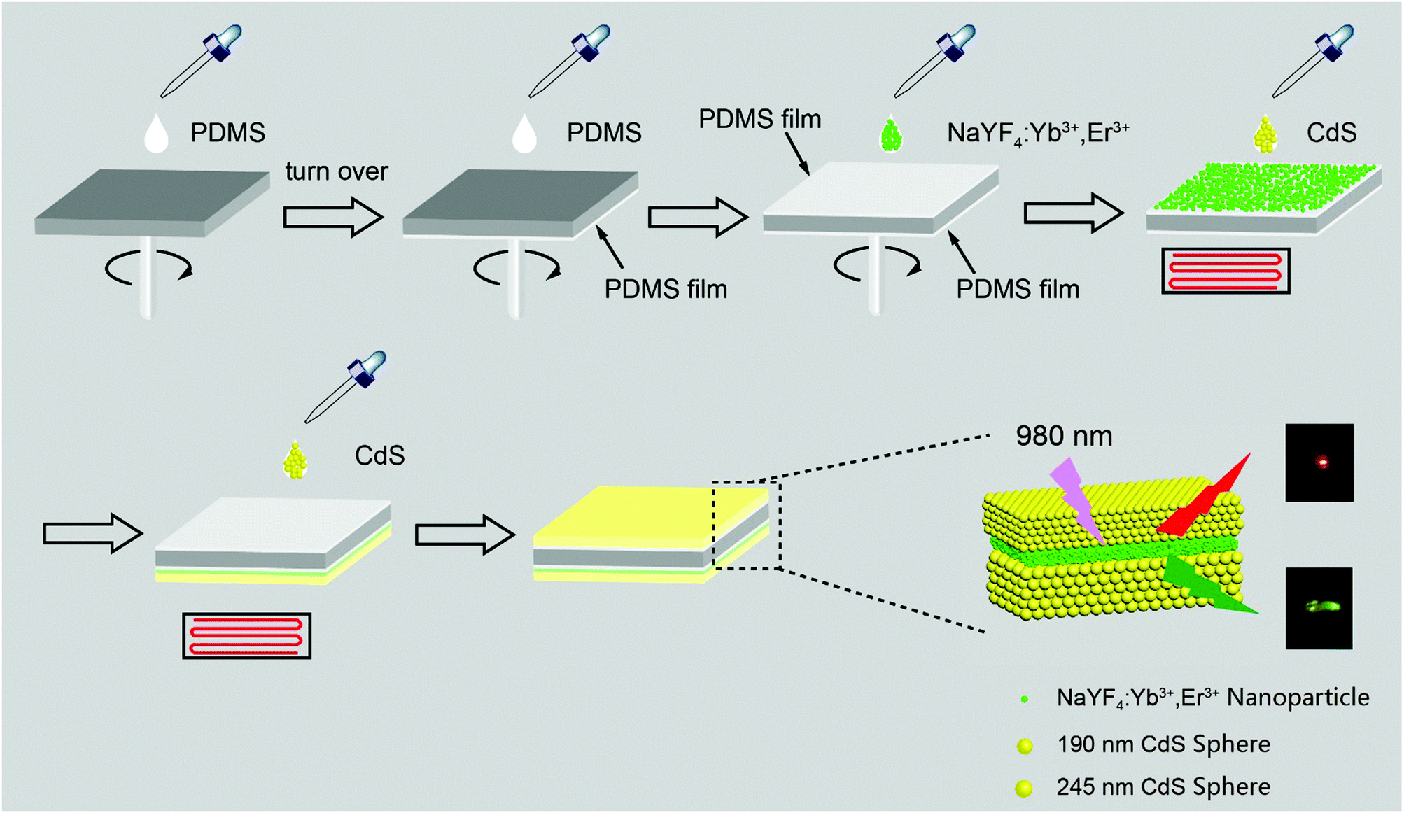 | ||
| Scheme 1 Fabrication process of the sandwich structure of PC/UCNPs/PC. | ||
Results and discussion
To validate our design, we first fabricated a two layer structure (denoted as C-2), which comprises a NaYF4:Yb3+/Er3+ nanocrystal layer on the bottom and a CdS photonic crystal layer on the top, as illustrated in Fig. 1a. NaYF4:Yb3+/Er3+ nanoparticles with a uniform size of about 14 nm were prepared through the co-precipitation method32 and characterized as pure hexagonal phase NaYF4:Yb3+/Er3+ (PDF#16-0334). Hydrophilic UCNPs remaining unchanged in shape and size were obtained by acid treatment33 to protect PDMS films, as shown in Fig. S1 (ESI†). Monodisperse CdS spheres with different diameters were prepared by our previously reported method (Fig. S2, ESI†).34,35 As a control experiment, an amorphous layer of CdS spheres with different diameters was coated on the surface of a NaYF4:Yb3+/Er3+ nanocrystal layer, and is denoted as C-1. Due to the absence of an ordered structure, the control structure has no bandgap. It is well known that NaYF4:Yb3+/Er3+ has two major bands of upconversion luminescence, which include the transitions of 2H11/2 → 4I15/2 at 525 nm and 4S3/2 → 4I15/2 at 546 nm (green emission) and 4F9/2 → 4I15/2 at 660 nm (red emission), as shown in Fig. 1c. In order to match well with the green emission of NaYF4:Yb3+/Er3+, CdS spheres with a diameter of 190 nm were selected to build the photonic crystals with a bandgap at about 530 nm (Fig. 1c). According to theory, in the designed two layer structure, the photonic crystal will forbid the transmission of light with wavelengths that overlap with its bandgap, and thereby the light will be reflected in the opposite direction as indicated in Fig. 1b. As anticipated, after coating the photonic crystal layer, the green emission of NaYF4:Yb3+/Er3+ was indeed greatly decreased, and nearly pure red emission was observed.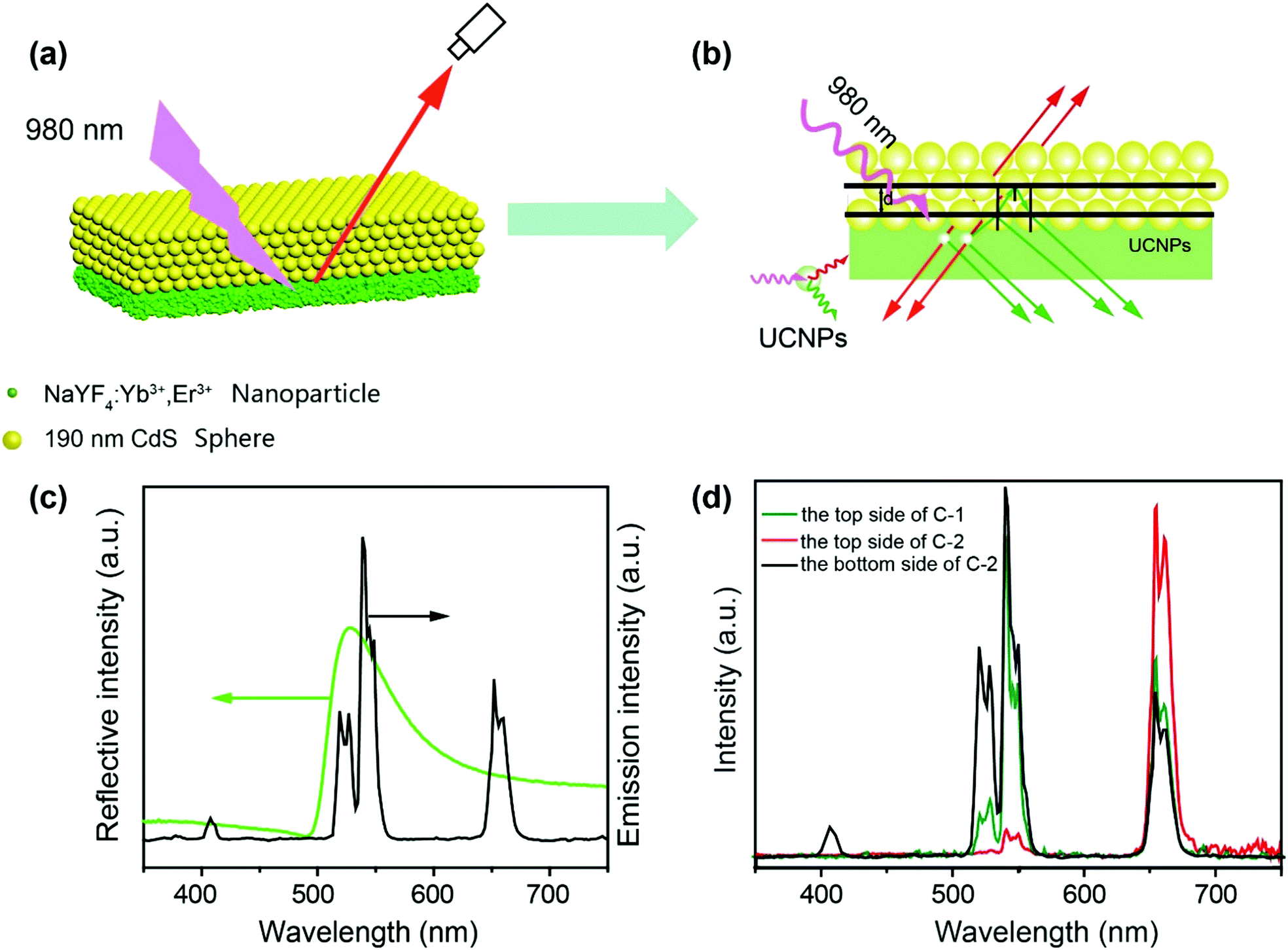 | ||
| Fig. 1 Schematic illustration of (a) the two layer structure of NaYF4:Yb3+/Er3+ and CdS photonic crystal and (b) the emitted-light propagation routes of UCNPs in the two layer structure; (c) the upconversion spectrum of NaYF4:Yb3+/Er3+ and the reflection spectrum of photonic crystals synthesized using 190 nm CdS nanoparticles as building blocks (measured at 45°); (d) the upconversion spectra of NaYF4:Yb3+/Er3+ in C-1 and C-2. | ||
To verify that the filter effect of the CdS photonic crystals originated from the bandgap, not from the absorption of light by CdS, the absorption spectra of CdS were also measured (Fig. S3, ESI†). It can be clearly seen that the absorption of CdS has no overlap with the emission of NaYF4:Yb3+/Er3+, confirming that the pure red emission is caused by the photonic bandgap rather than the intrinsic absorption of the CdS spheres. In striking contrast, when the upconversion emission was detected from the bottom side of the structure, the green emission was greatly enhanced due to the near field effect of the photonic crystals15 (Fig. 1d). By comparison, the green and red upconversion emissions of NaYF4:Yb3+/Er3+ under an amorphous CdS layer have little change due to the absence of a bandgap. Fig. S4 (ESI†) clearly indicates the basic properties of the stop bands of the different layers of CdS. These results proved that coating a layer of photonic crystals on the surface of UCNPs can indeed filter light of a frequency overlapping with the stop band to prevent its emission from the top side and enhance its emission from the bottom side.
In a further experiment, as illustrated in Scheme 1, we designed a sandwich structure (denoted as C-3). In this structure, one photonic crystal was designed to have a bandgap at about 530 nm, matching with the green emission of NaYF4:Yb3+/Er3+, and the other photonic crystal was designed to have a bandgap at about 660 nm, matching with the 4F9/2 → 4I15/2 transition (centered at 660 nm, red emission) of NaYF4:Yb3+/Er3+. First of all, a glass slide was coated by PDMS film on both sides, to guarantee the strong adhesion of UCNPs or photonic crystals on the substrate. Then a layer of UCNPs was spin-coated on the top side of the substrate. Based on Bragg's law, a photonic crystal with a bandgap of 530 nm was fabricated by the self-assembly of 190 nm CdS spheres on the surface of the UCNPs layer. Finally, CdS spheres with a diameter of 245 nm were self-assembled on the bottom side of the substrate. As displayed in Fig. 2d and e, both the photonic crystals have highly ordered structures, which will lead to a bandgap as shown in the reflection spectra in Fig. 2a. When the sandwich structure was irradiated by a 980 nm laser, the red and green emissions of the UCNPs sandwiched in the two photonic crystals were propagated in different directions due to their overlapping with the two bandgaps (Fig. 2c). The upconversion emission spectrum in Fig. 2f indicates that the green emission of the UCNPs was almost completely filtered by the photonic crystal with a bandgap of 530 nm and pure red emission was observed from the top side of the structure. On the other hand, the spectrum in Fig. 2g unveils that the red emission of the UCNPs was almost completely filtered by the photonic crystal with a bandgap of 660 nm and pure green emission was observed from the bottom side of the structure. That is to say, the green and red emissions of NaYF4:Yb3+/Er3+ are successfully separated by the sandwich structure.
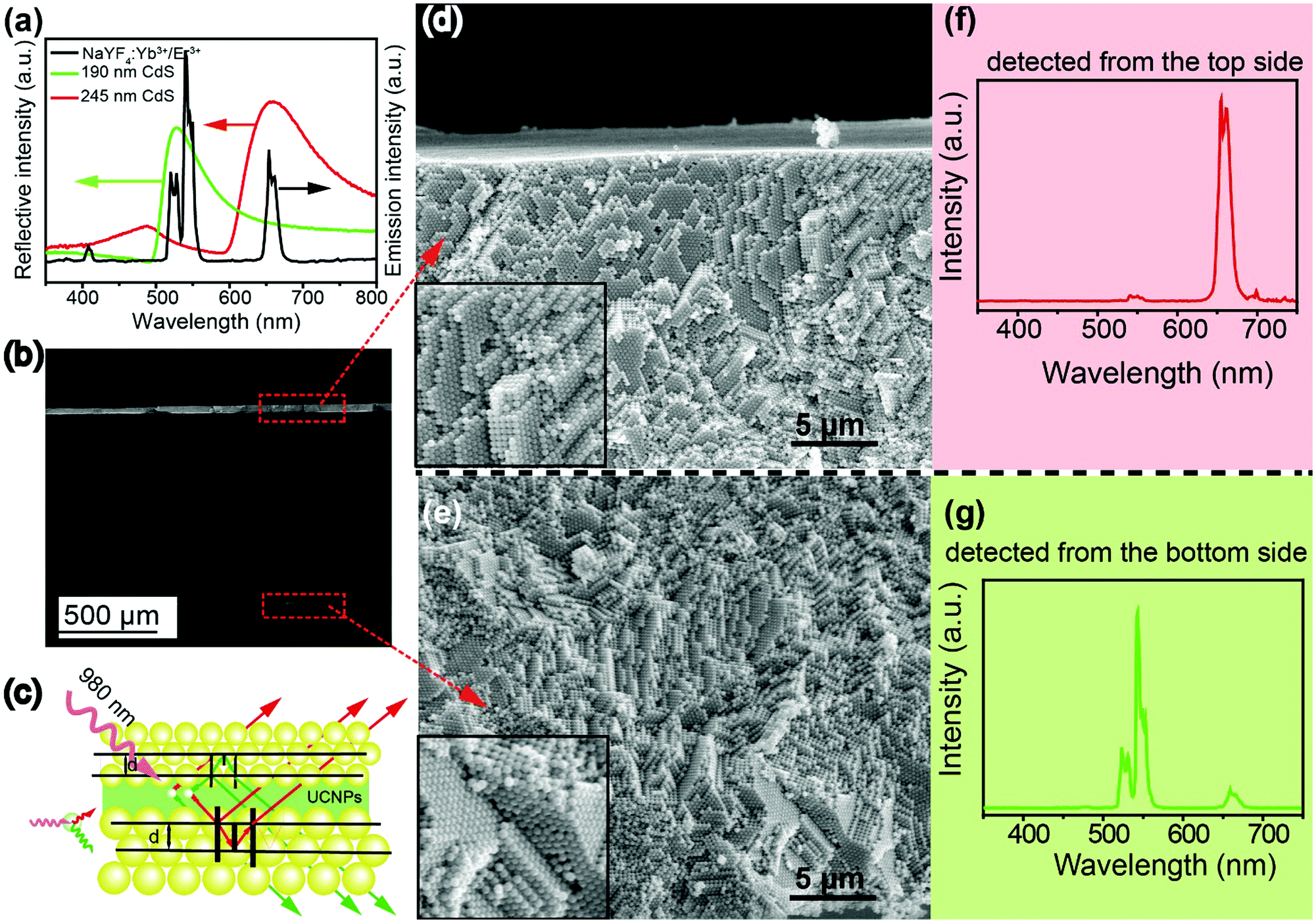 | ||
| Fig. 2 (a) The upconversion spectrum of NaYF4:Yb3+/Er3+ and the reflection spectrum of photonic crystals using 190 nm CdS and 245 nm CdS as building blocks, respectively (measured at 45°); (b) SEM images of the sandwich structure; (c) schematic illustration of the emitted-light propagation routes of UCNPs in the sandwich structure; (d) SEM images of top photonic crystal with bandgap of 530 nm; (e) SEM images of bottom photonic crystal with bandgap of 660 nm; the upconversion spectrum measured from the top side (f) and bottom side (g). | ||
To better understand the mechanism of the manipulation of the emission of UCNPs by the photonic crystals, we chose the amorphous layer of CdS and the sandwich structure as examples to clarify the effect of the photonic bandgap on the luminescence of the UCNPs. According to Fermi's golden rule,36 the radiative decay is linearly related to the DOS (density of optical states), and the existence of a bandgap in photonic crystals can redistribute the DOS. Importantly, the fluorescence lifetimes of green emission (Fig. 3a) and red emission (Fig. 3b) of NaYF4:Yb3+,Er3+ are dramatically decreased on the bottom and top sides, respectively, of the sandwich structure compared with the amorphous layer of CdS, while the emission intensities of red and green are increased on the top and bottom sides, respectively, which is very consistent with the theory. Subsequently, the dependence of Er3+ emission in the sandwich structure on excitation power was analysed (Fig. 3c and d) and the emissions at ∼544 nm and 654 nm of the UCNPs at different sides of the sandwich structure were both found to follow two-photon processes, which demonstrated that the bandgaps of the photonic crystals have no effect on the process of optical upconversion.
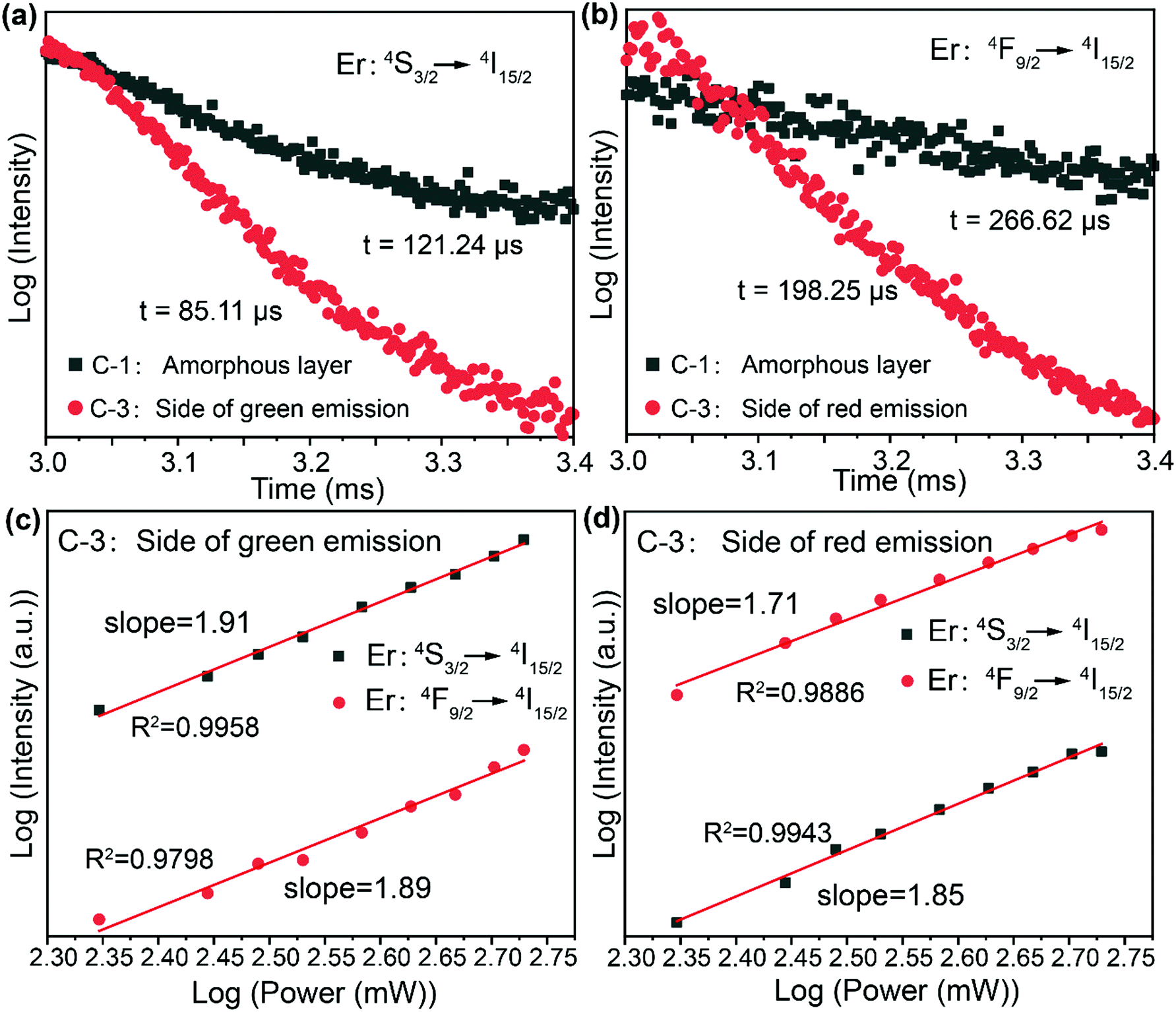 | ||
| Fig. 3 Luminescence decay curves of (a) the green emission of Er3+ ions in amorphous layer of CdS composite film C1 and in sandwich structure composite PC films C (detected from the green emission side), (b) the red emission of Er3+ ions in amorphous layer of CdS composite film C1 and in sandwich structure composite PC film C3 (detected from the red emission side), (c and d) the log–log variation curves of green and red upconversion luminescence intensity as a function of laser power for sandwich structure at different sides. | ||
To further prove the effectiveness of the photonic crystals in enhancing the emission intensity of the UCNPs, the red emissions of NaYF4:Yb3+/Er3+ in C-2 and C-3 are compared in Fig. 4a. It is obvious that the existence of photonic crystals with a bandgap at 660 nm on the bottom of C-2 enhanced the red emission of NaYF4:Yb3+/Er3+ from the top side, which verifies the near field enhancing effect of the photonic crystals. This prevents the red emission from being transmitted to the bottom side and enhances its emission from the top side. Thus, the sandwich structure realized the separating and enhancing of the red and green emission of the UCNPs simultaneously. Furthermore, the ratio of green to red (RGR) in C-3 is further reduced, that is to say the red emission detected from the top side is purer than that in C-2 (Fig. 4b).
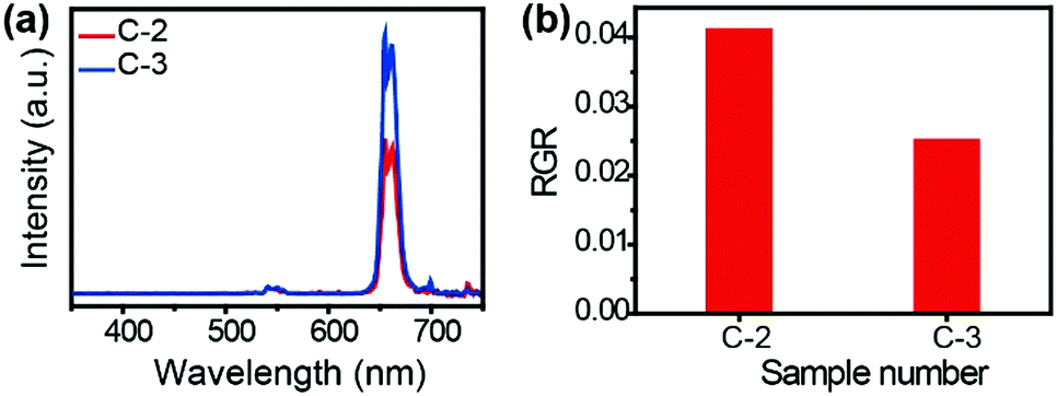 | ||
| Fig. 4 (a) The upconversion emission spectra of NaYF4:Yb3+/Er3+ in C-2 and C-3; (b) RGR of NaYF4:Yb3+/Er3+ in C-2 and C-3. | ||
For comparison, a highly ordered photonic crystal with a bandgap at 540 nm was also fabricated with 270 nm PS (polystyrene) spheres (denoted as C-4), which has a lower refractive index (1.59) than CdS (2.5).36 The reflection spectrum in Fig. 5a confirmed the existence of a bandgap at 538 nm, which is overlapped with the green emission of the UCNPs. However, in striking contrast, coating a layer of this photonic crystal on the surface of the UCNPs layer cannot filter the green light to prevent its emission from the top side (Fig. 5b), in spite of the existence of the bandgap. This phenomenon may be due to the lower refractive index of PS than that of CdS. This result indicates that photonic crystals made up of building blocks with higher refractive index have a stronger ability to manipulate light propagation.
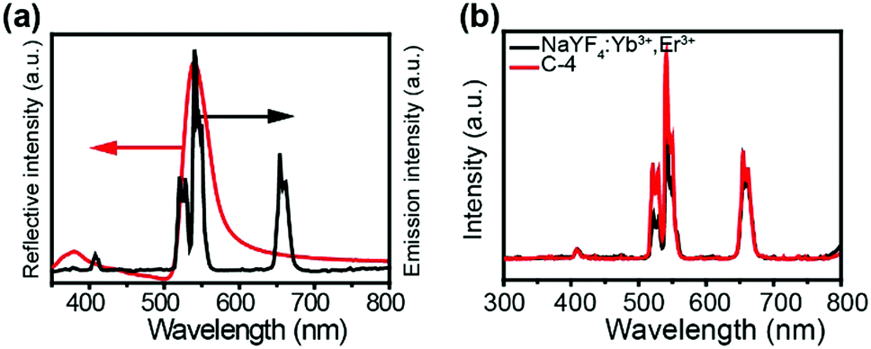 | ||
| Fig. 5 (a) Reflection spectrum (measured at 45°) of photonic crystals using 270 nm PS spheres as building blocks and upconversion emission spectrum of UCNPs; (b) upconversion emission spectrum of UCNPs combined with PS photonic crystal and with amorphous PS film. | ||
Aside from controlling the propagation of the emission light from the UCNPs, a photonic crystal was also designed with a bandgap to manipulate the excitation light. CdS spheres with a diameter of 365 nm were synthesized to fabricate this photonic crystal. As shown in Fig. 6c, the photonic crystal has a bandgap at about 980 nm, which matches well with the 980 nm laser used to excite the UCNPs. We designed a two layer structure (denoted as C-5) as displayed in Fig. 6a, in which a UCNPs layer was spin-coated on a layer of the photonic crystal made up of 365 nm CdS spheres. According to theory, when the 980 nm laser irradiates the structure, the light will be reflected back to the layer of UCNPs due to the existence of the bandgap, thereby enhancing the interaction of the 980 nm laser with the UCNPs (as illustrated in Fig. 6b). As a control experiment, the UCNPs were also spin-coated on the surface of an amorphous layer of CdS spheres (denoted as C-6). Impressively, the upconversion luminescence spectra (Fig. 6d) indicate that both the green and red emissions are dramatically enhanced in C-5 compared with that in C-6. This suggests that the interaction of the bandgap of photonic crystals with the excitation light of UCNPs indeed can increase the emission intensity greatly.
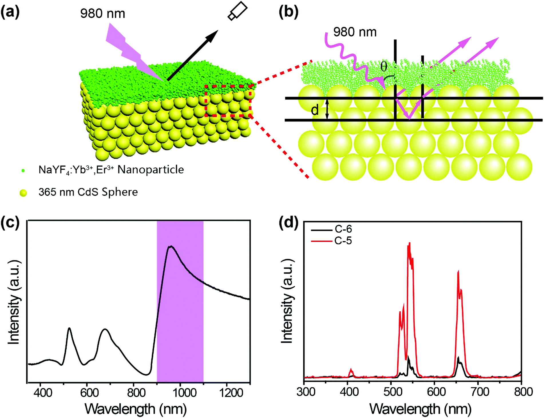 | ||
| Fig. 6 (a) Schematic illustration of a two layer structure composed of a photonic crystal (365 nm CdS) layer on the bottom and a UCNPs layer on the top; (b) schematic illustration of the propagation of 980 nm laser light in the structure; (c) reflection spectrum of the photonic crystal made up of 365 nm CdS spheres; (d) upconversion luminescence spectra of UCNPs layer on amorphous CdS film (C-6) and C-5. | ||
Experimental
Materials
Thiourea (TU), sodium hydroxide, ammonium fluoride, oleic acid (OA, 90%), methanol and styrene were purchased from Sinopharm Chemical Reagents. Cadmium(II) nitrate tetrahydrate, diethylene glycol and potassium peroxydisulfate were purchased from Tianjin GuangFu Fine Chemical Research Institute. Sodium dodecyl sulfate (SDS) was purchased from Tianjin Damao Chemical Reagents. Poly(vinylpyrrolidone) (PVP; MW = 40![[thin space (1/6-em)]](https://www.rsc.org/images/entities/char_2009.gif) 000) was purchased from Sigma-Aldrich. Yttrium acetate, ytterbium acetate and erbium acetate were purchased from Thermo Fisher Scientific. 1-Octadecene (1-ODE, 90%) was purchased from Aladdin Industrial Corporation.
000) was purchased from Sigma-Aldrich. Yttrium acetate, ytterbium acetate and erbium acetate were purchased from Thermo Fisher Scientific. 1-Octadecene (1-ODE, 90%) was purchased from Aladdin Industrial Corporation.
Synthesis of monodisperse CdS spheres
The monodisperse CdS spheres with various sizes were prepared according to our previous work. The molar ratio of Cd(NO3)2·4H2O and TU precursor was kept at 1:1 in the preparation process. For obtaining 190 nm, 245 nm and 365 nm CdS spheres, the amount of Cd(NO3)2·4H2O powder added was 10 mmol, 15 mmol and 18 mmol, respectively. A certain amount of Cd(NO3)2·4H2O and TU powder with an equal molar ratio and 4 g of PVP were dissolved in 150 mL of diethylene glycol. When all the powder was dissolved completely with vigorous stirring, the solution was transferred into a three-necked flask, and slowly heated to 165 °C for 5 h under vigorous magnetic stirring, and then cooled to room temperature with stirring. The product was washed with deionized (DI) water and ethanol three times and collected by centrifugation. Finally, the product was dried to measure the weight.
Synthesis of NaYF4:Yb3+/Er3+ and surface modification
Stock solution of lanthanide complexes (0.2 M) was prepared by dissolving the above-mentioned lanthanide acetates in DI water with an ultrasonic cleaning bath. 3 mL of OA and 7 mL of 1-ODE were first added into a 50 mL flask, then 1.6 mL of Y(CH3COO)3, 0.36 mL of Yb(CH3COO)3 and 0.04 mL of Er(CH3COO)3 were added to form a mixture. The mixture was heated at 150 °C for 40 min with stirring and then cooled down to room temperature naturally. At the same time, 2 mL of 0.5 M NaOH (methanol solution) and 3.6 mL of 0.4 M NH4F (methanol solution) were mixed in a 10 mL centrifuge tube. Then, the mixture was added into the reaction flask within 10 seconds, then heated to 50 °C and maintained for 30 min. Subsequently, the solution was heated up to 100 °C under vacuum to remove the water and oxygen left in the mixture. In an inert atmosphere, the solution was heated up to 285 °C and kept for 1.5 h. Finally, it was cooled down to room temperature slowly with stirring. NaYF4:Yb3+/Er3+ nanoparticles were collected by adding 3 mL of ethanol and centrifuging at 6000 rpm for 7 min. The UCNPs were washed three times and dispersed in 5 mL of cyclohexane. The UCNP dispersion was added into the same volume of 2 M HCl solution with an ultrasonic bath, then the ligand-free UCNPs were collected by centrifugation at 10000 rpm for 20 min. The complete removal of OA was achieved by washing three times. The products were re-dispersed in 5 mL of DI water.
Synthesis of 270 nm PS spheres
135 mL of DI water, 0.05 g of SDS and 15 g of styrene were added into a 250 mL flask. The mixture was heated to 85 °C in oil bath under N2 protection for 30 min. Then 0.15 g of potassium peroxydisulfate was added into the reaction flask. The polymerization was completed after 5 h, and the solution was cooled naturally to room temperature and used without further purification.Preparation of substrates
A 10:1 (v/v) mixture of the PDMS pre-polymer and the curing agent was deposited dropwise onto both sides of glass slides sequentially with a spin coater (Laurell WS-650SZ-6NPP/LITE) at 6000 rpm for 40 s. Then the substrates were cured at 80 °C for 2 h.
Preparation of nanocomposite films
A thin film of UCNPs was deposited on one side of the prepared substrate with a spin coater at low revolution. Then, 150 μL CdS aqueous dispersion (10 wt%) was added on the sides of the substrate, which was placed on a heating plate set at 80 °C. A film was obtained through solvent evaporation. After that, aqueous dispersions (10 wt%) of CdS particles with different diameters were dropped on the other side of the film, and then the film was put on a heating plate at 80 °C to fabricate a nanocomposite film.Characterization
The morphologies of the prepared samples and the photonic crystals were obtained by using a Nova Nanosem 450 field emission scanning electron microscope (FE-SEM). Digital photographs of the patterns were obtained with a digital camera (Nikon D7000). The reflection spectra of the photonic crystal films were measured using a Hitachi U-4100 spectrophotometer in specular reflection mode. TEM images of the UCNPs were obtained with a Tecnai G220 S-Twin at 200 kV. The prepared samples were characterized by powder X-ray diffraction (XRD) on a Rigaku D/MAX-2400 diffractometer with Cu-Kα radiation. Upconversion luminescence spectra and decay curves were obtained with an Edinburgh FS5 fluorescence spectrometer under the excitation of an external 0–2 W adjustable 980 nm CW laser.Conclusions
In conclusion, a sandwich structure comprising a NaYF4:Yb3+/Er3+ UCNPs layer between two layers of photonic crystals with bandgaps at 660 nm and 530 nm was fabricated and demonstrated to effectively separate and enhance the red and green emissions of NaYF4:Yb3+/Er3+ UCNPs. In this structure, each layer of photonic crystal acts as a nanofilter to inhibit one emission band from propagating in one direction and at the same time to enhance the emission intensity emitted in the other direction. As a result, pure and enhanced red or green emission can be observed from the top side or bottom side of the structure, respectively. Furthermore, a photonic crystal with a bandgap overlapped with the 980 nm excitation laser on the bottom of the UCNPs layer can also dramatically enhance the emission intensity of the UCNPs due to the increased interaction of the 980 nm laser and the UCNPs. Our results provide a new promising pathway for realizing strong single band emission of UCNPs by separating and enhancing the different emissions using photonic crystals.Conflicts of interest
There are no conflicts to declare.Acknowledgements
This work was supported by the National Natural Science Foundation of China (21476040, 21276040, 21536002) and the Program for Changjiang Scholars and Innovative Research Team in the University (IRT0711), Fund for innovative research groups of the National Natural Science Fund Committee of Science (21421005) and the Fundamental Research Funds for the Central Universities (DUT16TD25, DUT2016TB12).Notes and references
- X. Liu, C.-H. Yan and J. A. Capobianco, Chem. Soc. Rev., 2015, 44, 1299–1301 RSC.
- F. Wang and X. Liu, Chem. Soc. Rev., 2009, 38, 976–989 RSC.
- W. Juan and D. Renren, Chem. – Asian J., 2018, 13, 614–625 CrossRef PubMed.
- P. W. Metz, D. T. Marzahl, A. Majid, C. Kränkel and G. Huber, Laser Photonics Rev., 2016, 10, 335–344 CrossRef.
- Z. Yin, H. Li, W. Xu, S. Cui, D. Zhou, X. Chen, Y. Zhu, G. Qin and H. Song, Adv. Mater., 2016, 28, 2518–2525 CrossRef PubMed.
- C. Zhang, L. Yang, J. Zhao, B. Liu, M. Y. Han and Z. Zhang, Angew. Chem., Int. Ed., 2015, 54, 11531–11535 CrossRef PubMed.
- R. Deng, F. Qin, R. Chen, W. Huang, M. Hong and X. Liu, Nat. Nanotechnol., 2015, 10, 237 CrossRef PubMed.
- X. Li, Z. Guo, T. Zhao, Y. Lu, L. Zhou, D. Zhao and F. Zhang, Angew. Chem., Int. Ed., 2016, 55, 2464–2469 CrossRef PubMed.
- M. You, J. Zhong, Y. Hong, Z. Duan, M. Lin and F. Xu, Nanoscale, 2015, 7, 4423–4431 RSC.
- M. Li, W. Yao, J. Liu, Q. Tian, L. Liu, J. Ding, Q. Xue, Q. Lu and W. Wu, J. Mater. Chem. C, 2017, 5, 6512–6520 RSC.
- P. Kumar, K. Nagpal and B. K. Gupta, ACS Appl. Mater. Interfaces, 2017, 9, 14301–14308 CrossRef PubMed.
- S. Li, L. Xu, W. Ma, X. Wu, M. Sun, H. Kuang, L. Wang, N. A. Kotov and C. Xu, J. Am. Chem. Soc., 2016, 138, 306–312 CrossRef PubMed.
- Y. Lu, J. Zhao, R. Zhang, Y. Liu, D. Liu, E. M. Goldys, X. Yang, P. Xi, A. Sunna, J. Lu, Y. Shi, R. C. Leif, Y. Huo, J. Shen, J. A. Piper, J. P. Robinson and D. Jin, Nat. Photonics, 2013, 8, 32 CrossRef.
- S. Noda, M. Fujita and T. Asano, Nat. Photonics, 2007, 1, 449 CrossRef.
- Z. Yin, Y. Zhu, W. Xu, J. Wang, S. Xu, B. Dong, L. Xu, S. Zhang and H. Song, Chem. Commun., 2013, 49, 3781–3783 RSC.
- B. Ding, C. Hrelescu, N. Arnold, G. Isic and T. A. Klar, Nano Lett., 2013, 13, 378–386 CrossRef PubMed.
- J. Liao, Z. Yang, J. Sun, S. Lai, B. Shao, J. Li, J. Qiu, Z. Song and Y. Yang, Sci. Rep., 2015, 5, 7636 CrossRef PubMed.
- J. Liao, Z. Yang, H. Wu, D. Yan, J. Qiu, Z. Song, Y. Yang, D. Zhou and Z. Yin, J. Mater. Chem. C, 2013, 1, 6541–6546 RSC.
- W. Xu, Y. Zhu, X. Chen, J. Wang, L. Tao, S. Xu, T. Liu and H. Song, Nano Res., 2013, 6, 795–807 CrossRef.
- J. Liao, Z. Yang, S. Lai, B. Shao, J. Li, J. Qiu, Z. Song and Y. Yang, J. Mater. Chem. C, 2014, 118, 17992–17999 Search PubMed.
- L. Tao, W. Xu, Y. Zhu, L. Xu, H. Zhu, Y. Liu, S. Xu, P. Zhou and H. Song, J. Mater. Chem. C, 2014, 2, 4186–4195 RSC.
- Y. Wang, W. Xu, S. Cui, S. Xu, Z. Yin, H. Song, P. Zhou, X. Liu, L. Xu and H. Cui, Nanoscale, 2015, 7, 1363–1373 RSC.
- Y. Yang, P. Zhou, W. Xu, S. Xu, Y. Jiang, X. Chen and H. Song, J. Mater. Chem. C, 2016, 4, 659–662 RSC.
- Z.-X. Li, L.-L. Li, H.-P. Zhou, Q. Yuan, C. Chen, L.-D. Sun and C.-H. Yan, Chem. Commun., 2009, 6616–6618 RSC.
- F. Zhang, Y. Deng, Y. Shi, R. Zhang and D. Zhao, J. Mater. Chem., 2010, 20, 3895–3900 RSC.
- S. Xu, W. Xu, Y. Wang, S. Zhang, Y. Zhu, L. Tao, L. Xia, P. Zhou and H. Song, Nanoscale, 2014, 6, 5859–5870 RSC.
- Z. Yang, K. Zhu, Z. Song, D. Zhou, Z. Yin and J. Qiu, Solid State Commun., 2011, 151, 364–367 CrossRef.
- L. Zhou, R. Wang, C. Yao, X. Li, C. Wang, X. Zhang, C. Xu, A. Zeng, D. Zhao and F. Zhang, Nat. Commun., 2015, 6, 6938 CrossRef PubMed.
- T. Gan, G. Zhanjun, Z. Liangjun, Y. Wenyan, L. Xiaoxiao, Y. Liang, J. Shan, R. Wenlu, X. Gengmei, L. Shoujian and Z. Yuliang, Adv. Mater., 2012, 24, 1226–1231 CrossRef PubMed.
- D. Chen, L. Liu, P. Huang, M. Ding, J. Zhong and Z. Ji, J. Phys. Lett., 2015, 6, 2833–2840 Search PubMed.
- D. Zhou, D. Liu, W. Xu, X. Chen, Z. Yin, X. Bai, B. Dong, L. Xu and H. Song, Chem. Mater., 2017, 29, 6799–6809 CrossRef.
- F. Wang, R. Deng and X. Liu, Nat. Protoc., 2014, 9, 1634 CrossRef PubMed.
- N. Bogdan, F. Vetrone, G. A. Ozin and J. A. Capobianco, Nano Lett., 2011, 11, 835–840 CrossRef PubMed.
- S. Wu, B. Liu, X. Su and S. Zhang, J. Phys. Lett., 2017, 8, 2835–2841 Search PubMed.
- X. Su, J. Chang, S. Wu, B. Tang and S. Zhang, Nanoscale, 2016, 8, 6155–6161 RSC.
- X. Su, X. Sun, S. Wu and S. Zhang, Nanoscale, 2017, 9, 7666–7673 RSC.
Footnotes |
| † Electronic supplementary information (ESI) available: TEM images of NaYF4:Yb3+/Er3+ and ligand free NaYF4:Yb3+/Er3+, the XRD pattern of NaYF4:Yb3+/Er3+ nanoparticles (Fig. S1). SEM images of CdS spheres with different diameters: (a) 190 nm, (b) 245 nm, (c) 365 nm; (d) SEM images of amorphous layer of CdS spheres (Fig. S2), absorption spectra of the CdS films with different diameters (Fig. S3). Reflection spectra of the photonic crystal made up of 190 nm CdS spheres and the amorphous layer of CdS (Fig. S4). See DOI: 10.1039/c8nh00136g |
| ‡ These authors contributed equally to this work. |
| This journal is © The Royal Society of Chemistry 2018 |