‘Painting’ nanostructured metals—playing with liquid metal†
Zhenbin
Wang
a,
Ying
Wang
a,
Hui
Gao
a,
Jiazheng
Niu
a,
Jie
Zhang
a,
Zhangquan
Peng
b and
Zhonghua
Zhang
 *a
*a
aKey Laboratory for Liquid–Solid Structural Evolution and Processing of Materials (Ministry of Education), School of Materials Science and Engineering, Shandong University, Jingshi Road 17923, Jinan, 250061, P. R. China. E-mail: zh_zhang@sdu.edu.cn
bState Key Laboratory of Electroanalytical Chemistry, Changchun Institute of Applied Chemistry, Chinese Academy of Sciences, Changchun, Jilin 130022, P. R. China
First published on 3rd April 2018
Abstract
Materials scientists always dream to ‘paint’ nanostructured metal on a metallic foil, just as artists paint a painting on a canvas. Herein, we have, for the first time, realized this dream using liquid gallium (Ga) as the paint. Through a liquid Ga stimulated painting–alloying–dealloying strategy, seven kinds of nanostructured metallic films including Au, Ag, Pd, Pt, Cu, Co, and Ni were generally fabricated and supported on the corresponding metallic foils. Owing to the painting-like operation, nanostructured films with complicated patterns and large sizes (up to meters) were successfully produced without any shape/size limitations. The nanostructured metallic films possess advantages like their unique nanoporous structures, self-supporting nature, good continuity, flexibility and high specific surface areas, and could serve as robust electrodes in devices like batteries, fuel cells, water splitting electrolyzers, etc. Moreover, the proposed strategy shows great potential in the fabrication of other self-supporting, flexible, advanced nanomaterials.
Conceptual insightsHerein, we have, for the first time, proposed the concept of painting in the field of natural science, and indeed realized this idea using liquid gallium (Ga) with a low melting point (29.8 °C) and good fluidity as the paint. We further develop a liquid Ga-induced painting–alloying (annealing)–dealloying strategy, through which metallic nanostructures can be ‘painted’ onto metallic foils. Of great importance is that the painting strategy is general and up to seven kinds of nanostructures can be painted onto the corresponding metallic foils (Au, Ag, Pd, Pt, Cu, Co and Ni). Moreover, just like painting, nanostructured metallic films with complicated patterns could be formed without any shape and size limitations. The nanostructured metallic films owing to their unique nanoporous structures, self-supporting nature, good continuity, flexibility and high specific surface areas could serve as robust electrodes in devices like batteries, fuel cells, water splitting electrolyzers, and so forth. Through further chemical/electrochemical treatments, the foil-supported nanostructured metallic films could be transformed into oxides, hydroxides, sulfides, or layered double hydroxides with enhanced functions and performances. |
Introduction
Nanostructured metallic materials have been receiving great attention due to their combination of properties of metals with those of nanostructures. Control over the shapes, sizes and compositions of nanostructured metals plays a significant role in tuning their properties and applications. Diverse shapes of nanostructured metals have been synthesized, such as tetrahexahedron shaped Pt nanocrystals,1 one-dimensional Pd molecular wires,2 ultrathin hexagonal Pd nanosheets,3 jagged Pt nanowires,4etc. Alloying and nanocomposite architecture allow further modulation of both the morphologies and compositions of nanostructured metallic materials,5–10 for example, Pt3Ni nanoframes,11 transition metal–doped Pt3Ni octahedra,12 Pt-based nanocages,13 biaxially strained PtPb/Pt core/shell nanoplates,14 and so forth. In addition, numerous metallic nanocatalysts have been reported, like Pt-,15–18 Au-,19 Pd-,20 Cu-21 and Au–Pd-based22 catalysts. Nanostructured metallic materials normally show structure-, shape- and composition-dependent mechanical,23 physical,24–27 catalytic,28,29 and electrocatalytic11 properties and phenomena.30–33 Nanoporous (np) Au, prepared by the dealloying of AgAu alloys, could catalyze the selective oxidative coupling of methanol to methyl formate with high selectivities and turnover frequencies under mild conditions.29 Both the interior and exterior Pt-skin-decorated surfaces of Pt3Ni nanoframes could provide numerous active sites, highly catalyzing the oxygen reduction reaction (ORR).11Owing to their unique microstructures and related properties, nanostructured metallic materials show great potential in applications like sensors, actuators,34,35 energy conversion and storage,36,37etc. For example, hybrid structures made of np-Au and nanocrystalline MnO2 could enhance electrical conductivity for high-performance electrochemical supercapacitors.36 Peng et al.37 reported that a high-rate Li–O2 cell composed of a dimethyl sulfoxide electrolyte and a np-Au electrode can sustain reversible cycling with a retention capacity of 95% after 100 cycles and have >99% purity of Li2O2 formation at the cathode. Different kinds of synthetic routes have been proposed to fabricate nanostructured metallic materials, such as surfactant-assisted decomposition of organometallic precursors,38 reduction of metal salts,7,39 galvanic replacement,39 electrochemical treatment using square-wave potential pulses,1 CO-confined solvothermal synthesis,3 self-assembly,40 selective dissolution (or dealloying),4,13,41etc. A solution-based approach is an effective technique to fabricate crystallographic facet-directed nanocatalysts, and is aided by careful selection of the metal precursor, capping ligand, reducing agent, and solvent.17,42 However, it is still a great challenge to generally synthesize continuous, flexible, self-supporting nanostructured metal films.
Painting is essential for artists, and scientists also dream to synthesize nanostructured materials like painting mastered by artists. Here we show that painting could indeed be utilized to fabricate continuous, flexible, self-supporting nanostructured metal films, with liquid gallium (Ga) as the paint. Ga has a low melting point of 29.8 °C and has received special attention in phase transition,43 the synthesis of GaN nanowires/nanotubes,44,45 temperature sensors,46 and liquid motors.47 Through liquid Ga induced alloying/dealloying, we generally synthesized nanostructured metals supported on metallic foils including Au, Ag, Pd, Pt, Cu, Co and Ni. Moreover, these metallic nanostructures could form on foils without any shape and size limitations just like painting, and samples with complicated patterns and sizes up to meters could be obtained. More importantly, these self-supporting nanostructured metals could be directly used as functional electrodes and be well integrated into devices like batteries, supercapacitors, fuel cells, water splitting electrolyzers, and so forth.
Methods
Sample fabrication
We used liquid Ga (purity, 99.99 wt%) as the ‘paint’ for all painting. Before painting, the commercial Au, Ag, Pd, Pt, Cu, Co and Ni foils (purity, 99.99 wt%) were cleaned with acetone, deionized water and alcohol. The Ga ingot was melted at 40 °C and liquid Ga was kept at this temperature for use. The metallic foils (designated as M) were put onto a heating plate which was set at 40 °C during the painting process. Using a paintbrush, liquid Ga was painted onto the surfaces of the metallic foils to form films (Movie S1, ESI†). In order to realize the alloying of liquid Ga with the metallic substrate, the painted metallic foils were annealed at different temperatures for different durations. The painted Au, Ag, Cu and Ni foils were annealed at 100 °C for 5 hours, and the painted Pd, Pt and Co foils were annealed at 150 °C for 10 hours to induce the formation of GaxMy intermetallic phases. Subsequently, the annealed metallic foils were dealloyed at room temperature until no obvious bubbles emerged. A 2.0 M HNO3 aqueous solution was used for dealloying of the annealed Au, Ag, Pd and Pt foils. The dealloying of the annealed Cu foils was performed in a 0.2 M HNO3 aqueous solution. In addition, the annealed Ni and Co foils were dealloyed in a 0.1 M and 5.0 M NaOH aqueous solution, respectively. The as-dealloyed samples were washed with ultra-pure water and alcohol before being dried in a vacuum.Microstructural characterization
X-ray diffraction (XRD) measurements of all samples were performed on an XD-3 diffractometer (Beijing Purkinje General Instrument Co., Ltd, China) with Cu Kα radiation. The microstructures and chemical compositions of the as-dealloyed samples were characterized using a scanning electron microscope (SEM, ZEISS SIGMA300), equipped with an energy dispersive X-ray (EDX) analyzer.Electrochemical measurements
All electrochemical measurements were performed on a CHI760E potentiostat in a standard three-electrode cell, with an Ag/AgCl electrode used as the reference electrode, a bright Pt plate used as the counter electrode, and the as-prepared np-Au, Pt and Pd films (area: 1 × 1 cm2) used as the working electrodes. The working electrodes were subjected to cyclic voltammetry (CV) scans at 50 mV s−1 in a N2-saturated 0.5 M H2SO4 aqueous solution. The amount of charge consumed (390 μC cm−2) during the reduction of the Au surface oxide monolayer was used to calculate the electrochemically active area (EAA) of the np-Au film.48 The EAA value of the np-Pd film was evaluated from the reduction charge of Pd(OH)2 and the reported charge density was 430 μC cm−2.49 The EAA of the np-Pt film was determined from hydrogen adsorption/desorption charges (210 μC cm−2) of CVs.50 In addition, the EAA of the np-Au film was calculated after different ultrasonic times (1, 5, 10 and 20 min) to measure the bonding strength of the nanoporous Au layer with the support. Moreover, the ORR activity of the np-Ag film (area: 1 × 1 cm2) was measured in an O2-saturated 0.1 M KOH solution without and with stirring at a scan rate of 10 mV s−1. For comparison, the catalytic performances of Ag foil and Pt foil (area: 1 × 1 cm2) towards the ORR were also evaluated under identical experimental conditions without stirring.Results and discussion
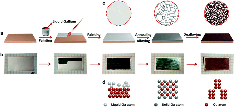
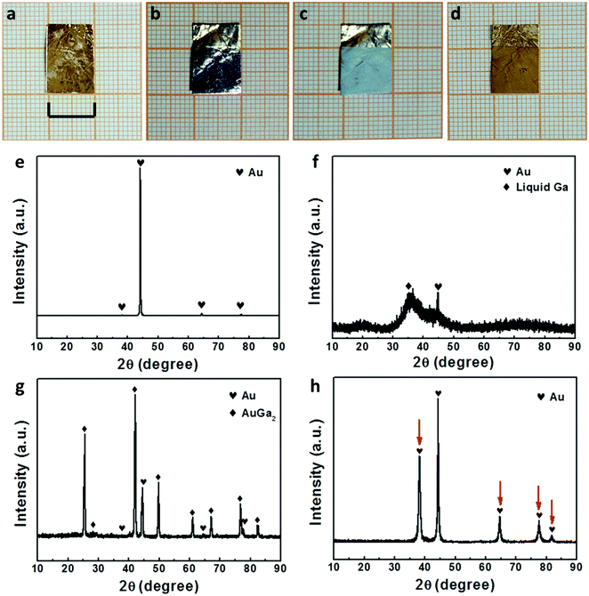
Liquid Ga has good fluidity at room temperature (above 30 °C) and could be well handled like the paint (Fig. S1, ESI†). For the first time, herein, we have proposed a liquid Ga induced painting–alloying–dealloying strategy for the general fabrication of nanostructured metallic films supported on metal foils, as schematically illustrated in Fig. 1. Using a paintbrush, liquid Ga could be facilely painted onto any metal foil (Movie S1, ESI† here Au, Ag, Pd, Pt, Cu, Co, and Ni were used). During subsequent annealing, liquid Ga reacted with the metal substrate to form a solid GaxMy intermetallic phase through a liquid–solid reaction. Finally, the GaxMy layer was dealloyed to form a nanostructured metallic film supported on the metal substrate. Fig. 1b shows the scenario of Cu, and the serial photographs clearly show the formation process of a nanostructured Cu film (area: 4 × 8 cm2) supported on a Cu foil. The nanostructured Cu film is dark red, and different from the silvery color of the CuGa2 phase and the painted liquid Ga.Taking Au as an example, we further illustrate the surface and phase evolution during the liquid Ga induced alloying–dealloying process, Fig. 2. The commercial Au foil has a golden appearance (Fig. 2a), and consists of a single face centered cubic (fcc) Au phase (PDF # 04-0784) with a (200) orientation (Fig. 2e). After being painted with liquid Ga, the covered surface of the Au foil displays a silvery color (Fig. 2b). The XRD result confirms the existence of liquid Ga on the surface of the Au foil, as indicated by a broad hump in Fig. 2f. After annealing, a unique cyan color appears on the Au foil surface (Fig. 2c) and the XRD result (Fig. 2g) verifies the formation of an AuGa2 intermetallic phase (PDF # 03-0969) owing to the alloying reaction between liquid Ga and solid Au during annealing. After further dealloying, a dark yellow color can be observed on the Au foil surface (Fig. 2d), and only the fcc Au phase can be detected in the as-dealloyed Au foil (Fig. 2h). Notably, the intensities of the (111), (220), (311) and (222) peaks of the as-dealloyed sample are significantly enhanced in comparison to those of the pristine Au foil (as highlighted by red arrows in Fig. 2h), indicating the formation of nanostructured Au due to the dealloying of AuGa2.
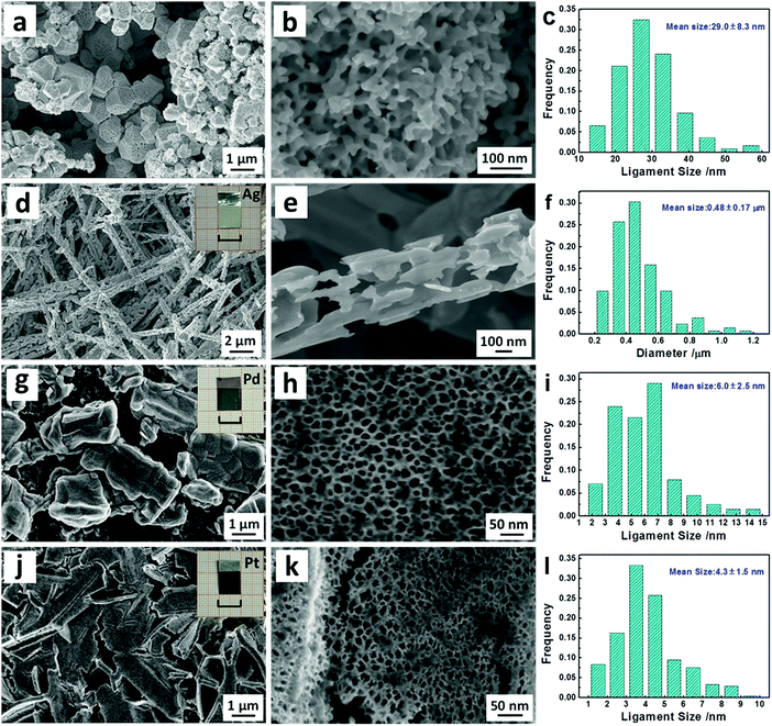
The microstructures of the obtained nanostructured metallic films (area: 1 × 1 cm2) were characterized by SEM. The nanostructured Au film is composed of micron-sized particles (around 1 μm in size) gathered together, Fig. 3a and Fig. S2a (ESI†). Interestingly, these micro-particles display a typical nanoporous structure consisting of bicontinuous ligaments and channels at higher magnifications, Fig. 3b and Fig. S2b (ESI†). The size distribution of ligaments in the np-Au film is shown in Fig. 3c and the mean ligament scale is 29.0 ± 8.3 nm. The composition of the np-Au film was determined to be 97.4 at% Au and 2.6 at% Ga using an EDX analyzer, Fig. S2c (ESI†).
Other nanostructured metallic films can be fabricated via a similar painting–alloying–dealloying procedure. As for Ag, an Ag3Ga intermetallic phase (PDF # 47-0991) was formed on an Ag foil surface after the painting–annealing treatment (Fig. S3a–e, ESI†). After further dealloying, only the fcc Ag phase (PDF # 04-0783) can be detected (Fig. S3f, ESI†) and the appearance (dark silvery) of the sample is different from that of the pristine bright Ag foil (inset of Fig. 3d). Massive micron-sized wires can be observed in the as-dealloyed Ag foil and entangle each other to form a continuous network (Fig. 3d and Fig. S4a, ESI†). Surprisingly, each Ag wire is highly nanoporous (Fig. S4b, ESI†) and one porous Ag microwire is highlighted in Fig. 3e. The diameter distribution of Ag microwires is shown in Fig. 3f and the mean value is 0.48 ± 0.17 μm. In addition, the residual Ga content is as low as 0.62 at% in these porous Ag microwires (Fig. S4c, ESI†).
It is known that nanostructured Pd and Pt are excellent catalysts, and we thus pay attention to the synthesis of nanoporous Pd/Pt supported on the Pd/Pt foil using the present strategy. Through the annealing-induced liquid–solid reaction, a PdxGay intermetallic phase occurred on the painted surface of the Pd foil (Fig. S5a–e, ESI†). After further dealloying, a new broad diffraction peak appears on the XRD pattern of the as-dealloyed Pd foil, which is superimposed on the sharp (111) reflection of fcc Pd (PDF # 46-1043), Fig. S5f–h (ESI†). The SEM observation indicates irregular particles (less than 5 μm in size) in the as-dealloyed film supported on the Pd foil (Fig. 3g and Fig. S6a, ESI†). The high-magnification SEM images clearly show an ultrafine nanoporous structure of the as-dealloyed layer (Fig. 3h and Fig. S6b, ESI†). Notably, the average ligament size is only 6.0 ± 2.5 nm, as indicated by the size distribution in Fig. 3i. The residual Ga content is close to 20.0 at% in the np-Pd film (Fig. S6c, ESI†), implying the formation of an fcc Pd(Ga) solid solution alloy. Moreover, this solid solution of ∼20.0 at% Ga in Pd causes a slight right shift of the broad peak of np-Pd in comparison to the (111) reflection of the fcc Pd phase (Fig. S5g, ESI†). Through a similar procedure, an ultrafine np-Pt film supported on the Pt foil can also be obtained (Fig. 3j–l and Fig. S7, S8, ESI†). A Ga2Pt phase (PDF # 03-1007) was formed after annealing the Pt foil covered with liquid Ga (Fig. S7e, ESI†), and the dealloying of Ga2Pt resulted in the formation of np-Pt (Fig. S7f, ESI†). The average ligament size is as small as 4.3 ± 1.5 nm (Fig. 3l) and the residual Ga content is also close to 20 at% in the np-Pt film (Fig. S8c, ESI†), which leads to the significant broadening of the (111) peak on the XRD pattern of np-Pt (Fig. S7g, ESI†). With respect to the formation and microstructure, the scenario of np-Pt is analogous to that of np-Pd. In addition, the crystal (grain) sizes of np-Pd and np-Pt were determined to be 2.6 and 4.3 nm through the Scherrer equation, respectively.
Besides noble metals (Au, Ag, Pd and Pt), the proposed strategy can also be applied for base metals like Cu, Co and Ni. After the painting–annealing treatment, a CuGa2 phase (PDF # 25-0275) was formed on the surface of the Cu foil (Fig. S9a–e, ESI†), and only the fcc Cu phase (PDF # 04-0836) was identified in the as-dealloyed sample (Fig. S9f, ESI†). As can be seen from Fig. S10a (ESI†) (back-scattered SEM image), the grain shape and size can be clearly observed in the as-annealed CuGa2 layer. The Cu![[thin space (1/6-em)]](https://www.rsc.org/images/entities/char_2009.gif) :
:![[thin space (1/6-em)]](https://www.rsc.org/images/entities/char_2009.gif) Ga atomic ratio in the as-annealed layer was determined by EDX (Fig. S10b, ESI†) to be around 1
Ga atomic ratio in the as-annealed layer was determined by EDX (Fig. S10b, ESI†) to be around 1![[thin space (1/6-em)]](https://www.rsc.org/images/entities/char_2009.gif) :
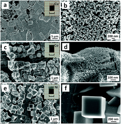
:![[thin space (1/6-em)]](https://www.rsc.org/images/entities/char_2009.gif) 2, which further indicates the presence of a CuGa2 phase. In addition, the elemental mapping spectra of Cu (Fig. S10d, ESI†) and Ga (Fig. S10e, ESI†) clearly reveal the uniform distribution of both elements in the as-annealed Cu–Ga film. A typical bicontinuous ligament-channel structure appears in the dealloyed layer of the Cu foil (Fig. 4a, b, and Fig. S11a, b, ESI†), indicating the formation of a dark red np-Cu film (inset of Fig. 4a). The ligament sizes range from 50 to 200 nm (Fig. 4b), and the residual Ga content is less than 1.0 at% in the obtained np-Cu film (Fig. S11c, ESI†). Furthermore, a grain-like characteristic can be clearly observed from the low-magnification SEM images of np-Cu (Fig. 4a and Fig. S11a, ESI†). By comparing with the back-scattered SEM image of the as-annealed Cu foil (Fig. S10a, ESI†), we assume that the grain-like morphology of np-Cu was inherited from that of CuGa2 grains in the as-annealed layer. The corresponding microstructural evolution during the painting–annealing (alloying)–dealloying process is schematically illustrated in Fig. 1c. With respect to the scenario of Co, the annealing of the painted liquid Ga layer brought about the formation of a CoGa3 phase (PDF # 15-0578) (Fig. S12a–e, ESI†), and the dealloying of CoGa3 led to the occurrence of a hexagonal Co phase (PDF # 05-0727) (Fig. S12f, ESI†). The obtained np-Co film (inset of Fig. 4c) is composed of massive micron-sized particles which are nanoporous and have a ligament size of 16.3 ± 6.7 nm (Fig. 4c, d and Fig. S13a, b, ESI†). And several at% Ga was retained in the np-Co film (Fig. S13c, ESI†). As for Ni, an NiGa4 phase (PDF # 37-1095) was formed on the annealed surface of the Ni foil (Fig. S14a–e, ESI†), and only the fcc Ni phase (PDF # 04-0850) was detected in the as-dealloyed sample (Fig. S14f, ESI†). Interestingly, submicron-sized Ni polyhedra (cubes and octahedra) are observed in the as-dealloyed layer of the Ni foil (Fig. 4e, f and Fig. S15a, b, ESI†). One Ni cube is highlighted in Fig. 4f. The Ni
2, which further indicates the presence of a CuGa2 phase. In addition, the elemental mapping spectra of Cu (Fig. S10d, ESI†) and Ga (Fig. S10e, ESI†) clearly reveal the uniform distribution of both elements in the as-annealed Cu–Ga film. A typical bicontinuous ligament-channel structure appears in the dealloyed layer of the Cu foil (Fig. 4a, b, and Fig. S11a, b, ESI†), indicating the formation of a dark red np-Cu film (inset of Fig. 4a). The ligament sizes range from 50 to 200 nm (Fig. 4b), and the residual Ga content is less than 1.0 at% in the obtained np-Cu film (Fig. S11c, ESI†). Furthermore, a grain-like characteristic can be clearly observed from the low-magnification SEM images of np-Cu (Fig. 4a and Fig. S11a, ESI†). By comparing with the back-scattered SEM image of the as-annealed Cu foil (Fig. S10a, ESI†), we assume that the grain-like morphology of np-Cu was inherited from that of CuGa2 grains in the as-annealed layer. The corresponding microstructural evolution during the painting–annealing (alloying)–dealloying process is schematically illustrated in Fig. 1c. With respect to the scenario of Co, the annealing of the painted liquid Ga layer brought about the formation of a CoGa3 phase (PDF # 15-0578) (Fig. S12a–e, ESI†), and the dealloying of CoGa3 led to the occurrence of a hexagonal Co phase (PDF # 05-0727) (Fig. S12f, ESI†). The obtained np-Co film (inset of Fig. 4c) is composed of massive micron-sized particles which are nanoporous and have a ligament size of 16.3 ± 6.7 nm (Fig. 4c, d and Fig. S13a, b, ESI†). And several at% Ga was retained in the np-Co film (Fig. S13c, ESI†). As for Ni, an NiGa4 phase (PDF # 37-1095) was formed on the annealed surface of the Ni foil (Fig. S14a–e, ESI†), and only the fcc Ni phase (PDF # 04-0850) was detected in the as-dealloyed sample (Fig. S14f, ESI†). Interestingly, submicron-sized Ni polyhedra (cubes and octahedra) are observed in the as-dealloyed layer of the Ni foil (Fig. 4e, f and Fig. S15a, b, ESI†). One Ni cube is highlighted in Fig. 4f. The Ni![[thin space (1/6-em)]](https://www.rsc.org/images/entities/char_2009.gif) :
:![[thin space (1/6-em)]](https://www.rsc.org/images/entities/char_2009.gif) Ga atomic ratio is close to 3
Ga atomic ratio is close to 3![[thin space (1/6-em)]](https://www.rsc.org/images/entities/char_2009.gif) :
:![[thin space (1/6-em)]](https://www.rsc.org/images/entities/char_2009.gif) 1 in the nanostructured Ni film (Fig. S15c, ESI†). Additionally, both the np-Co and nanostructured Ni films are black (insets of Fig. 4c and e), which are different from the bright silvery appearance of Co and Ni foils. It should be noted that a certain amount of oxygen was detected in the as-dealloyed Co/Ni samples (Fig. S13c and S15c, ESI†), due to the high activity and easy surface oxidation of nanostructured Co/Ni during the dealloying, drying and storage processes.
1 in the nanostructured Ni film (Fig. S15c, ESI†). Additionally, both the np-Co and nanostructured Ni films are black (insets of Fig. 4c and e), which are different from the bright silvery appearance of Co and Ni foils. It should be noted that a certain amount of oxygen was detected in the as-dealloyed Co/Ni samples (Fig. S13c and S15c, ESI†), due to the high activity and easy surface oxidation of nanostructured Co/Ni during the dealloying, drying and storage processes.
We thus discuss the formation mechanism of the nanostructured films supported on the metallic foils. Here Cu is taken as an example (Fig. 1d). During annealing, liquid Ga atoms with a disordered arrangement reacted with the ordered solid Cu atoms to form an intermetallic phase (CuGa2). In CuGa2, Cu and Ga atoms mix on the atomic scale, which is a prerequisite for dealloying of a precursor to form a nanoporous structure.51 It is known that the active element is selectively etched away in an appropriate corrosive solution, and the less active element diffuses along the alloy/solution interface and re-organizes into a nanoporous structure during dealloying.51–53 Due to the difference in chemical activity between Cu and Ga, the Ga in CuGa2 was preferentially dissolved and the released Cu adatoms re-organized to form a nanoporous structure through surface diffusion during dealloying in the 0.2 M HNO3 solution (Fig. 1d). A similar mechanism also applies to the formation of other nanostructured metallic films. Through the painting–annealing (alloying) treatment, Ga-containing intermetallic layers (AuGa2, Ag3Ga, PdxGay, Ga2Pt, CoGa3 and NiGa4) were formed on the surfaces of metallic foils. The further dealloying of these intermetallic layers resulted in the formation of nanostructured metallic films (np-Au, etc.), involving the selective dissolution of Ga and surface diffusion/re-organization of the inactive element (Au, etc.). Moreover, the length scale of ligaments in the nanoporous films depends on the diffusivity of the inactive element during dealloying.52 The diffusion of Pt and Pd is several orders of magnitude lower than that of Au.52,54 Therefore, the average ligament sizes (6.0 ± 2.5 nm for Pd and 4.3 ± 1.5 nm for Pt) of np-Pd and np-Pt are much smaller than that (29.0 ± 8.3 nm) of np-Au.
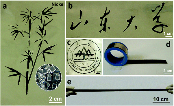
Due to the paint-like nature of liquid Ga, we can, in principle, design any pattern of nanostructured films on a metallic foil without size limitations, as an artist paints a painting on a canvas. Using a Ni foil as the ‘canvas’, here we show some examples for the design of nanostructured metallic films. It should be noted that the proposed strategy is not limited to these examples. As displayed in Fig. 5a and Fig. S16 (ESI†), we ‘painted’ a bamboo on the Ni foil through the painting–annealing–dealloying strategy. The microstructure of the bamboo is highlighted as an inset in Fig. 5a. More complicated patterns were also achieved, like Chinese characters (Fig. 5b and Fig. S17, ESI†) and the school logo (Fig. 5c and Fig. S18, ESI†) of Shandong University. More importantly, a nanostructured Ni foil with a length of up to 50 cm was facilely obtained (Fig. 5d, e and Fig. S19, S20, ESI†), indicating the controllability of the present strategy for large-scale preparation. Moreover, the nanostructured Ni foil can be easily handled, like rolling-up or evolving (Fig. 5d, e and Fig. S20, ESI†), totally depending on the flexibility of the supported foil. In addition, Fig. 1b demonstrates the fabrication of a np-Cu film with dimensions of 4 × 8 cm2 on the Cu foil.
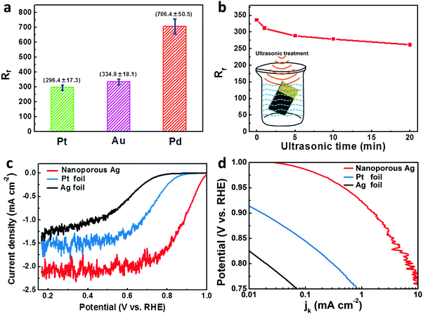
For practical applications, the EAA and the related roughness factor (Rf, the ratio of EAA to the geometric area) are crucial to electrocatalysts like Pt, Pd, etc. Through CV measurements (Fig. S21, ESI†), the EAA values of the metallic foil-supported np-Pt, np-Au and np-Pd films were determined. The corresponding roughness factors were calculated and are shown in Fig. 6a. Owing to their unique nanoporous structure, these np-Pt, np-Au and np-Pd films show ultrahigh Rf values of 296.4 ± 17.3, 334.9 ± 18.1 and 706.4 ± 50.5, respectively. Additionally, to evaluate the bonding strength of the nanoporous film with the supported foil, the np-Au film was subjected to ultrasonic treatment in ultrapure water for different times (inset of Fig. 6b). Fig. 6b shows the influence of the ultrasonic time on the roughness factor of the np-Au film, and the corresponding CV curves are displayed in Fig. S21d (ESI†). The Rf of the np-Au film slightly decreases with increasing ultrasonic time, indicative of the excellent bonding of the nanoporous layer with the support. Even after the ultrasonic treatment of 20 min, the Rf of np-Au is still 261.6, retaining ∼78% of its initial value.
Considering the unique nanostructure, high EAA, self-supporting nature, flexibility and excellent bonding, the present foil-supported nanostructured metallic films could be promising electrode materials for applications in electrocatalysis, energy storage, and so forth. Here we just show the electrocatalytic performance of the Ag foil-supported np-Ag film towards the ORR in an O2-saturated 0.1 M KOH solution (Fig. 6c and Fig. S22, ESI†). Under the same test conditions, the np-Ag film exhibits much better electrocatalytic activity towards the ORR than the bulk Ag foil. Even as benchmarked with the bulk Pt foil, the np-Ag film still shows superior ORR activity. Both the onset potential and half-wave potential of the np-Ag film are more positive than those of the bulk Ag and Pt foils. Furthermore, the limiting current of np-Ag in the diffusion-controlled region is much higher than those of bulk Ag and Pt (Fig. 6c). It should be noted that the significant fluctuations of currents in the diffusion-controlled potential region originate from the competition between O2 and the adsorbed OH (or other reaction intermediates) for the active sites, and the high coverage of OH will hinder the O2 adsorption on the reaction sites under static test conditions (the np-Ag/bulk Ag/bulk Pt electrodes were not rotated).55 Once the electrolyte was stirred, the limiting current of np-Ag was further enhanced (Fig. S22, ESI†). To achieve a better comparison of their electrocatalytic activities, the kinetic current densities (jk) of the three electrodes were calculated using the Koutecky–Levich equation and are presented as the Tafel plots in Fig. 6d. Clearly, the np-Ag film exhibits higher activity (much larger kinetic currents) than bulk Ag and Pt in the potential range of 0.75–1.0 V vs. RHE. The enhanced activity of np-Ag could be attributed to the unique nanoporous structure and associated high specific surface area. In addition, the monolithic nanoporous microwire network and the self-supporting nature could cause a geometric effect,56 which also plays a role in enhancing the ORR activity of np-Ag.
Conclusions
In summary, due to its good fluidity at room temperature, liquid Ga can be facilely painted onto the surfaces of metallic foils. Through the liquid Ga induced alloying–dealloying strategy, nanostructured metallic films (here Au, Ag, Pd, Pt, Cu, Co and Ni) can be generally fabricated and supported on the corresponding metals without any shape and size limitations. These nanostructured films could be produced into complex patterns and large sizes (up to meters), and show unique advantages like the self-supporting nature, good continuity, flexibility, high specific surface areas, and so forth. Further, the nanostructured metallic films could directly serve as robust electrodes in devices like batteries, fuel cells, water splitting electrolyzers, etc. The present strategy also shows great potential in the fabrication of other self-supporting, flexible, nanostructured metals, hydroxides, oxides, and so on.Conflicts of interest
There are no conflicts to declare.Acknowledgements
The authors gratefully acknowledge financial support from the National Natural Science Foundation of China (51671115), and the support of the Department of Science and Technology of Shandong Province for the Young Tip-top Talent Support Project, and the Young Tip-top Talent Support Project (the Organization Department of the Central Committee of the CPC).References
- N. Tian, Z.-Y. Zhou, S.-G. Sun, Y. Ding and Z. L. Wang, Science, 2007, 316, 732–735 CrossRef CAS PubMed.
- M. G. Campbell, D. C. Powers, J. Raynaud, M. J. Graham, P. Xie, E. Lee and T. Ritter, Nat. Chem., 2011, 3, 949–953 CrossRef CAS PubMed.
- X. Huang, S. Tang, X. Mu, Y. Dai, G. Chen, Z. Zhou, F. Ruan, Z. Yang and N. Zheng, Nat. Nanotechnol., 2011, 6, 28–32 CrossRef CAS PubMed.
- M. Li, Z. Zhao, T. Cheng, A. Fortunelli, C.-Y. Chen, R. Yu, Q. Zhang, L. Gu, B. V. Merinov and Z. Lin, Science, 2016, 354, 1414–1419 CrossRef CAS PubMed.
- H. Fan, K. Yang, D. M. Boye, T. Sigmon, K. J. Malloy, H. Xu, G. P. López and C. J. Brinker, Science, 2004, 304, 567–571 CrossRef CAS PubMed.
- S. H. Joo, J. Y. Park, C.-K. Tsung, Y. Yamada, P. Yang and G. A. Somorjai, Nat. Mater., 2009, 8, 126–131 CrossRef CAS PubMed.
- B. Lim, M. Jiang, P. H. Camargo, E. C. Cho, J. Tao, X. Lu, Y. Zhu and Y. Xia, Science, 2009, 324, 1302–1305 CrossRef CAS PubMed.
- K. Tedsree, T. Li, S. Jones, C. W. A. Chan, K. M. K. Yu, P. A. Bagot, E. A. Marquis, G. D. Smith and S. C. E. Tsang, Nat. Nanotechnol., 2011, 6, 302–307 CrossRef CAS PubMed.
- H.-G. Liao, L. Cui, S. Whitelam and H. Zheng, Science, 2012, 336, 1011–1014 CrossRef CAS PubMed.
- D. Wang, H. L. Xin, R. Hovden, H. Wang, Y. Yu, D. A. Muller, F. J. DiSalvo and H. D. Abruña, Nat. Mater., 2013, 12, 81–87 CrossRef CAS PubMed.
- C. Chen, Y. Kang, Z. Huo, Z. Zhu, W. Huang, H. L. Xin, J. D. Snyder, D. Li, J. A. Herron and M. Mavrikakis, Science, 2014, 343, 1339–1343 CrossRef CAS PubMed.
- X. Huang, Z. Zhao, L. Cao, Y. Chen, E. Zhu, Z. Lin, M. Li, A. Yan, A. Zettl and Y. M. Wang, Science, 2015, 348, 1230–1234 CrossRef CAS PubMed.
- L. Zhang, L. T. Roling, X. Wang, M. Vara, M. Chi, J. Liu, S.-I. Choi, J. Park, J. A. Herron and Z. Xie, Science, 2015, 349, 412–416 CrossRef CAS PubMed.
- L. Bu, N. Zhang, S. Guo, X. Zhang, J. Li, J. Yao, T. Wu, G. Lu, J.-Y. Ma and D. Su, Science, 2016, 354, 1410–1414 CrossRef CAS PubMed.
- Y. Bing, H. Liu, L. Zhang, D. Ghosh and J. Zhang, Chem. Soc. Rev., 2010, 39, 2184–2202 RSC.
- A. Chen and P. Holt-Hindle, Chem. Rev., 2010, 110, 3767–3804 CrossRef CAS PubMed.
- N. S. Porter, H. Wu, Z. Quan and J. Fang, Acc. Chem. Res., 2013, 46, 1867–1877 CrossRef CAS PubMed.
- Y. Xu and B. Zhang, Chem. Soc. Rev., 2014, 43, 2439–2450 RSC.
- J. Gong, Chem. Rev., 2011, 112, 2987–3054 CrossRef PubMed.
- H. Zhang, M. Jin, Y. Xiong, B. Lim and Y. Xia, Acc. Chem. Res., 2012, 46, 1783–1794 CrossRef PubMed.
- M. B. Gawande, A. Goswami, F. o.-X. Felpin, T. Asefa, X. Huang, R. Silva, X. Zou, R. Zboril and R. S. Varma, Chem. Rev., 2016, 116, 3722–3811 CrossRef CAS PubMed.
- L. Zhang, Z. Xie and J. Gong, Chem. Soc. Rev., 2016, 45, 3916–3934 RSC.
- H.-J. Jin and J. Weissmüller, Science, 2011, 332, 1179–1182 CrossRef CAS PubMed.
- C. Black, C. Murray, R. Sandstrom and S. Sun, Science, 2000, 290, 1131–1134 CrossRef CAS PubMed.
- A. Smogunov, A. Dal Corso, A. Delin, R. Weht and E. Tosatti, Nat. Nanotechnol., 2008, 3, 22–25 CrossRef CAS PubMed.
- H. Chen, L. Shao, Q. Li and J. Wang, Chem. Soc. Rev., 2013, 42, 2679–2724 RSC.
- Y. Jin, Acc. Chem. Res., 2013, 47, 138–148 CrossRef PubMed.
- S. Alayoglu, A. U. Nilekar, M. Mavrikakis and B. Eichhorn, Nat. Mater., 2008, 7, 333–338 CrossRef CAS PubMed.
- A. Wittstock, V. Zielasek, J. Biener, C. Friend and M. Bäumer, Science, 2010, 327, 319–322 CrossRef CAS PubMed.
- F. Tao, M. E. Grass, Y. Zhang, D. R. Butcher, J. R. Renzas, Z. Liu, J. Y. Chung, B. S. Mun, M. Salmeron and G. A. Somorjai, Science, 2008, 322, 932–934 CrossRef CAS PubMed.
- L. Gan, C. Cui, M. Heggen, F. Dionigi, S. Rudi and P. Strasser, Science, 2014, 346, 1502–1506 CrossRef CAS PubMed.
- H.-G. Liao, D. Zherebetskyy, H. Xin, C. Czarnik, P. Ercius, H. Elmlund, M. Pan, L.-W. Wang and H. Zheng, Science, 2014, 345, 916–919 CrossRef CAS PubMed.
- S. Syrenova, C. Wadell, F. A. Nugroho, T. A. Gschneidtner, Y. A. D. Fernandez, G. Nalin, D. Świtlik, F. Westerlund, T. J. Antosiewicz and V. P. Zhdanov, Nat. Mater., 2015, 14, 1236–1244 CrossRef CAS PubMed.
- J. Weissmüller, R. Viswanath, D. Kramer, P. Zimmer, R. Würschum and H. Gleiter, Science, 2003, 300, 312–315 CrossRef PubMed.
- J. Biener, A. Wittstock, L. Zepeda-Ruiz, M. Biener, V. Zielasek, D. Kramer, R. Viswanath, J. Weissmüller, M. Bäumer and A. Hamza, Nat. Mater., 2009, 8, 47 CrossRef CAS PubMed.
- X. Lang, A. Hirata, T. Fujita and M. Chen, Nat. Nanotechnol., 2011, 6, 232–236 CrossRef CAS PubMed.
- Z. Peng, S. A. Freunberger, Y. Chen and P. G. Bruce, Science, 2012, 337, 563–566 CrossRef CAS PubMed.
- V. F. Puntes, K. M. Krishnan and A. P. Alivisatos, Science, 2001, 291, 2115–2117 CrossRef CAS PubMed.
- Y. Sun and Y. Xia, Science, 2002, 298, 2176–2179 CrossRef CAS PubMed.
- G. Pawin, K. L. Wong, K.-Y. Kwon and L. Bartels, Science, 2006, 313, 961–962 CrossRef CAS PubMed.
- M. Schrinner, M. Ballauff, Y. Talmon, Y. Kauffmann, J. Thun, M. Möller and J. Breu, Science, 2009, 323, 617–620 CrossRef CAS PubMed.
- P. Lignier, R. Bellabarba and R. P. Tooze, Chem. Soc. Rev., 2012, 41, 1708–1720 RSC.
- M. Losurdo, A. Suvorova, S. Rubanov, K. Hingerl and A. S. Brown, Nat. Mater., 2016, 15, 995–1002 CrossRef CAS PubMed.
- J. C. Johnson, H.-J. Choi, K. P. Knutsen, R. D. Schaller, P. Yang and R. J. Saykally, Nat. Mater., 2002, 1, 106–110 CrossRef CAS PubMed.
- L. W. Yin, Y. Bando, M. S. Li and D. Golberg, Small, 2005, 1, 1094–1099 CrossRef CAS PubMed.
- P. S. Dorozhkin, S. V. Tovstonog, D. Golberg, J. Zhan, Y. Ishikawa, M. Shiozawa, H. Nakanishi, K. Nakata and Y. Bando, Small, 2005, 1, 1088–1093 CrossRef CAS PubMed.
- J. Zhang, Y. Yao, L. Sheng and J. Liu, Adv. Mater., 2015, 27, 2648–2655 CrossRef CAS PubMed.
- L. Yi, Y. Song, X. Liu, X. Wang, G. Zou, P. He and W. Yi, Int. J. Hydrogen Energy, 2011, 36, 15775–15782 CrossRef CAS.
- S. Li, J. Lai, R. Luque and G. Xu, Energy Environ. Sci., 2016, 9, 3097–3102 CAS.
- E. Higuchi, K. Okada, M. Chiku and H. Inoue, Electrochim. Acta, 2015, 179, 100–107 CrossRef CAS.
- J. Erlebacher, M. J. Aziz, A. Karma, N. Dimitrov and K. Sieradzki, Nature, 2001, 410, 450–453 CrossRef CAS PubMed.
- J. Erlebacher, J. Electrochem. Soc., 2004, 151, C614–C626 CrossRef CAS.
- I. McCue, E. Benn, B. Gaskey and J. Erlebacher, Annu. Rev. Mater. Res., 2016, 46, 263–286 CrossRef CAS.
- Z. Zhang, Y. Wang, Z. Qi, W. Zhang, J. Qin and J. Frenzel, J. Phys. Chem. C, 2009, 113, 12629–12636 CAS.
- A. Kuzume, E. Herrero and J. M. Feliu, J. Electroanal. Chem., 2007, 599, 333–343 CrossRef CAS.
- Y. Zhou, Q. Lu, Z. Zhuang, G. S. Hutchings, S. Kattel, Y. Yan, J. G. Chen, J. Q. Xiao and F. Jiao, Adv. Energy Mater., 2015, 5, 1500149 CrossRef.
Footnote |
| † Electronic supplementary information (ESI) available. See DOI: 10.1039/c8nh00045j |
| This journal is © The Royal Society of Chemistry 2018 |

