
Self-supported one-dimensional materials for enhanced electrochromism
Zhongqiu
Tong†
ab,
Shikun
Liu†
c,
Xingang
Li
d,
Jiupeng
Zhao
 c and
Yao
Li
*b
c and
Yao
Li
*b
aSchool of Materials Science and Engineering, Southwest Petroleum University, Chengdu 610500, China
bCenter for Composite Materials and Structure, Harbin Institute of Technology, Harbin 150001, China. E-mail: yaoli@hit.edu.cn
cSchool of Chemistry and Chemical Engineering, Harbin Institute of Technology, Harbin 150001, China
dChina Construction Fourth Engineering Division Corp., LTD, Guangzhou 510000, China
First published on 28th February 2018
Abstract
A reversible, persistent electrochromic change in color or optical parameter controlled by a temporarily applied electrical voltage is attractive because of its enormous display and energy-related applications. Due to the electrochemical and structural advantages, electrodes based on self-supported one-dimensional (1D) nanostructured materials have become increasingly important, and their impacts are particularly significant when considering the ease of assembly of electrochromic devices. This review describes recent advances in the development of self-supported 1D nanostructured materials as electrodes for enhanced electrochromism. Current strategies for the design and morphology control of self-supported electrodes fabricated using templates, anodization, vapor deposition, and solution techniques are outlined along with demonstrating the influences of nanostructures and components on the electrochemical redox kinetics and electrochromic performance. The applications of self-supported 1D nanomaterials in the emerging bifunctional devices are further illustrated.
 Zhongqiu Tong | Zhongqiu Tong received MS and PhD degrees under the supervision of Prof. Yao Li in the Center for Composite Materials and Structure, Harbin Institute of Technology (HIT). In 2016, he joined the School of Materials Science and Engineering as a faculty member at Southwest Petroleum University in Chengdu, China. His research interests focus on fabrication of metal oxide nanomaterials and their applications in electrochemical energy storage and electrochromism. |
 Shikun Liu | Shikun Liu received his Master degree from QiLu University of Technology. He is currently pursuing his PhD degree under the co-supervision of Prof. Jiupeng Zhao and Prof. Yao Li at School of Chemistry and Chemical Engineering, Harbin Institute of Technology. His research interests mainly focus on the design and synthesis of nanomaterials for electrochemical energy storage and electrochromism. |
 Yao Li | Yao Li has been a Professor of Materials Science in the Center for Composite Materials and Structure, Harbin Institute of Technology (HIT) and a council member of Chinese Materials Research Society. He was named as “New Century Excellent Talents Program Scholar” in 2006, “Youth leader in Science and Technology Innovation” in 2015, “Yangtze River Scholar” in 2016, and “Ten Thousand Talent Program Scholar” in 2017. He was awarded “Science and Technology Award for the Youth of China” in 2013 and “National Award of the outstanding Scientific and Technological Workers” in 2014. His research interests include fabrication of inorganic materials and conductive polymers with well-defined nano/micro structures for energy storage and electrochromism. He is the author or co-author of over 130 papers in peer-reviewed journals, 62 patents, and 3 books in the field of materials science. His international standing can be substantiated by his delivery of over 30 keynotes or invited talks in international conferences including the International Meeting on Electrochromism and IUMRS-ICA, and organization of >10 international conferences/symposia, etc. |
1. Introduction
Over the past decades, chromism-related phenomena have received immense research attention due to their broad display and energy-related applications.1,2 Chromism is regarded as reversible color and optical changes of a material or composite materials derived from an external stimulus. Based on the types of stimulus, chromogenic technologies involving electrochromic, photochromic, thermochromic and gasochromic technologies can be used in various different fields.3 Electrochromism can be defined as color and optical parameter changes in the visible spectrum controlled by a temporarily applied electrical voltage.4,5 In some cases, the optical parameter changes in the near-infrared (NIR) and infrared (IR) spectrum regions are also used. Compared to other chromogenic types, electrochromism demonstrates some unique advantages, such as low energy consumption and operating voltage, multiple and high chromogenic states, high and reversible cycling stability, and reasonable memory effect. Thus, electrochromism has been demonstrated in various commercial applications, such as in smart windows, display devices, anti-glazing mirrors and spacecraft thermal control.Because the electrochromism in materials is from reversible electric-field-induced redox processes, nanostructuring is an effective method to improve the performance.4,5 Among various nanostructures, one-dimensional (1D) morphologies are very applicable for electrochromism.6 For basic 1D nanostructures such as nanorods, nanofibers and nanoribbons, their width and thickness (or diameter when the 1D nanostructures exhibit a cylindrical morphology) are confined to the nanoscale range between 1 and 100 nm, while their lengths can be several micrometers, even up to hundreds of micrometers or a few millimeters. The small diameter scale of 1D nanostructures is rather suitable for accelerated electrochromic redox kinetics, while the large scale of length in 1D nanostructures reasonably matches the macroscopic world for many electrochemical and physical measurements, including electrochromic tests.7 In addition, the long length but short diameter characters of basic 1D nanostructures indicate the ease and high efficiency of fabricating nanorod, nanofiber and/or nanoribbon-knitted porous complex nanoarchitectures, such as nest- and urchin-like morphologies.
On the other hand, to investigate the nanomaterials’ electrochromic performance or further assemble electrochromic devices, uniformly dispersed electroactive materials on the surfaces of transparent conductive oxide (TCO) electrodes, such as indium tin oxide (ITO), fluorine-doped tin oxide (FTO) and aluminum-doped zinc oxide (AZO) substrates are required. When the electrochromic materials are in a powder form, an additional procedure is needed to disperse the materials on TCO substrates, which could give rise to two possible adverse effects. (1) The weak physical adhesion strength among electrochromic nanomaterials may cause the release of electroactive materials, resulting in optical contrast loss in long-term testing. (2) The poor physical and chemical contacts between the electroactive materials and TCO substrate may hinder efficient electron transport for electrochromism. Thus, preparation of 1D electroactive nanomaterials directly grown on TCO substrates is quite desirable for electrochromism, due to not only the decease of complexity in the electrode and device preparation process but also the ease of improving the electrochromic performance derived from the strong chemical and physical contact between the electroactive materials and substrate.7,8
Various self-supported 1D nanostructured morphologies of electrochromic materials have been developed and investigated. This review will focus on the recent advancements on the self-supported 1D nanostructures for electrochromic devices. The first part of the review is centered on electrochromic advantages of self-supported 1D nanostructures. Then these nanostructures are separately discussed in two main categories including template-derived and template-free morphologies, followed by discussion about 1D core/shell nanostructures, which are a special type of complex 1D nanostructure with two components or phases. The emphasis is to correlate the morphologies, components and interfacial interactions of the electroactive materials to their electrochromic properties and illustrate how these nanostructures influence the electrochromic redox kinetics and offer advantages. A brief discussion about the application of self-supported 1D nanostructures in electrochromism-involving multifunctional devices is further presented. A future outlook for the self-supported 1D electrochromic nanomaterials will also be presented.
2. Materials for self-supported 1D nanostructures
The origin of studies on electrochromism is usually traced to the pioneering work by Deb in 1969.9 He found that tungsten oxide (WOx) films can be blued in acid solution once a negative electric stimulus was applied, while the blue color was bleached under positive electric stimulus. This facile optical parameter modulation aroused worldwide research enthusiasm. Electrochromism was found in many transition metal oxides, such as titanium dioxide (TiO2), vanadium pentoxide (V2O5), molybdenum trioxide (MoO3), nickel oxide (NiO), cobalt oxide (Co3O4), niobium pentoxide (Nb2O5), and tantalum pentoxide (Ta2O5).10,11 For example, in 1989 Cogan et al. found that the color of a vanadium oxide film can be changed from yellow to deep blue in a lithium salt organic electrolyte.10 The authors attributed the color changes to the double injection of lithium ions and electrons into the vanadium oxide crystalline lattice.The merits of transition metal oxides for electrochromism typically include: high electrochromic memory effects, long-term cycling stability, good mechanical strength, desirable environmental durability, and especially high durability under ultraviolet exposure outdoors when used as smart window electrode materials. However, their electrochromic kinetics is rather unsatisfactory when the transition metal oxides are not in the nano-region. In addition, the relatively low coloration efficiency of bulk transition metal oxides is a non-negligible obstacle for electrochromic applications, because a low coloration efficiency means that a high energy consumption is needed to fulfill coloration state switching.
Conductive polymers are another large family of materials used for electrochromism.12,13 The typical structure of these polymers includes a conjugated π bond on the main chain. The optical modulation arises when electrochemical doping/de-doping occurs on the π bonds. For example, in 1984 Kobayashi et al. found that a polyaniline film exhibited four color changes (transparent yellow at −0.2 V, green at 0.5 V, dark blue at 0.8 V, and black at 1.0 V) in 1 M HCl solution.12 These polymeric electrochromic materials demonstrate the advantages of fast redox kinetics, vivid color versatility, high optical modulation, rapid response times, low power consumption, and ease of manipulation of properties through structural modifications. However, the cycling stability, mechanical strength, and environmental durability are not as desirable as for transition metal oxides. Commonly used conductive polymers for electrochromism include polyaniline (PANI), polypyrrole (PPy), polythiophene (PT), poly(3,4-ethylenedioxythiophene) (PEDOT), polycarbazole, and their derivatives.
Hybrid materials, including inorganic–inorganic and organic–inorganic categories, have been a hotspot of the research community.4,14 The prime reasons behind this popularity are the synergetic properties offered by the resulting hybrids. They often combine the elasticity and functionality of each component to overcome the drawbacks of components. Hybrid materials are not simple physical mixtures. The interactions holding the two components together include weak interactions such as van der Waals forces and hydrogen bonds, and/or strong chemical interactions, which are beneficial for improving the structural integrity for long-term measurements. For inorganic–inorganic hybrids, their redox kinetics could be enhanced due to the efficient electron and ion transport derived from the interactions between electron bands of the two components. While for organic–inorganic hybrids, they can exhibit high optical modulation and rapid switching response derived from the conductive polymers as well as high thermal and chemical stability derived from the mechanical strength of the inorganic component. In this review, the main hybrids considered are self-supported 1D core/shell nanostructures.
3. Electrochromic advantages of self-supported 1D nanostructures
The electrochromic properties of transition metal oxides come from the electric-field-induced double injection of electrons and small ions, such as H+, Li+, and OH− (eqn (1) and (2)),3–5 while alternating electrochemical doping/de-doping processes of the conjugated main chains are the origin of conductive polymers’ electrochromism (eqn (3)).12,13| MOy + xA+ + xe ↔ AxMOy (A: H, Li) | (1) |
| NiO + OH− ↔ NiOOH + e | (2) |
| PANI + nClO− ↔ (PANIn+)(ClO−) + ne | (3) |
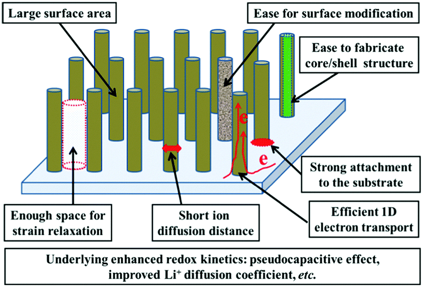
Such redox-based optical response makes nanostructuring an effective approach to boost the electrochromic performance. The preparation of the electrochromic materials directly grown on TCO substrates (“self-supported” electrodes) is rather favorable for electrochromism due to the elimination of the incorporation of conductive additives or electrode binders and the added step of slurry casting during the electrode fabrication process.15,16 Furthermore, the formation of 1D nanoarchitectures, such as nanoneedle, nanorod, nanofiber, nanowire, and nanotube arrays, could significantly improve the electrochromic performance due to the electrochemical superiorities of these morphologies.6–8,17 Thus, the synthesis of 1D nanomaterials employing a self-supported strategy has become fascinating for electrochromism. Self-supported 1D nanostructures possess the general nanostructure-derived electrochemical and electrochromic advantages such as large surface area providing plenty of accessible electroactive sites for high coloration contrast, short ion diffusion distance for fast switching response, and enough voids for efficient strain relaxation, etc., while self-supported 1D nanoarchitectures also demonstrate several unique electrochemical and electrochromic advantages. Fig. 1 shows a schematic representation of an idealized self-supported 1D electrode.
 | ||
| Fig. 1 Schematic diagram illustrating the advantages of an ideal self-supported 1D nanostructure for electrochromism. | ||
(i) Controllable areal density of the electroactive materials: the loose stacking of electroactive materials is particularly important for electrochromic electrode films because of the favorable electrolyte penetration and enough voids for strain relaxation. On the other hand, the ideal areal density of the electrode materials is a key factor to realize high electrochromic performance. Low areal density of electroactive materials could give rise to unsatisfactory coloration contrast while too high areal density of electroactive materials might result in slow redox kinetics. For the majority of methods used to synthesize self-supported 1D nanomaterial films, the areal density of the electroactive materials can be facilely controlled.18–20
(ii) Strong attachment to the substrate and efficient 1D electron transport: for the majority of methods used to fabricate self-supported 1D nanostructured films, the electrochromic materials are directly grown on substrates, resulting in strong physical and chemical attachment between the electroactive materials and substrate, as well as continuous conductive pathways to the substrate, guaranteeing efficient electron transport for electrochromism. In addition, strong bonds ensure the structural integrity of the whole electrode films, efficiently preventing the detachment of electrochromic materials from the substrate, beneficial for the long-term cycling performance.
(iii) Underlying enhanced redox kinetics: due to their structural advantages, the majority of delicately designed self-supported 1D nanostructures can exhibit enhanced redox kinetics, compared to bulk and many other nanostructured materials. Because of efficient 1D electron transport, large surface area, and other characteristics such as a large number of surface defects which are formed during the preparation process or post-treatment, the kinetics of redox reactions occurring on the surface and near surface layer are significantly improved. Such fast redox kinetics leads to an enhanced pseudocapacitive effect which is beneficial for fast switching response. An enhanced surface contribution has been found in electrode films of self-supported nanofiber,21 nanorod22 and nanotube arrays.23 In addition, for some delicately designed self-supported 1D nanostructures, their ion diffusion coefficient and electronic conductivity also can be significantly improved due to the surface defects, guest ion doping and single-crystal nature of the nanofibers and nanorods.24 Furthermore, some studies demonstrate that 1D nanostructures also exhibit a short characteristic relaxation process, indicating the high electrochemical stability of redox states in 1D nanostructures.25
(iv) Ease of realizing the surface modification or fabrication of hybrid nanostructures: reactive liquids and gases (such as hydrogen, ammonia, and plasma) can easily penetrate and flow in the interconnected voids among the nanofibers or nanorods. Then reactions occur and may lead to mixed valences, new phases, defects, changes in the band structures, and/or production of new functional groups on the surfaces of the materials.
Using pre-prepared self-supported nanofibers and/or nanorods as templates to deposit another electrochromic material gives rise to self-supported core/shell hybrid nanostructures, which could exhibit enhanced coloration contrast and cycling stability, shortened switching response time, and increased coloration states. The coating layer can be the same material as that of the core but in a different phase, generating a “crystalline/amorphous core/shell” nanostructure.26 However, in most cases, the coating material is different from that of the core.27 As for the anodic preparation method, mixed metal oxides or doped nanotube arrays can be facilely prepared from anodization treatment on alloys.
(v) Ease of characterization and assembly of electrochromic devices: the strong structural integrity of self-supported 1D nanostructured electrode films indicates that these films can be directly used for electrochemical-optical characterization or device assembly.
(vi) Ease of realizing multifunctional electrodes or devices. Both electrochemical energy storage and electrochromism are from redox reactions, causing bifunctional integration into one film or device to be possible.28,29 However, the existing conflicts between electrochromism and electrochemical energy storage (such as fast switching response for electrochromism and high energy density for electrochemical energy storage) result in the necessity of delicately designed nanostructured morphologies. Fabrication of self-supported 1D nanostructures with high ion insertion/extraction kinetics is an ideal approach to solve these problems, as described in later sections. Furthermore, given the significance of self-supported 1D nanostructures for the emerging miniaturization of power sources aimed at integration into micro- and nano-electronic devices,8 fabrication of such self-supported 1D morphologies is becoming more and more vital and important for miniaturized electrochromic energy storage devices.
4. Template-derived self-supported 1D nanostructures for electrochromism
Employing porous templates is a direct and effective method to prepare nanostructures for high-performance electrochemical-optical materials. The general fabrication process of nanostructures relies on the replication of the well-confined voids (such as holes, pores, channels or other hollow spaces) of the templates.18,30 Various methods, for instance electrodeposition, sol–gel chemistry, hydrothermal deposition, and physical/chemical vapor deposition have been developed to effectively fill the voids with precursors. Removing the templates and transforming the precursors into the targeted materials with post treatments produces the replicated nanostructures. The large variety of templates with diverse porous morphologies can produce various nanomaterials from 1D nanostructures (nanofibers, nanorods, nanotubes, etc.) to 3D ordered or disordered meso-/macro-porous materials. Also, some biological species (such as leaves, butterfly wings, wood, viruses, proteins, and DNA) are used as templates to form nanowires and other nanostructures.31The templates widely used to fabricate self-supported 1D nanostructures are membranes with 1D parallel nanochannels. There are two types of typically used templates: polymetric (such as PC and nitrocellulose) and oxide-based (AAO) membranes. Their high pore density (up to 1011 cm−2) and wide pore diameter range (from tens to hundreds of nanometers) could ensure membrane-derived self-supported 1D nanostructures with a desirable areal density of electroactive materials, a controlled diameter scale and enough interspacing voids for efficient electrolyte penetration to achieve satisfactory coloration saturation. Meanwhile, the large thickness range of the membranes (from several to hundreds micrometers) gives feasible choice to prepare 1D nanostructures with controlled length.
4.1 Template-derived self-supported 1D metal oxide nanostructures
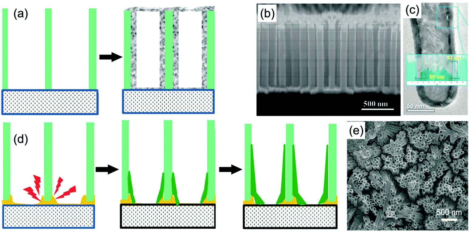
Typical membrane-assisted preparation of metal oxide self-supported nanofiber and nanorod arrays is shown in Fig. 2a. Attaching the template to the TCO substrate, filling the nanochannels with precursors and then transforming them into the targeted metal oxides with subsequent annealing treatment whilst removing the membrane leads to the successful synthesis of self-supported metal oxide nanorod, nanowire, or nanofiber arrays (Fig. 2b).30 The tight attachment of the membrane to the substrate could effectively ensure strong physical and chemical contacts between the electroactive materials and the TCO substrate, resulting in efficient electron transport and long-term cycling stability. Meanwhile using different experimental details can control the morphologies of the 1D nanostructures, simply from nanorod arrays to nanofiber arrays. Notably, when the mechanical strength of the targeted 1D electroactive materials is not high enough or the length-to-diameter ratio of the targeted 1D electroactive materials is rather high, the tops of the nanorods or nanofibers could aggregate together, forming nanorod or nanofiber bunches instead of free standing and isolated nanorod or nanofiber arrays. | ||
| Fig. 2 (a) Schematic diagram illustrating the template-assisted synthesis of self-supported 1D metal oxide nanostructures. Step 1 is attachment of membranes on the TCO substrates, followed by a precursor filling process. Step 2 is the removal of the membranes and transformation of the precursor into the targeted metal oxide. (b) SEM image of TiO2 nanorod arrays prepared using an AAO membrane. Reprinted from ref. 30. Copyright 2015 Springer. (c and d) SEM image of open-ended (nanorod bunches) and close-ended Ni(OH)2 nanorod arrays prepared using an AAO membrane. (e) Comparison of the transmittance modulation for the annealed Ni(OH)2 thin film, and close-ended and open-ended nanorod structures. Reprinted from ref. 35. Copyright 2014 Wiley. | ||
Zheng et al. prepared arrays of WO3 nanorods with lengths of ca. 1.8 μm by direct current (DC) magnetron sputtering of WO3 on an aluminum lattice membrane (an AAO membrane with short thickness).32 The confined growth of WO3 in the 1D nanochannels led to the diameter of the self-aligned parallel WO3 nanorods being almost the same as the pores of the aluminum lattice membrane (about 200 nm). In 1 M NaCl solution, sodium-ion insertion under −0.8 V (vs. SCE) led to blue coloration, while bleaching under 1.2 V polarization resulted in a transparent state. The WO3 nanorod arrays demonstrated obvious transmittance modulation in the visible spectrum range with a maximum value of about 50% at λ = 600 nm. By using a two-step-oxidation prepared AAO membrane with a pore size of 80 nm as a template and a colloidal suspension as a precursor, arrays of WO3 nanorods with nanosized pores distributing regularly along the length of the nanowires were prepared.33 A two-step electrochemical anodization on Al–W overlapped metal layers to prepare Al-doped WO3 nanorod arrays was proposed by Park et al.34 The outer Al layer was anodized into AAO, followed by anodization of the W layer creating Al-doped WOx in the pre-formed nanochannels of AAO. The removal of the AAO template and annealing treatment produced self-supported nanorod arrays on a W substrate. With the assistance of AAO membranes on ITO substrates, Guo et al. prepared two types of self-supported Ni(OH)2 nanorod arrays by electrodeposition filling and removal of the membranes with 10% NaOH solution. Over deposition gave rise to a dense film on the top of the nanorod arrays, producing a close-ended morphology (Fig. 2c and d).35 Open-ended nanowire arrays demonstrated good electrochemical activity with superior transmittance modulation of ∼35% at λ = 635 nm, better than the close-ended nanowire arrays and dense film (∼20% and 17%, respectively) (Fig. 2e). Also, by comparison with other literature reports, the authors also found that the open-ended nanowire arrays exhibited higher coloration efficiency (50.5 cm2 C−1) than many other Ni(OH)2 nanostructures, further demonstrating the efficient redox kinetics for low energy consumption in electrochromic nanowire arrays. Yamada et al. used a two-step process to prepare branched Au/NiO nanorod arrays for accelerated electrochromic color changes.36 After Au nanorod arrays were prepared by AAO membrane-assisted electrodeposition, a branched NiO layer was deposited on the Au surface. Due to the high reflectivity, mechanical strength and electrical conductivity of Au, as well as the thin thickness of the NiO layer (15 nm), the branched Au/NiO electrode exhibited high and stable reflectance contrast over 0.4 at λ = 600 nm.
Polymetric membranes (PC membrane as representative) are another category of widely used templates to prepare self-supported 1D nanostructures. The preparation process also can be reflected in Fig. 2a. These polymetric membranes can be easily wiped out by annealing treatment in air or dissolution by organic solvents. Limmer et al. demonstrated a general technique to synthesize metal oxide nanorod arrays using sol electrophoretic deposition with appropriate track-etched hydrophilic PC membranes attached on the ITO substrates.37,38 Electrochromic TiO2, V2O5, and Nb2O5 polycrystal nanorods with diameters of ∼100 nm and a length of ∼10 μm were prepared. These oxide nanofiber arrays exhibited absorbance modulation in the visible spectrum range with obvious color contrast during the Li-ion insertion/extraction processes. Furthermore, Limmer et al. also found that the diameter of the V2O5 nanorods can decrease to 50 nm; meanwhile these nanorods were changed to be single crystals by using delicately designed experimental parameters.39 These single-crystal V2O5 nanorod arrays exhibited higher transmittance modulation and faster switching response speed compared to polycrystal V2O5 nanorod arrays and a sol–gel-derived V2O5 dense film. Li-ion storage properties detected by charge/discharge tests showed that single-crystal V2O5 nanorod arrays exhibited superior lithium storage.39,40 Higher lithium storage of the single-crystal V2O5 nanorod arrays confirmed their electrochromic advantages because the larger amount of inserted Li-ions indicated that a larger amount of V5+ ions took part in the redox reactions for electrochromism. Furthermore, compared to the polycrystalline V2O5 (10−3–10−2 S cm−1), the high electrical conductivity of single-crystal V2O5 nanofibers (0.5 S cm−1)41 positively influenced the Li-ion insertion/extraction kinetics, which was beneficial for improving the electrochromic performance. By using PC membrane-assisted sol electrophoretic deposition, single-crystal TiO2 nanofiber arrays were also prepared.42 Furthermore, self-supported mixed transition metal oxide nanorod or nanofiber arrays, such as V2O5–TiO2,43 can also be prepared using a mixed metal oxide sol solution. Self-supported 1D nanostructures of mixed transition metal oxides were believed to possess better electrochromic performance compared to the corresponding 1D nanostructures of a single metal oxide component, because of the multiple types of color centers and enhanced redox kinetics derived from doping effects.
Nanotube arrays are another type of self-supported 1D nanostructure that can be prepared using PC and AAO membranes. Compared to nanofiber and/or nanorod arrays, nanotube arrays exhibit several electrochemical advantages. The internal cylindrical pores not only significantly increase the amount of surface electroactive sites to enhance optical modulation, but also obviously decrease the ion diffusion distance to improve the switching response speed, as well as provide more voids for efficient strain relaxation.18,44,45 In addition, for metal oxide nanotubes, the crystal size of the electroactive materials is usually smaller than that of nanofibers or nanorods, which is believed to be feasible for ultrafast redox kinetics.18
The uniformly preferential growth of metal oxide precursors on the surface of nanochannels is a prerequisite for synthesizing nanotubes employing PC or AAO membranes. Atomic layer deposition (ALD) combining AAO membranes is a well-developed process to prepare self-supported metal oxide nanotube arrays.46,47 In an ALD process, the gaseous precursors travel into the voids of the membrane and are preferentially absorbed on the surface of the nanochannels to decrease the system energy, producing nanotubes attached on the surface of the nanochannels (Fig. 3a). Furthermore, a surface layer covering on the membrane is usually produced in the ALD process. The removal of the membrane and the surface layer produces metal oxide nanotube arrays. Fig. 3b and c demonstrate typical SEM and TEM images of TiO2 nanotube arrays prepared by the approach combining an AAO template and ALD.46 The capability to prepare perfectly ordered nanotube arrays with a uniform pore size, length and wall thickness through the entire film is an outstanding advantage of this method. On the other hand, further excessive deposition of precursors in the nanochannels could make the voids fully filled, producing nanorod or nanofiber arrays. Preparation of nanotube arrays employing low concentration of metal oxide sol solution and AAO membranes is also due to the preferential absorption of colloid particles on the surface of the nanochannels.44,48 Physical and chemical interactions between the metal oxide sol solution (precursors) and the templates, such as capillary forces, hydrophobic interactions and chemical bonds could also enable the successful preparation of nanotubes. These chemical and physical interactions were also the main forces for the production of nanotubes during the filling process of membranes using hydrolysis49 and layer-by-layer (LBL) coating50 methods.
 | ||
| Fig. 3 (a) Schematic diagram illustrating metal oxide nanotube arrays prepared using a membrane-assistant ALD process. (b and c) SEM and TEM images of TiO2 nanotube arrays prepared by the approach combining an AAO template and ALD method. Reprinted from ref. 46. Copyright 2015 American Chemical Society. (d) Schematic diagram illustrating metal oxide nanotube arrays by using a membrane-assistant electrodeposition process. A sputtered Au layer is used as a conductive binder between the membrane and substrate. (e) SEM image of TiO2 nanotube arrays prepared from an AAO template-assisted electrodeposition method. Reprinted from ref. 52. Copyright 2014 American Chemical Society. | ||
Electrodeposition with the assistance of PC and AAO membranes under constant current density is another well-developed approach to fabricate self-supported metal oxide nanotube arrays. Because of the insulated characteristic of the membranes, a conductive layer needs to be coated on one surface of the membrane as a substrate to realize electrodeposition. Usually, a thin gold layer is sputtered or evaporated on the surface of the membrane to produce a conductive substrate. Researchers found that the deposition speed around the joint sites between the membrane and substrate was faster than other positions, which finally created nanotube arrays after the removal of the membrane (Fig. 3d).51–53 A rational theory explaining the fast growth speed was the high electric field around the joint sites. Additionally, by-products produced during the electrodeposition, such as H+, OH−, and hydrogen bubbles, could also be beneficial factors for producing nanotubes. Fig. 3e shows the SEM image of TiO2 nanotube arrays prepared by an AAO membrane-assisted galvanostatic deposition process.52 The bottom-up growth of TiO2 led to nanotube arrays tightly bonded to the substrate; while uniform current density on the whole substrate ensured that the nanotubes showed relatively uniform diameter and length. In addition, when the deposition time is enough long or the deposition current density is rather high, excessive deposited metal oxide could be filled in the nanochannels, resulting in nanorod or nanofiber arrays.
Other 1D nanostructures, such as carbon nanotube arrays54 and ZnO nanorod arrays55 could also be used as templates to prepare metal oxide nanotube arrays. Notably, the mechanism using ZnO nanorod arrays as templates to prepare metal oxide nanotube arrays was sacrificial template-accelerated hydrolysis, a process of gradual dissolution of ZnO and slow deposition of amorphous metal oxide particles on the surface of the nanorods. The nanotubes prepared by this hydrolysis process were mesoporous and composed of several nanometer-sized crystals, leading the as-prepared nanotube arrays to demonstrate high optical modulation and fast switching response, as well as high-rate Li-ion storage, as shown in the following part about electrochromic energy storage devices.
Until now, scattered studies about the use of template-derived self-supported metal oxide nanotube arrays for electrochromism have been reported. However, it is believed that these nanostructured electrodes are desirable for high electrochromism because they have exhibited highly reversible and stable redox kinetics as reflected by the high-rate and long-term electrochemical energy storage performance.56,57
4.2 Template-derived self-supported 1D conductive polymer nanostructures
Self-supported 1D conductive polymer nanostructures can also be fabricated employing PC and AAO membranes. The preparation process of these conductive polymer 1D nanostructures is similar to the synthesis process used to fabricate transition metal oxide 1D nanostructures. Electropolymerization is widely used to fill the nanochannels due to the advantages of bottom-up growth and ease of producing uniform conductive polymer 1D nanostructures. Similar to the AAO membrane-assisted electrodeposition of metal oxides, conductive polymer nanorod (or nanofiber) and nanotube arrays can be selectively synthesized by controlling the experimental parameters.58Fig. 4a and b demonstrate SEM images of self-supported PPy nanofiber59 and poly(3-methylthiophene) nanotube60 arrays prepared by AAO membrane-assisted electropolymerization, respectively.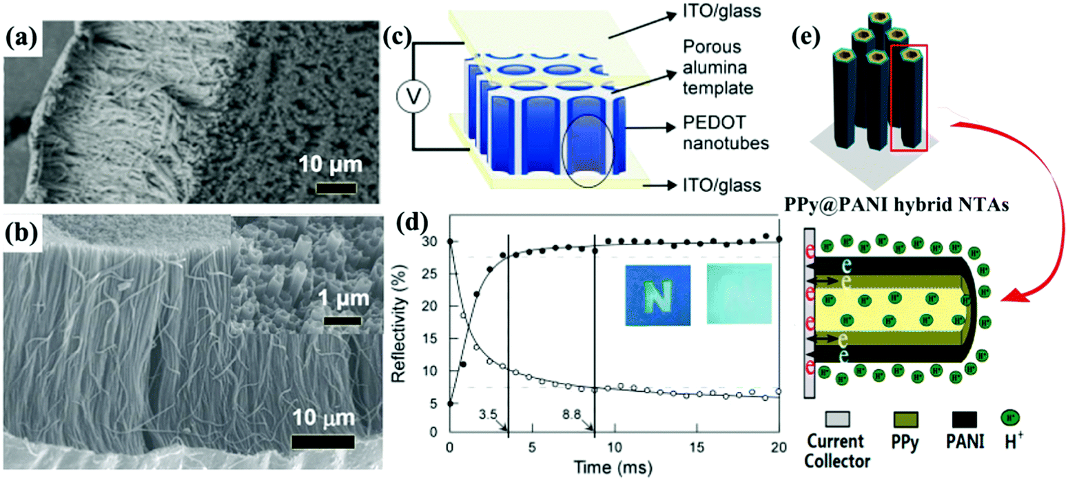 | ||
| Fig. 4 (a) SEM image of PPy nanofiber arrays prepared by AAO-membrane assisted electropolymerization. Reprinted from ref. 59. Copyright 2016 by Wiley. (b) SEM image of poly(3-methylthiophene) nanotube arrays prepared by AAO-membrane assisted electropolymerization. Inset top-view SEM image indicating the hollow character. Reprinted from ref. 60. Copyright 2016 by Elsevier. (c) Schematic representation of an ultrafast electrochromic device based on PEDOT nanotube arrays. (d) Plots of reflectivity of the PEDOT electrochromic window monitored at λ = 530 nm for coloration and bleaching. Patterned letter “N” on the device to demonstrate the color contrast between coloration and bleaching states. Reprinted from ref. 65. Copyright 2005 by Wiley. (e) The nanotube array architecture, double-walled structure, and high conductivity in the electrode provide ion and electron “highways” and a high utilization rate of the electrode. Reprinted from ref. 80. Copyright 2013 American Chemical Society. | ||
Besides the above mentioned electrochemical advantages of the nanostructures, 1D nanostructuring can give the conductive polymers two interesting merits for electrochromism. (1) It was found that the nanofibers and nanotubes fabricated with AAO membranes demonstrated higher electric conductivity than dense films, and the value increased with the decrease of the diameter for nanofibers (or nanorod, and nanowire) or the wall thickness for nanotubes.61 For example, detected by using four-probe technology on platinum micro-electrodes, when the diameter of PEDOT nanofibers decreased from 190 to 25 nm, the electric conductivity increased from ca. 11 to 550 S cm−1.62p-Toluene sulfonic acid doped PPy microtubes with 560–400 nm outer diameters exhibited poor conductivity of only 0.13–0.29 S cm−1 (the inner pore diameter was 80 nm), while a high conductivity of 73 S cm−1 was achieved when the outer thickness was about 130 nm.63 Research implied that confined growth in the narrow nanochannels of the membranes altered the extent of disorder and polarons on the main chains of the conductive polymers, resulting in high electrical conductivity.61–63 (2) The AAO membrane-derived conductive polymer 1D nanostructures demonstrated enhanced mechanical strength due to the extent of arrangement of the conductive polymer main chains.61 For instance, research indicated that PPy nanotubes with thicker walls demonstrated higher elastic modulus.64 When the PPy nanotube thickness was between 20 and 16 nm (outer diameter of nanotube: between 100 and 70 nm), the elastic modulus of a single nanotube was around 5 GPa. When the nanotube wall thickness decreased under 16 nm (outer diameter of nanotube: <70 nm), the elastic modulus strongly increased with decreasing wall thickness. It reached a value close to 60 GPa for a thickness of 6.5 nm (outer diameter of nanotube: 35 nm). The high electric conductivity and mechanic strength are beneficial for fast electrochromic redox kinetics and long-term cycling performance.
Because of the intrinsic fast redox kinetics of conductive polymers and short ion diffusion distance, conductive polymer nanotube arrays could demonstrate fast color and optical switching response under a voltage stimulus. Fast color switching is a prerequisite, especially for display applications. The desired video rate of movies for human eyes is about 24 frames per second, i.e. about 42 ms to accomplish color switching is the minimum requirement. Fig. 4c illustrates arrays of electropolymerized PEDOT nanotubes attached on the inner wall surface of an AAO membrane for reflectance-mode electrochromic cells.65 The AAO membrane was not removed to maintain the well-ordered arrangement of the nanotube arrays. Because of the short ion diffusion distance of the nanotube walls, these PEDOT nanotube arrays demonstrated fast redox doping/de-doping (bleaching/coloration) speeds with rapid switching of ca. several milliseconds to fulfill reflectivity modulation of ca. 23% at λ = 530 nm, as well as strong coloration contrast (between colorless and blue, contrast of 6) (Fig. 4d). The fast switching response and strong coloration contrast meant that the as-prepared PEDOT nanotube arrays could be used for display applications. In contrast, the PEDOT dense films exhibited a rather long switching response time of 1–2 s because of long ion diffusion distance.66 By using a PC membrane attached on an Au/Cu bilayer metal foil and dissolving it after electropolymerization, Cho et al. prepared flexible reflectance-mode PEDOT electrochromic electrodes.67 Although the removal of the membrane made some nanotubes become curved and fall down, resulting in a somewhat unexpected adverse influence on the electrochromic performance, this flexible electrode still demonstrated fast switching responses (20 and 30 ms for bleaching and coloration processes, respectively) with high reflectivity modulation of ca. 50% at λ = 600 nm. Attaching an AAO membrane on an ITO substrate and dissolving the template after electropolymerization produced PEDOT nanotube array electrodes for window-mode electrochromic devices.68 The as-prepared PEDOT nanotube arrays showed obvious transparent/blue color contrast and high transmittance modulation of 45% at λ = 600 nm during the electrochemical doping/de-doping switching cycles. However, compared to the Au/Cu bilayer metal foil substrate, the relatively low electric conductivity of the FTO substrate resulted in slightly increased response times (50 and 70 ms for bleaching and coloration, respectively). Nanofiber, nanorod, and nanotube arrays of other conductive polymers (such as PANI, PPy and PT) for electrochromism were also successfully prepared by electropolymerization with AAO and PC membranes.69–71
Liquid crystals,72 porous block copolymer films,73 Au nanorod arrays,74 silicon nanowire arrays,75 nanopatterned polydimethylsiloxane (PDMS) molds,76 anodic metal oxide nanotube arrays,77 ZnO nanorod arrays,78 and MnO2 nanostructures79 have also been used to fabricate self-supported conductive polymer 1D nanostructures with high electrochemical and electrochromic performance. In particular, the ZnO nanorod arrays were also used to fabricate mixed conductive polymer double-walled nanotube arrays (PPy@PANI hybrid NTAs) (Fig. 4e).80 The PPy@PANI hybrid NTAs exhibited extraordinarily higher electrochemical activity and stability compared to the nanotube arrays with a single component due to the underlying synergistic effect.81,82 Such mixed double-walled nanotube arrays bring interesting insights into the design of nanostructures for electrochromism.
5. Template-free self-supported 1D nanostructures for electrochromism
5.1 Solution process-deposited self-supported 1D metal oxide nanostructures
Solution deposition is one of the most widely used methods to fabricate electrochromic self-supported 1D metal oxide nanostructured electrodes. In a typical synthesis, a TCO substrate is immersed into a solution containing precursors. With thermodynamics and kinetics activations, metal oxide nuclei are produced at the low energy sites of TCO substrates. After enough time to fulfil crystal growth, self-supported 1D metal oxide nanostructures on TCO substrates are obtained. A subsequent annealing treatment is used to make the as-prepared metal oxides crystallized if fully crystalline samples are required. By varying the experimental details, the thickness of the nanostructured films and the areal density of the electrode materials could be optimized for high optical modulation and fast switching response. In particular, when used for transmittance-mode electrochromic devices, as-fabricated electrode films with high transparency are greatly expected because of the enhancement of the bleaching/coloration contrast.4,5The solution process-based preparation process of self-supported 1D metal oxide nanostructures typically includes two types: hydrothermal and ambient pressure methods. Hydrothermal (or solvothermal when the solvent is not water) growth of metal oxides on substrates usually operates in a sealed autoclave above ambient temperature (typically from 120 to 200 °C) in a solution with metal-element-containing precursors (such as metal salts and organometallic compounds). Using a suitable synthesis temperature and pressure, fully crystallized even single-crystal metal oxide nanostructures could be produced, so post heat treatment is often not necessary. The hydrothermal method possesses many advantages including: (1) relatively lower temperature than that of solid reactions; (2) ease of preparing single phase nanomaterials; (3) ease of preparing various morphologies by simply using different tunable experimental parameters, such as temperature, type and concentration of the precursors, and solvents; (4) ease of preparing uniformly doped materials. However, the high sensitivity of the morphology and phase of the products on the experimental details as well as the still not fully understood nanostructure growth mechanism under hydrothermal processes could bring some difficulties for the reproduction of the morphology and/or performance. Furthermore, the relatively not large volume of autoclaves may limit the areal size of the as-synthesized electrodes, which could bring some unpleasant difficulties for practical applications.
An ambient pressure solution processes to prepare nanostructures are conducted in open vessels. Similar to the hydrothermal process, metal oxide nanostructures are also deposited on the TCO substrates from the metal-element-containing precursor solution, but the synthesis temperature under ambient pressure is lower than that of the hydrothermal method due to the limitation of the boiling point of the solvents. The growth of metal oxide nanostructures in an ambient pressure solution process is derived from the hydrolysis of metal ions in the solution or crystallization process of the sol–gel-based solution. In addition, the as-deposited nanostructures usually either contain crystallographic and/or absorbed water, or are amorphous and poorly crystallized, or are metal hydroxides, indicating that a subsequent annealing is needed. However, nanostructured electrodes with a large size can be facilely prepared using an ambient pressure solution process because of no requirement on the high experimental temperature and pressure as well as the size of experimental vessels. In addition, flexible electrochromic film electrodes can be prepared using an ambient pressure solution method, because typically used flexible transparent conductive substrates are polymer films (such as polyethylene terephthalate (PET)) coated by ITO or FTO layers. These flexible substrates are not stable under hydrothermal and solid state reaction conditions.
Tungsten oxide. Tungsten oxide (WOx) is one of the most common transition metal oxides used to hydrothermally fabricate self-supported 1D nanostructures for a high cathodic electrochromic electrode. Crystalline WOx materials are a category of oxide with perovskite-like structures mainly formed with WO6 octahedra arranged in various corner-sharing or edge-sharing configurations.3,10 Theoretical calculations on the electronic structures of WO3 and MxWO3 (M = H, Li, Na) demonstrated that the electrochromism of WOx was from small-ion insertion-derived band changes which had a strong relationship with the changes of oxygen ions of W–O–W bridges.3,83,84 Depending on the different hydrothermal conditions for crystal growth, WO6 octahedra can be organized in various sharing (edges, corners and planes) configurations in different tilting angles and distortions, generating a variety of WOx materials with different phases and/or W
![[thin space (1/6-em)]](https://www.rsc.org/images/entities/char_2009.gif) :O stoichiometric ratios, such as tetragonal WO3, orthorhombic WO3, monoclinic WO3, triclinic WO3, cubic WO3, W3O8, and W18O49.83 Although the electrochromic color changes of these WOx materials are the same (between blue and transparent), WOx materials with different phases exhibit different electron band structures and lattice void types, giving rise to different ion insertion/extraction kinetics which leads to different optical modulation and switching response speeds. In addition, using different hydrothermal parameters can produce various self-supported WOx nanostructured morphologies with high research significance. These morphologies include basic 1D nanostructures (such as nanorod,85–88 nanofiber89–93 and nanoribbon94–96 arrays), complex 1D nanostructures (such as nano-/micro-flowers,97,98 nanoforests,99,100 honeycomb-like nanostructures,101,102 and nest-like nanostructures103) and other nanostructures (such as nanosheet,104–106 nanobricke,107 nanoplate,108,109 and nanocuboid110,111 arrays). Fabricating WOx nanostructures with different phases and/or morphologies then investigating their electrochemical-optical performance is meaningful for not only the theoretical study of the hydrothermal crystallization mechanism and redox kinetics of WOx, but also the promotion of practical application of nanostructured WOx. Electroanalysis exhibited that self-supported 1D WO3 nanostructures showed superior redox kinetics, including improved lithium-ion diffusion coefficient and enhanced pseudocapacitive effect which were beneficial for electrochromism.84,109
:O stoichiometric ratios, such as tetragonal WO3, orthorhombic WO3, monoclinic WO3, triclinic WO3, cubic WO3, W3O8, and W18O49.83 Although the electrochromic color changes of these WOx materials are the same (between blue and transparent), WOx materials with different phases exhibit different electron band structures and lattice void types, giving rise to different ion insertion/extraction kinetics which leads to different optical modulation and switching response speeds. In addition, using different hydrothermal parameters can produce various self-supported WOx nanostructured morphologies with high research significance. These morphologies include basic 1D nanostructures (such as nanorod,85–88 nanofiber89–93 and nanoribbon94–96 arrays), complex 1D nanostructures (such as nano-/micro-flowers,97,98 nanoforests,99,100 honeycomb-like nanostructures,101,102 and nest-like nanostructures103) and other nanostructures (such as nanosheet,104–106 nanobricke,107 nanoplate,108,109 and nanocuboid110,111 arrays). Fabricating WOx nanostructures with different phases and/or morphologies then investigating their electrochemical-optical performance is meaningful for not only the theoretical study of the hydrothermal crystallization mechanism and redox kinetics of WOx, but also the promotion of practical application of nanostructured WOx. Electroanalysis exhibited that self-supported 1D WO3 nanostructures showed superior redox kinetics, including improved lithium-ion diffusion coefficient and enhanced pseudocapacitive effect which were beneficial for electrochromism.84,109
Fig. 5a demonstrates typical SEM images of hydrothermally prepared WO3 arrays of nanorods with a typical diameter of ∼80 nm and length of ∼1.1 μm on an FTO substrate.86 Investigation of the morphology changes in the samples sequentially prepared under different reaction times indicated the WO3 nanorod array growth mechanism. It was found that the substrate provided low energy sites for nucleation, and the shape of the initially grown WO3 nanocrystals was irregular. With further growth, these irregular nanocrystals transformed into a rod shape to expose the low energy crystal faces to decrease the system energy. It was also noteworthy that the initial generated small WO3 nanorods randomly stacked on the substrate, but the nanorods which were not perpendicular to the substrate were dissolved with the increase of experimental time also due to a decrease of system energy, finally producing WO3 nanorod arrays grown on the FTO substrate, as shown in the inset cross-sectional view SEM image. Arrays of WO3 nanorods with a diameter of ∼22 nm and length of ∼240 nm prepared using similar hydrothermal parameters exhibited a high transmittance modulation of 41.2% at λ = 632.8 nm and fast switching responses (3.6 s for coloration and 4.2 s for bleaching).87 Using substrates with pre-deposited WOx seeds is another efficient hydrothermal method to grow WO3 nanorod arrays.85,88 It exhibits several advantages, including controllable areal density of nanomaterials and more uniformly produced morphology. A seed-based cylindrical WO3 nanorod array film exhibited a large transmittance modulation of 66% at λ = 632.8 nm and a high coloration efficiency of 106.8 cm2 C−1.88
 | ||
| Fig. 5 (a) SEM images of self-supported WO3 nanorod arrays. Reprinted from ref. 86. Copyright 2013 by Royal Society of Chemistry. (b) SEM images of self-supported WO3 nanofiber arrays. Reprinted from ref. 92. Copyright 2014 Elsevier. (c) SEM images of self-supported W18O49 nanofiber arrays. Reprinted from ref. 93. Copyright 2016 Royal Society of Chemistry. (d and e) SEM image and electrochromic performance of a nanofiber stacked honeycomb WO3 architecture. Reprinted from ref. 101. Copyright 2015 Royal Society of Chemistry. | ||
Self-supported WO3 nanofiber arrays were also prepared as electrochromic electrodes. Fig. 5b demonstrates typical SEM images of WO3 nanofiber arrays on an FTO substrate prepared in hydrothermal solution containing similar reagents to that used to prepare nanorod arrays.92 The production of nanofibers can be regarded as the further growth stage of nanorods. As discussed above, the preferred orientation leads to the growth of nanorods along the length direction being faster than that along the diameter direction, finally giving rise to a nanofiber array morphology. The as-prepared WO3 nanofiber arrays showed remarkable enhancement of the transmittance modulation in the visible spectrum (66.5% at λ = 633 nm) and IR region (73.8% and 57.7% at λ = 0.2 and 8 μm, respectively), as well as high cycling stability. To further improve the length-to-diameter ratio, especially decrease the scale of the diameter, chemicals restricting the growth along the diameter direction were added to the hydrothermal solution. For instance, Zhang et al. developed a sulfate-assisted hydrothermal method to prepare arrays of WO3 nanofibers with a long length of ∼1.5 μm with a small diameter of 20–40 nm.90 The as-prepared nanofiber films exhibited a high coloration efficiency of 102.8 cm2 C−1 and fast switching speeds (7.6 and 4.2 s for coloration and bleaching, respectively). Employing mixed solvents or pure organic solvent was another effective method to prepare nanofibers with high length/diameter ratio. Hung et al. prepared nanofiber network films on an FTO substrate in a water/isopropyl alcohol mixture solution.91 The fast Li-ion insertion/extraction kinetics with a Li-ion diffusion coefficient of 2.14 × 10⁻⁹ cm2 s−1 led to a desirable transmittance modulation of 57% at λ = 632 nm and a high coloration efficiency of 120.3 cm2 C−1. A solvothermal process seems to be more favorable to synthesize tungsten oxide nanofibers with a smaller diameter. Lu et al. prepared W18O49 nanofiber arrays with diameter <25 nm in polyethylene glycol as a solvent.89 The as-prepared W18O49 nanostructures exhibited a high transmittance modulation of 49.64% at λ = 632.8 nm with high cycling stability (>3000 cycles). Lu et al. found that the solvothermal preparation in methanol solvent could further downsize the diameter of W18O49 nanofibers to ∼6 nm (Fig. 5c).93 A complementary electrochromic device based on self-supported W18O49 nanofiber arrays and a Prussian blue thin film showed a high transmittance contrast (59.05% at λ = 632.8 nm) and fast switching response (coloration time of 6.9 s and a bleaching time of 1.2 s). A nanofiber stacked honeycomb WO3 architecture with high Li+ diffusion coefficient of 3.091 × 10⁻⁹ cm2 s−1 was prepared by using a seed and sulfate co-assisted hydrothermal process (Fig. 5d).101 A assembled half-cell electrochromic device (bare TCO substrate as counter electrode) exhibited continuous color changes with high optical modulation of 60.74% at λ = 630 nm and fast switching response time (4.29 s for coloration and 3.38 s for bleaching) (Fig. 5e).
Titanium oxide. Titanium oxide (TiOx) is a type of cathodic electrochromic material with color changes between blue (coloration) and transparent (bleached). TiO2, the most common oxide type of hydrothermal or heat-treated product, has been regarded as a promising electrochromic material due to its stable crystal structure, low cost, high mechanical stability, environmental friendliness, safety, and fast charge transport and collection abilities.112,113 TiO2 naturally exhibits three common types of polymorphs, i.e., rutile, anatase, and brookite. All these three TiO2 phases use Ti–O octahedrons as the fundamental building block and share hollow lattice channels for facile ion (H+ and Li+) insertion/extraction. In addition, the significantly improved electron diffusion coefficient114,115 and enhanced surface redox contribution116 in TiO2 nanorods and nanofibers make the hydrothermally fabricated TiO2 self-supported 1D nanostructures expected to be high-performance electrochromic electrode films.
Using delicately designed experimental parameters, Liu et al. reported a three-step hydrothermal process to prepare arrays of TiO2 single crystalline anatase nanofibers oriented in the [100] direction with a diameter of 105 ± 10 nm and length of 12.16 ± 0.56 μm on FTO substrates.117 Such [100] direction oriented nanofibers were believed to possess fast electron transport.112,113 Anatase TiO2 nanofiber arrays with a high-porosity cross-linked geometry directly grown onto FTO substrates were prepared through hydrothermal processes under mild alkali conditions.118 The TiO2 nanofiber array-based half-cell electrochromic device demonstrated a desirable transmittance change of 28.20% at λ = 600 nm and an acceptable coloration efficiency of 13.87 cm2 C−1 with fast switching response (11.3 s for coloration and 14.3 s for bleaching). Electroanalysis indicated that the enhanced Li+ diffusion coefficient is an important feature. In addition, a low refractive index of 1.37 made the as-prepared TiO2 nanofiber arrays become ideal electrode films for transmittance-mode electrochromic devices. Qiang et al. hydrothermally fabricated densely packed rutile TiO2 nanorod arrays on the FTO substrate.119 The high areal density of nanorods led the electrode film to exhibit large transmittance modulation in the visible spectrum range with a maximum value of approximately 64% at λ = 600 nm. Furthermore, a self-powered system integrating an electrochromic device and a dye-sensitized solar cell was also assembled and tested. To further improve the electrochromic performance, Liu et al. fabricated a micro-/nanostructured film of self-supported rutile TiO2 nanorod arrays decorated by anatase TiO2 nanoparticles (TiO2 NR-NP).120 This micro-/nano-structured film simultaneously possessed the high electron transport and mechanical stability properties from the nanorod arrays, and fast and reversible redox kinetics from the small decorated nanoparticles, giving rise to enhanced transmittance modulation as well as accelerated switching responses, compared to pure TiO2 nanorod arrays (TiO2 NR) (Fig. 6a). Using a two-step hydrothermal process and pre-fabricated self-supported TiO2 nanofiber arrays as skeletons, hierarchical TiO2 nanofiber arrays with densely-packed and omnidirectional branches were synthesized (Fig. 6b).121 A typical synthesis process was via high-concentration TiCl4 treatment of upright backbone TiO2 nanofibers to produce seeds on the surface followed by hydrothermal growth, giving rise to the growth of secondary TiO2 nanobranches (such as nanoneedles and nanosheets) on the TiO2 nanofiber backbone and in all directions (Fig. 6c). Such a preparation method brings new insights to prepare novel hierarchical nanofiber arrays where the nanofiber and nanobranches could be the same oxides or different types like WO3 nanostructures on a TiO2 nanofiber backbone. Hierarchical nanofiber arrays are desirable for electrochromic applications.
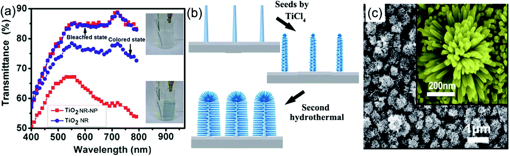 | ||
| Fig. 6 (a) Comparison of the transmittance modulation in the visible spectra of the TiO2 NW and NW-NP films. Inset figures demonstrate the coloration and bleaching colors of the TiO2 NW-NP film. Reprinted from ref. 120. Copyright 2014 Royal Society of Chemistry. (b and c) Schematic diagram illustrating preparation and SEM images of densely-branched TiO2 NWs. Reprinted from ref. 121. Copyright 2013 Royal Society of Chemistry. | ||
Nickel oxide and cobalt oxide. Nickel oxide (NiOx) and cobalt oxide (CoOx) are two representative anodic electrochromic metal oxides. Crystalline NiOx and CoOx are formed by NiO6 or CoO6 octahedra connected by sharing common corners and/or by sharing common edges.10 Because of the high electrical conductivity of NiOx and CoOx,122,123 as well as their stable lattice structure, crystalline NiOx and CoOx nanomaterials exhibit faster coloration/bleaching switching and higher cycling stability compared to many other electrochromic metal oxides.
NiO, the common electrochromic nickel oxide, has been widely investigated in alkali solutions. In electrochromic devices, NiO has been successfully explored as a competent anodic counter electrode (also called an ion storage electrode) in conjunction with WO3 as a cathodic working electrode.124 However, practical applications of NiO as a promising electrochromic material are still difficult because of the low color contrast, poor cycling durability and unsatisfactory ion storage capacity when the NiO is in bulk particles or a dense film. Fabrication of self-supported 1D NiO nanostructures on the TCO substrate is an ideal method to solve these problems. Typically, the initial hydrothermal crystalline products are hydrous nickel oxides or nickel hydroxides; an annealing treatment is needed to transform the hydrothermal products to NiO. However, because the initial generated hydrothermally synthesized crystalline products on TCO substrates were usually in morphologies of nanosheet arrays or nanosheet-stacked complex nanoarchitectures (such as rose-like), the annealing-produced NiO nanostructures were inevitably in nanosheet arrays or nanosheet-stacked complex nanoarchitectures.125–129 These NiO nanosheet-based architectures exhibited desirable electrochromic performance. For instance, mesoporous nickel oxide nanosheet arrays demonstrated a high transmittance modulation of 77% at λ = 550 nm, fast switching response (2 and 2.5 s for coloration and bleaching, respectively), and highly stable cycling performance of negligible degradation after 3000 cycles.127 But the hydrothermal fabrication of self-supported NiO 1D nanostructures is still a challenge.
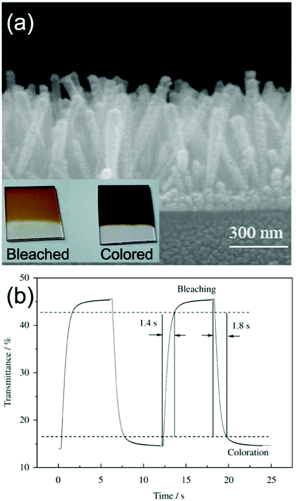
On the other hand, hydrothermal fabrication of self-supported Co3O4 (the common electrochromic cobalt oxide) 1D nanostructures is much easier. Additionally, as demonstrated in the literature reports about electrochemical energy storage applications using Co3O4 nanostructures, the better rate and cycling performance of self-supported Co3O4 1D nanostructures than many other Co3O4 nanoarchitectures indicated their superiority of highly reversible and fast redox kinetics,130,131 implying the possible achievement of satisfactory color saturation for fast switching response. Self-supported Co3O4 nanorod and nanofiber arrays can be hydrothermally grown on TCO substrates.132–135 Furthermore, by pre-preparing seeds on the substrates, uniform morphology and controlled areal density of Co3O4 nanofiber or nanorod arrays can be prepared.136,137 Xia et al. fabricated self-supported Co3O4 nanorod arrays on an ITO substrate using a seed-assisted hydrothermal process.136 The authors delicately controlled the diameter and length of the Co3O4 nanorods to optimize the electrochromic properties. The arrays of Co3O4 nanorods with diameters varying from 70 to 100 nm and a length of about 550 nm showed obvious color changes from light brown (bleached) to black (colored) with fast switching response (1.8 and 1.4 s for colored and bleached states, respectively) (Fig. 7a and b). Furthermore, this Co3O4 nanorod arrays also demonstrated quite good cycling stability with a transmittance modulation maintenance proportion of 88% after 4500 cycles. Such high satisfactory color saturation achieved in short switching time and high cycling stability was consistent with the high-rate electrochemical energy storage performance of self-supported Co3O4 1D nanostructures.130,131
 | ||
| Fig. 7 (a) SEM image of Co3O4 nanorod arrays on an ITO substrate prepared by a seed-assisted hydrothermal process. Inset digital photos demonstrate the color contrast between coloration and bleaching. (b) Transmittance modulation response of Co3O4 nanorod arrays under alternative voltages. Reprinted from ref. 136. Copyright 2010 Elsevier. | ||
Vanadium oxide and molybdenum oxide. Crystalline vanadium oxide and molybdenum oxide have been widely studied for electrochemical redox-based applications because of their attractive layered structure.138 The two-dimensional crystalline sheet structures are formed by MO6 (VO6 or MoO6) octahedra sharing corners and/or edges. Due to the layered structure, vanadium oxide and molybdenum oxide can demonstrate fast ion insertion/extraction kinetics in the interlamination of (001) planes. In addition, as typical extrinsic pseudocapacitor materials, 1D vanadium oxide and molybdenum oxide nanomaterials could exhibit enhanced pseudocapacitive effect, high Li-ion diffusion coefficient, and short characteristic relaxation process,139 which are beneficial for high optical modulation and fast switching response.
V2O5, as the common hydrothermally prepared vanadia type showing both cathodic and anodic coloration, has been widely investigated as a counter electrode material in electrochromic devices,10,139,140 because of not only its unique electrochromic performance but also its high Li-ion storage capacity. 1D V2O5 nanostructures can be facilely prepared using a hydrothermal method due to the strong preferential growth derived from the obvious lattice anisotropy of the layer crystalline structure.141–143 Chu et al. hydrothermally prepared V2O5 nanorod array films on FTO substrates and investigated their electrochromic performance (Fig. 8a).144 It was found that the V2O5 nanorod array films demonstrated obvious absorbance modulation in the visible spectrum range and vivid color changes between pale blue (cathodic coloration) and yellow-green (anodic coloration) (Fig. 8b).
 | ||
| Fig. 8 (a) SEM image of V2O5 nanorod arrays directly grown on an FTO substrate by using a hydrothermal method. (b) Optical modulation of V2O5 nanorod arrays derived from a Li-ion insertion/extraction process. Inset digital photos and plot of absorbance vs. time under alternative voltages indicate the electrochromic color contrast and switching response performance. Reprinted from ref. 144. Copyright 2016 Elsevier. | ||
Molybdenum oxide can be used as a cathodic electrochromic material with color changes between transparent and blue.10,138 MoO3 is the most common form of hydrothermally prepared molybdenum oxide. To date, self-supported MoO3 nanorod arrays have been successfully prepared using hydrothermal methods.145,146 MoO3 nanorods, nanofibers, and nanobelts powders were also hydrothermally prepared for high-performance electrochemical energy storage and electrochromism.147–149 However, research about the fabrication and investigation of self-supported MoO3 1D nanostructures on TCO substrates for electrochromism is still rare.
Doped metal oxides. Doping the metal oxides with guest ions or molecules is an effective approach to affect the coordination of host metal-oxide octahedra, generating a new electronic structure or band structure which could bring unusual electrochromic performance differing from pure host metal oxides.3,150–152 In addition, the guest ions and molecules could bring lattice distortion and defects, affecting the diffusion behaviors of inserted ions in the host metal oxides.151,153–156 Research has indicated that the widened interlamellar spacing of V2O5, MoO3 and TiO2 not only facilely accelerated the Li-ion insertion speed but also made the insertion of metal ions with larger radius (such as Na+ and K+) possible.151,154–156
A hydrothermal process is an effective and facile method to synthesize 1D uniformly doped metal oxide nanostructures, broadening the research horizon of electrochromism. For instance, the Ni-doping significantly increased the optical modulation of WO3 nanorods.157 When the Ni atomic concentration was 1.5%, the Ni-doped WO3 nanorods exhibited maximum transmittance modulation and charge density of 86.0% (at λ = 600 nm) and 24.6 mC cm−2, compared to the corresponding relatively low values of pure WO3 nanorods (50.9% and 18.2 mC cm−2, respectively). In addition, the switching response time was shortened to around 2 s. The detected increase of electrical conductivity was believed to be an important feature. Doping also can significantly enhance the optical modulation of metal oxides in the NIR and IR spectrum range. Zhou et al. reported that 2% Mo-doped WO3 nanofibers showed a high transmittance modulation in the visible and NIR spectrum range (56.7%, 83% and 48.5% at λ = 750 nm, 1600 nm and 10 μm, respectively), while the pure WO3 nanofibers only exhibited 44.4%, 52.6% and 25.1% at the three above mentioned wavelengths.158 Additionally, the enhanced electrical conductivity accelerated the switching speed to around 4 s. Nevertheless until now, the majority of these hydrothermally prepared 1D doped metal oxide nanostructures were in the powder form, and the fabrication of electrochromic 1D metal oxide nanostructures directly grown on TCO substrates for electrochromism deserves to be investigated.
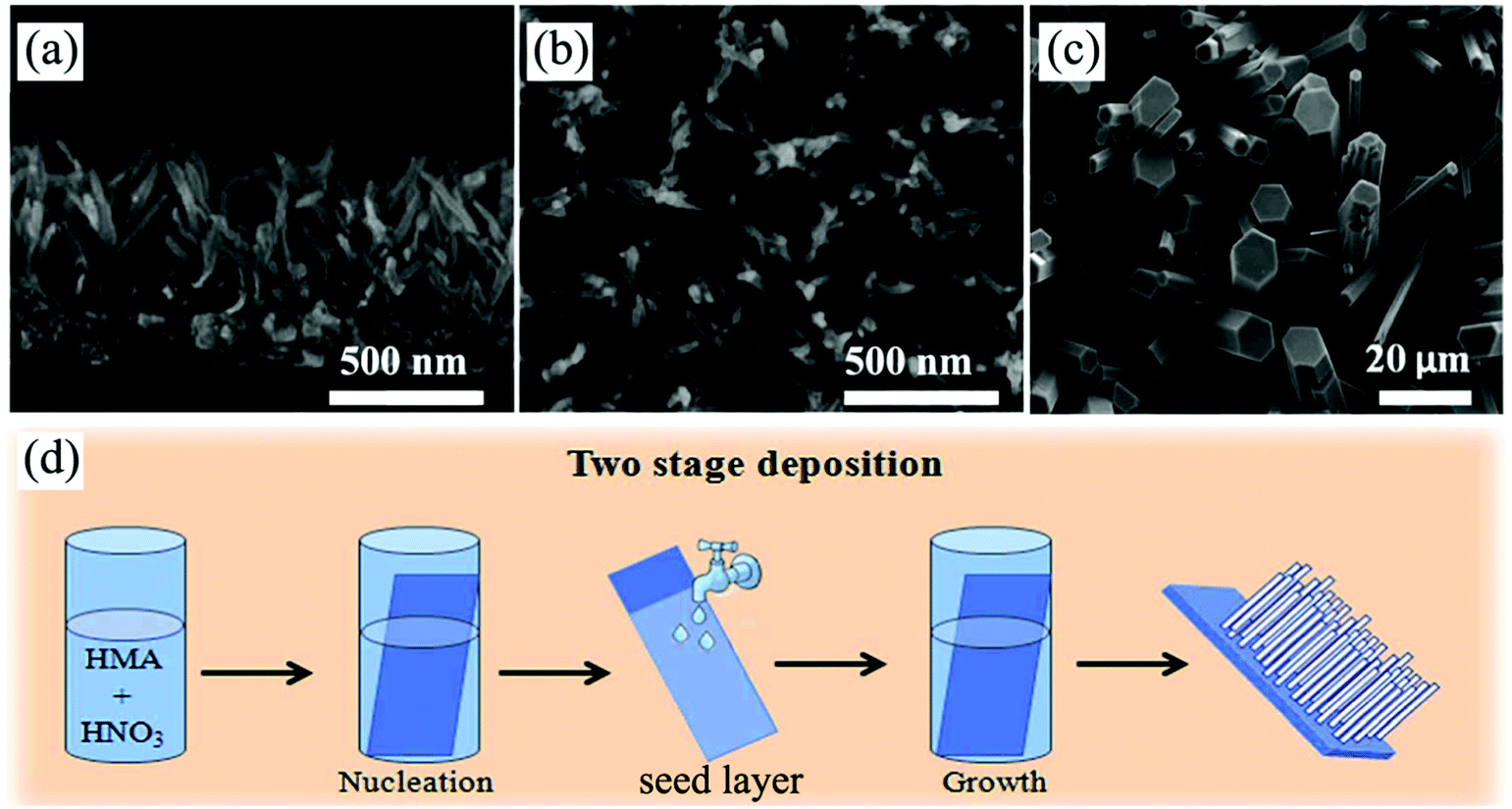 | ||
| Fig. 9 (a and b) Cross-sectional and top-view SEM images of self-supported H2Ti5O11·3H2O nanowire arrays prepared by a modified CBD method. Reprinted from ref. 167. Copyright 2014 Royal Society of Chemistry. (c and d) Top-view SEM image of MoO3 nanorod arrays and the corresponding schematic diagram illustrating the preparation process of a seed-based CBD. Reprinted from ref. 168. Copyright 2014 Royal Society of Chemistry. | ||
5.2 Vapor process-deposited self-supported 1D metal oxide nanostructures
Vapor process deposition is a direct and bottom up method to prepare self-supported 1D metal oxide nanostructures on substrates.169 Because the metal oxide nanostructures are grown from gaseous precursors, solid substrates are needed to provide low energy sites for nucleation and subsequent crystal growth. In a vapor deposition process, thermal activation under high temperature is usually employed to facilitate crystal nucleation and growth on the TCO substrate. The high experimental temperature makes the as-prepared self-supported 1D metal oxide nanostructures fully crystallized, even in single-crystal nature. Similar to a crystal growth mechanism under hydrothermal conditions, the production of 1D crystalline metal oxide nanostructures on TCO substrates is naturally formed due to the preferential direction of the anisotropic crystal lattice with or without external physical forces. In addition, employing catalysts or surface modification on substrates can affect the nucleation and crystal growth processes, controlling the morphology or phase of the produced self-supported 1D metal oxide nanostructures.170,171 Typically, vapor process deposition can be categorized into physical and chemical vapor deposition (PVD and CVD) processes.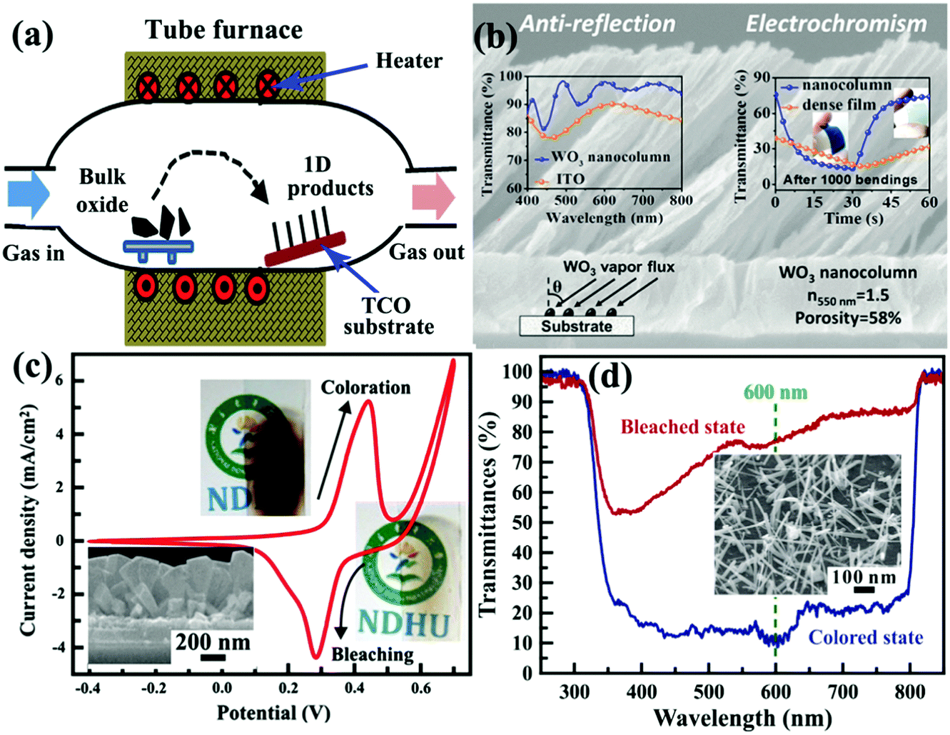 | ||
| Fig. 10 (a) Schematic diagram of tube furnace for synthesis of self-supported 1D metal oxide nanostructures by a PVD process. (b) Cross-sectional SEM image of three-dimensional, high-porous, and oriented WO3 nanocolumn layer prepared by a glancing angle PVD method. Left inset figure demonstrates the optical transmittance spectrum of bare ITO and ITO/WO3 films at normal incidence. Right inset figure demonstrates the transmittance modulation switching response curves of dense and three-dimensionally porous PET/ITO/WO3 films. Reprinted from ref. 178. Copyright 2016 American Chemical Society. (c) Electrochemical and electrochromic performance of self-supported NiO nanorods prepared by the HFMOVD method. Inset figure is the SEM image of the NiO sample. Reprinted from ref. 184. Copyright 2013 Elsevier. (d) Transmittance modulation of self-supported brookite TiO2 nanoneedles prepared by the HFMOVD method. Inset figure is the SEM image of the TiO2 sample. Reprinted from ref. 185. Copyright 2015 Elsevier. | ||
Aerosol-assisted chemical vapor deposition (AACVD) is another widely used CVD process employing metal-containing compounds as sources to prepare self-supported 1D metal oxide nanostructures for high electrochromism. In AACVD, metal-containing reactants are transported in solution as a mist, and therefore, compound volatility is less critical than in conventional CVD, which has an important influence on the morphology of the products.186 Various electrochromic self-supported 1D metal oxide nanostructures, such as NiO nanorod arrays,186 WO3 nanoneedle arrays187 and WO3 nanorod arrays,188 were prepared using AACVD on TCO substrates.
5.3 Anodic oxidation prepared self-supported metal oxide nanotube arrays
Fabrication of metal oxide nanotube arrays by anodic oxidation on metal foils has received enormous interest due to the wide applications of metal oxide nanotube arrays in the fields of energy storage and conversion, sensors, and biomedical applications.189 The anodic formation mechanism of metal oxide nanotubes on the clean surface of metal foil in an electrolyte has been previously detailed.189 Typically, once a sufficient potential is applied, the metal atoms (M) on the surface are oxidized into metal ions (Mn+) while the O2− are generated by deprotonation of water in the electrolyte, producing a thin barrier metal oxide (MOx) layer on the foil surface. Field-assisted dissolution of the metal oxide occurs at the oxide/electrolyte interface as the M–O bonds undergo polarization and are weakened. In the presence of some active ions (such as F−) which can react with Mn+ forming water-soluble complexes, small pits in the oxide layer form. In the pits, O2− ions continue to diffuse through the oxide layer and then react with the metal to produce fresh metal oxide at the bottom. When the rate of oxide growth at the metal/metal oxide interface and the rate of oxide dissolution at the metal oxide/electrolyte interface ultimately become equal, amorphous nanowalls between the pits are formed. The metal oxide growth/dissolution process moves further into the metal making the pore deeper, finally generating nanotube arrays on the foil. An annealing treatment is needed to make the amorphous products fully crystallized (Fig. 11a). Furthermore, anodic oxidation of alloy foils is a facile way to prepare doped (or mixed) metal oxide nanotube arrays, which can exhibit unusual electrochemical kinetics and/or new electrochromism.189,190 Mott–Schottky analysis indicated that the doped crystalline metal oxide nanotube arrays demonstrated higher electrical conductivity than the pure crystalline metal oxide nanotube arrays.190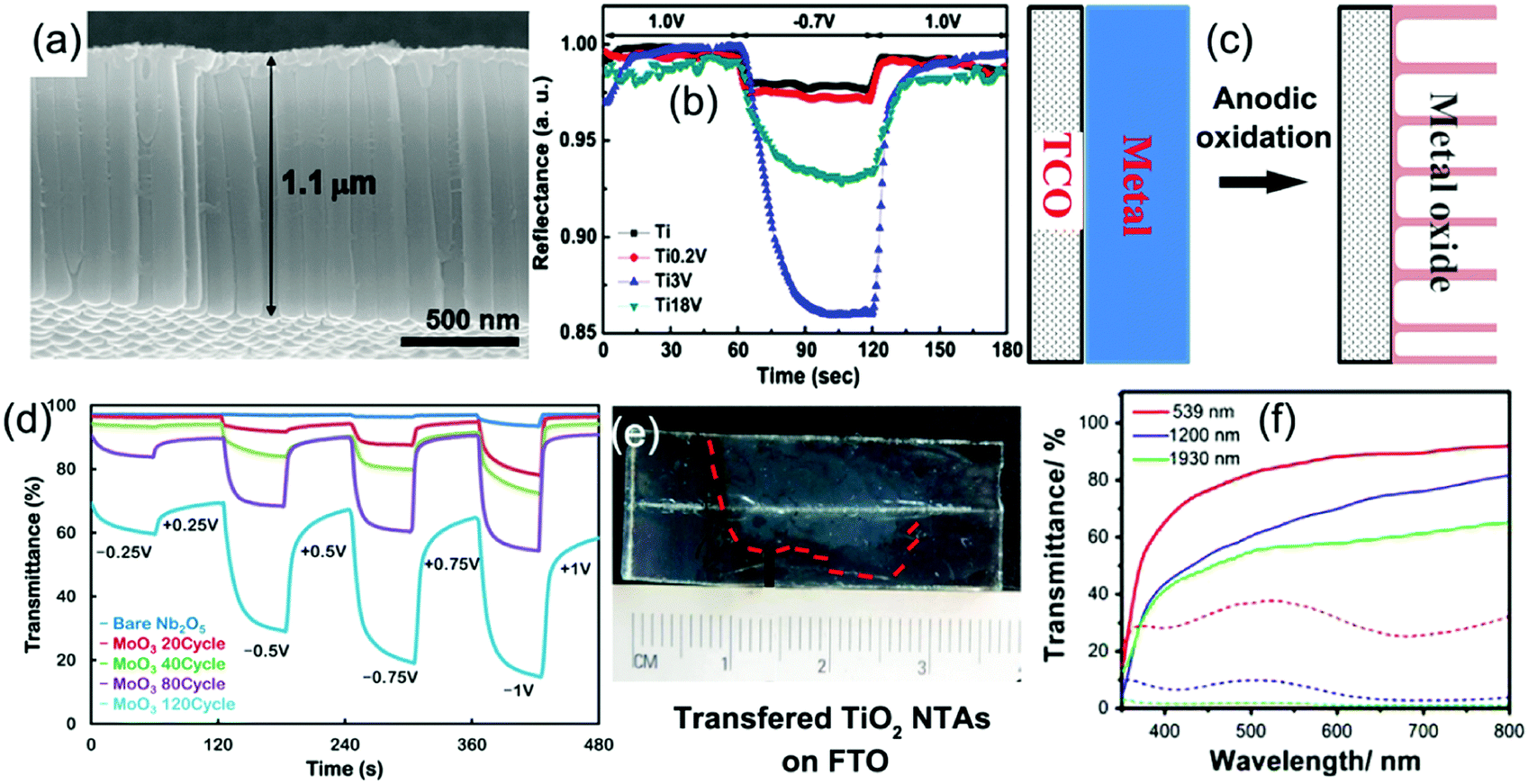 | ||
| Fig. 11 (a) Typical SEM image of anodic TiO2 nanotube arrays. (b) Reflectance modulation curves of mixed Ti–V–O nanotube arrays with different vanadium atom concentrations. Reprinted from ref. 196. Copyright 2011 Elsevier. (c) Schematic diagram illustrating preparation of anodic metal oxide nanotube arrays directly grown on TCO substrates. (d) The influence of coated amount of MoO3 on the transmittance modulation of anodized Nb2O5/electrodeposited α-MoO3 binary films. Reprinted from ref. 208. Copyright 2014 American Chemical Society. (e and f) Digital photos of free anodic TiO2 nanotube arrays transferred on the FTO substrate and their transmittance modulation performance. Reprinted from ref. 213. Copyright 2016 Elsevier. | ||
The initial electrochromic applications of anodic metal oxide nanotube arrays were in reflectance-mode because of the difficulty in peeling off the nanotube arrays from the metal substrate.191–198 For instance, H+ insertion/extraction led to a reversible reflectance modulation of over 50% and a fast switching response of 2 s at λ = 480 nm in the TiO2 nanotube arrays (film thickness of 1 ± 0.1 μm with an individual tube diameter of 100 ± 10 nm and a tube wall thickness of 10 ± 2 nm),191 while Li+ insertion/extraction could result in a reflectance modulation of approximately 35% at the same wavelength with a switching time of 5 s.192 CV measurements indicated that the TiO2 nanotube arrays showed improved H+ and Li+ chemical diffusion coefficients. Yang et al. reported that the V2O5 nanotube arrays with a length of 20 μm and pore diameter of 12 nm could demonstrate a reflectance modulation of over 30% with vivid color change from yellow to green and then dark accompanied by an increased amount of inserted Li-ions.193 In addition, the as-prepared V2O5 nanotube arrays also exhibited high cycling stability with negligible degradation of reflectance contrast after 250 cycles.
Anodic oxidation of alloy foils produced doped metal oxide (or mixed metal oxides) nanotube arrays. Ghicov et al. synthesized tungsten-doped titanium oxide nanotube arrays using Ti–W alloys.194 It was found that the doped products exhibited higher reflectance modulation and charge density than the pure TiO2 nanotube arrays. Ghicov et al. also found that the Ti–Nb–O nanotube arrays anodically prepared from β-Ti45Nb alloy exhibited a pure phase of anatase TiO2, while the lattice interlamellar spacing was widened due to the Nb-doping.195 Such widened lattice interlamellar spacing facilitated the Li+ insertion/extraction process, leading to increased reflectance modulation of approximately 80% at λ = 600 nm and high charge density of 126.1 mC cm−1, compared to the corresponding values of approximately 50% and 76.4 mC cm−1 for pure TiO2 nanotube arrays. Yang et al. anodically synthesized mixed TiO2–V2O5 nanotube arrays from Ti–V alloys.196 Maximum values of reflectance modulation and charge density were achieved for the nanotube arrays prepared from a Ti–V alloy with 3 at% vanadium during the Li-ion insertion/extraction process (Fig. 11b). In addition, the doping of vanadium also significantly enhanced the color contrast by increasing color saturation under cathodic polarization. Anodically prepared mixed Ti–Mo–O and W–Ta–O nanotube arrays also demonstrated enhanced reflectance modulation performance.197,198 In addition, the nanotube arrays provided large surface area for decoration of a second type of electrochromic material, such as silver phosphate crystals199 and WO3 nanocrystals,200 resulting in enhanced reflectance modulation and multicolor changes. Furthermore, mesoporous NiO201 and WO3202 films were also prepared by anodic oxidation processes for reflectance-mode electrochromic electrodes.
Anodic oxidation of metal layers deposited on the TCO substrates is an easy approach to directly prepare nanotube array electrodes for transmittance-mode electrochromic devices (Fig. 11c). The typical process to deposit metal layers was magnetron sputtering, and meanwhile heat-stable TCOs, such as ITO and FTO, were used as substrates.203,204 Barredo-Damas et al. prepared anodic Nb2O5 nanotube arrays with a thickness of 1 μm from a thin Nb-layer on FTO glass.205 The as-prepared nanotube arrays exhibited a high transmittance modulation of ca. 90% at λ = 600 nm with obvious color changes in 0.1 M HClO4. Yao et al. synthesized self-supported TiO2 nanotube arrays for electrochromic applications by anodic oxidation of an RF sputtered titanium layer on an FTO substrate.206 To further increase the optical modulation, α-MoO3 of ∼5 to 15 nm thickness was electrodeposited on the wall surfaces of the TiO2 nanotube arrays. The MoO3/TiO2 system showed a 4-fold increase in optical density over bare TiO2 when the thickness of the MoO3 coating was optimized. The enhancement was ascribed to (I) the desirable electron band coupling effect between α-MoO3 and TiO2 for feasible charge carrier transfer, (II) the increased amount of inserted Li-ions derived from the layered structure of α-MoO3 and (III) enhanced electron transport derived from the high electrical conductivity of α-MoO3 layers acting as efficient pathways for charge carrier transfer.206,207 Yao et al. also synthesized anodized Nb2O5/electrodeposited α-MoO3 binary films for high electrochromism.208,209 The thickness of the MoO3 layer was controlled by different electrodeposition cycles (a cycle was a chronoamperometric deposition of 60 s). It was found that the increased thickness of the MoO3 layer led to an increase of transmittance modulation, reaching a favorable value of approximately 45% at λ = 550 nm between ±1 V in a 0.1 M LiClO4/PC electrolyte (Fig. 11d). WO3 mesoporous film electrodes were prepared by anodic oxidation treatment on the corresponding metal layers deposited on FTO substrates.210 These films also exhibited high transmittance modulation with fast switching response.
Free TiO2 nanotube array membranes can be peeled off from the Ti substrates using a modified anodic oxidation process.211,212 Transfer of these membranes on TCO substrates also achieves transmittance-mode electrochromic electrodes. Lv et al. developed a two-step anodization process to prepare free TiO2 nanotube array membranes with various thicknesses of 539, 1200 and 1930 nm, and attached them on FTO substrates for electrochromic tests (Fig. 11e).213 It was found that the thickness had a strong effect on the transmittance modulation in the whole visible spectrum range (Fig. 11f). Typically, the 539 nm-thick TiO2 nanotube array membrane exhibited a transmittance modulation of 65% at λ = 750 nm. In addition, the TiO2 membrane also exhibited high cycling stability with a high maintained transmittance modulation of 57% and a negligible degradation of coloration efficiency after 1000 cycles. Furthermore, decoration of WO3 nanocrystals on the surface of TiO2 nanotube arrays further increased the transmittance modulation and color contrast between coloration and bleaching states.214
5.4 Other processes for self-supported metal oxide 1D nanostructures
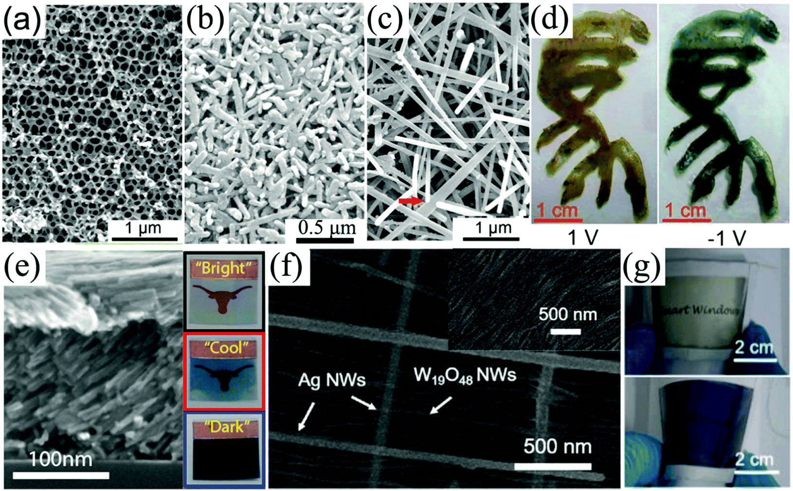 | ||
| Fig. 12 (a) SEM image of 3D macroporous amorphous vanadium oxide films prepared by electrodeposition with the assistance of polystyrene colloidal crystals as templates. (b and c) SEM images of V2O5 nanorods and nanofiber grassland prepared by annealing treatment on 3D macroporous amorphous vanadium oxide films. Reprinted from ref. 218. Copyright 2015 Wiley. Reprinted from ref. 220. Copyright 2015 Macmillan Publishers Limited. (d) Electrochromic performance of the V2O5 nanofiber grassland. (e) Cross-sectional SEM image of a flexible WOx–NbOx composite film electrode. Inset digital photos demonstrate the three-stage transmittance modulation in the visible and NIR regions. Reprinted from ref. 232. Copyright 2017 American Chemical Society. (f and g) SEM image and electrochromic performance of coassembled Ag/W18O49 nanofiber networks on the PET substrate. Reprinted from ref. 239. Copyright 2017 American Chemical Society. | ||
Self-supported nanorod arrays of other electrochromic metal oxides, including Co3O4,226 NiO227 and WO3228 have also been prepared by annealing treatment on the corresponding amorphous films, while the morphology and phase transformation mechanisms are still not clear.
Yoo et al. solvothermally prepared 1D W18O49 nanobundles formed by parallelly stacking tens of W18O49 nanowires in the diameter direction.235 Then a series of nanobundle-assembled porous films on ITO substrates were prepared by LB technology under different maximum surface pressures. A superior transmittance of ca. 33% at λ = 633 nm with a coloration efficiency of 47.5 cm2 C−1 was achieved when the proper maximum surface pressure was used. Wang et al. assembled the hydrothermally prepared WO3 nanorods (diameters of ∼100 nm and lengths of ∼2 μm) into a film on ITO substrates using an LB process.237 The as-assembled WO3 film exhibited multicolor changes (green, green-blue, and blue), high transmittance modulation of ∼ 66% at λ = 632.8 nm, and high intercalated charge of ∼133 mC cm−2 mg−1 compared to many other WO3 nanostructured films. The authors also found that the assembly was not affected by the surface properties of the substrates, but was dependent on the drying rate of the film, the concentration of the suspension, and the aspect ratio of the nanorods. Liu et al. found that the use of a surfactant was the key factor to effectively assemble metal oxide nanofibers with high length-to-diameter ratios.238 By using LB assembly with W18O49 nanofibers (sub 5 nm in diameter and tens of micrometers in length) and poly(vinyl pyrrolidone) (PVP), the authors achieved high electrochromic films on ITO substrates. Interestingly, W18O49 nanowires and Ag nanowires can be co-assembled as hybrid networks on PET substrates by an LB process, creating ITO-free flexible electrochromic electrodes (Fig. 12f).239 The mAg:mW18O49 mass ratio was 14:4. The hybrid film with optimized thickness exhibited high conductivity (7 Ω per square), high transmittance modulation of 68% at λ = 632.5 nm, fast switching response (3.92 and 7.78 s for coloration and bleaching, respectively) and good bending strength stability (Fig. 12g).
5.5 Solution process-deposited self-supported 1D conductive polymer nanostructures
Chemical oxidative and electrochemical polymerizations are the two most general methods used for synthesizing self-supported 1D conductive polymer nanostructures from solutions containing monomers. The generation of conductive polymer 1D nanostructures during the polymerization process seems to have a strong relationship with the intrinsic polymerization mechanism.240 For the typical conductive polymer of PANI, it was found that the polymerization of aniline monomers on substrates covered two different stages.241,242 In the first stage, a compact PANI layer was formed on the substrate because of the 2D nucleation manner. While in the second stage, the nucleation changed to a 1D manner, producing branched PANI nanostructures (i.e. 1D nanostructures) due to autocatalytic oxidation of aniline on PANI formed in the first stage. In some cases, surfactants were added into the monomer-containing solutions to facilitate the production of PANI 1D nanostructures when the surfactant concentration was higher than the value of the critical micelle concentration.2431D conductive polymer nanostructures were much easier to be synthesized when chemical oxidative polymerization occurred under low temperature such as from 0 to 5 °C.244,245 Zhang et al. prepared randomly stacked PANI nanotubes about 80–180 nm in diameter in the presence of D-10-camphorsulfonic acid as the dopant under ice bath conditions.244 Vertically aligned PANI nanowires with ∼50 nm average diameter and ∼600 nm length were synthesized by Wang et al. using a similar polymerization process.245 Chiou et al. developed a novel dilute polymerization method to produce a large quantity of interconnected and networked PANI nanofibers in bulk solutions on various substrates, including conducting and non-conducting substrates.246–248 In a typical dilute polymerization process, substantially lower concentrations of aniline and oxidant than the usually employed values were used. The diameters of the tips of the nanofibers can be controlled within the range of 10–40 nm, and the average length can be controlled within the range of 70–360 nm (Fig. 13a).248 These PANI nanofiber arrays grown on TCO substrates exhibited high redox kinetics, leading them to be desirable for bi-functional electrochromic energy storage applications, as shown in the following part about electrochromism-containing multifunctional devices.
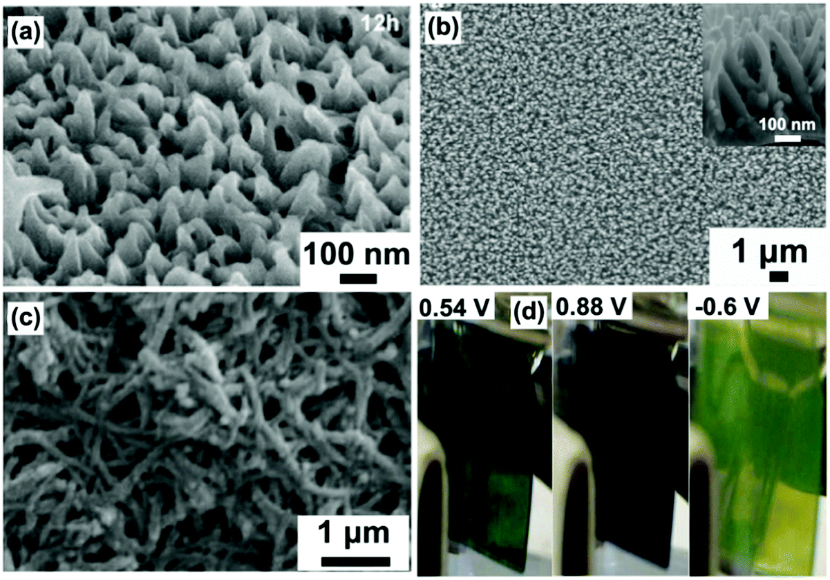 | ||
| Fig. 13 (a) SEM image of PANI nanofiber arrays prepared by using a dilute polymerization method. Reprinted from ref. 248. Copyright 2018 Elsevier. (b) SEM image of PPy nanofiber arrays electropolymerized by a galvanostatic method. Reprinted from ref. 253. Copyright 2016 Elsevier. (c and d) SEM image and electrochromic color changes of a PANI/inorganic salt binary nanofiber network. Reprinted from ref. 255. Copyright 2016 Springer. | ||
Galvanostatic, potentiostatic, and cyclic voltammetry methods are three common technologies for electropolymerization of conductive polymers.249–251 The morphologies of electropolymerized nanostructures varied a lot from the used techniques. Due to the ease of 1D nucleation, a galvanostatic method was widely used to prepare vertically aligned conductive polymer 1D nanostructures, such as PANI and PPy nanorod and/or nanowire arrays on various conductive substrates.251–253 The morphology characters, such as areal density, length and diameter of 1D active materials can be easily controlled by varying the experimental parameters such as electropolymerization current densities and times. Fig. 13b showed a typical SEM image of PPy nanofiber arrays prepared using galvanostatic electropolymerization.253 By simply changing the electropolymerization time, the length of the PPy nanofibers varied from 1.5 to 4 μm accompanying the increase of diameter from 80 to 100 nm.252,253 When the conductive polymers were polymerized using potentiostatic, and cyclic voltammetry methods, the products usually exhibited a porous nanofiber network morphology built by random twisting of nanofibers.250,254–256Fig. 13c demonstrates a typical SEM image of a PANI/inorganic salt (LiClO4) binary nanofiber (diameter of 80–110 nm) network electropolymerized at a constant potential of 0.9 V versus Ag/AgCl.255 This nanofiber network exhibited three-color changes and high transmittance modulation in the visible spectrum range with a maximum value of ca. 50% at λ = 560 nm (Fig. 13d). Osuna et al. prepared a PEDOT nanofiber network on a flexible transparent single-wall carbon nanotube/PET electrode.256 This flexible electrochromic electrode showed a high transmittance modulation of ca. 38% at λ = 550 nm, fast switching response time (2.4 and 1.1 s for coloration and bleaching, respectively), and high cycling stability with negligible performance degradation after 1000 cycles.
6. Core/shell 1D nanostructures for electrochromism
6.1 Inorganic/inorganic core/shell 1D nanostructures
Her et al. synthesized crystalline/amorphous WO3 core/shell nanorod powders using a two-step hydrothermal process and then fabricated a porous film by the drop assembly method.26 Compared to pure nanorod and amorphous films, the crystalline/amorphous WO3 core/shell nanorods assembled film exhibited increased transmittance modulation of 44% at λ = 550 nm with acceptable switching response (41 and 6 s for coloration and bleaching respectively). Crystalline/amorphous WO3 core/shell nanorod arrays directly grown on FTO substrates exhibited better electrochromic performance than the film fabricated by drop assembly.261 Because of efficient electron transport as well as the enhanced synergistic effect between the amorphous shells and crystalline cores, the nanorod array electrode showed improved optical modulation both in the visible and IR regions (70.3% at λ = 750 nm, 42.0% at λ = 2000 nm and 51.4% at λ = 10 μm), fast switching speed (3.5 and 4.8 s for coloration and bleaching, respectively), and excellent cycling performance (maintained transmittance modulation of 68.5% after 3000 cycles). Self-supported core/shell nanorod arrays of crystalline/amorphous TiO2 on FTO substrates fabricated by hydrothermal then layer-by-layer methods were demonstrated by Chen et al. (Fig. 14a).262 The layer-by-layer method was beneficial to produce uniform and thin amorphous shells as well as high-quality chemical and physical contacts at the phase interfaces (Fig. 14b). The arrays of crystalline/amorphous TiO2 core/shell nanorods with an optimal amorphous layer thickness of 13 nm possessed notably larger optical contrast (43%) and higher coloration efficiency (16.2 cm2 C−1) than crystalline TiO2 nanorod arrays (18%, 8.8 cm2 C−1) at λ = 800 nm. In addition, it was interesting and meaningful to note that the coating of an amorphous shell significantly enhanced the redox stability of crystalline TiO2 nanorods in a larger potential window.
 | ||
| Fig. 14 (a) Schematic diagram illustrating preparation of self-supported crystalline/amorphous TiO2 core/shell nanorod arrays. (b) HRTEM image of a crystalline/amorphous TiO2 core/shell nanorod. Reprinted from ref. 262. Copyright 2017 Elsevier. (c and d) Cross-sectional SEM images of TiO2 nanorod arrays and TiO2/Prussian blue core/shell (TiO2@PB) nanorod arrays. (e) In situ transmittance response at λ = 700 nm of the PB-based and TiO2@PB-based electrochromic devices (ECDs). Reprinted from ref. 280. Copyright 2017 Elsevier. | ||
Based on whether the oxides of the cores are electrochromic or not, M1Ox/M2Oy core/shell 1D nanostructures can be separated into two categories. In the first category, the 1D M1Ox oxide cores act as strong mechanical and highly conductive skeletons to deposit M2Ox shells with large surface area and efficient redox reactions. To obtain high color contrast in the M2Ox shells, the 1D M1Ox skeletons are expected to demonstrate high transparency and negligible redox reactions when the M2Ox shells show electrochromism. Thus, 1D ZnO and SnO2 nanostructures are ideal skeletons. Wang et al. presented a flexible electrochromic display electrode based on amorphous WO3 nanoparticle-modified ZnO nanorod arrays on ITO/PET substrates prepared by using a facile hydrothermal process and pulsed laser deposition (PLD) method.264 The as-prepared ZnO/WO3 core/shell nanorod arrays exhibited faster switching response time of ca. 5 s for both coloration and bleaching with higher coloration efficiency than many WO3 nanorod arrays. Bi et al. investigated the influence of WO3 shell thickness and morphology on the electrochromic performance of ZnO/WO3 core/shell nanorod arrays prepared on AZO/PET substrates employing a similar synthesis method.265 By using an optimized thickness and morphology of the WO3 shells, the ZnO/WO3 core/shell nanorod arrays exhibited a high transmittance modulation of 68.2% at λ = 633 nm and a large coloration efficiency of 80.6 cm2 C−1 with unusual color changes between transparent and black, compared to transparent/blue changes for pure WO3 nanostructures. Zhang et al. prepared hierarchical SnO2/NiO core/shell nanostructures on FTO substrates by a two-step hydrothermal process.266 Compared to the pure NiO nanostructures, the SnO2/NiO core/shell nanostructures exhibited higher transmittance modulation in the whole visible spectrum range, better cycling stability and a notably better memory effect under open-circuit conditions due to the enhancements of charge storage in NiO derived from the electron band structure and high electrical conductivity of SnO2 cores.
As for the second category where M1Ox and M2Oy are two electrochromic oxides, the M1Ox/M2Oy core/shell 1D nanostructures could demonstrate enhanced and/or new electrochromic performance compared to the pure M1Ox and M2Oy nanoelectrodes. Until now, NiO/V2O5,267 WO3/TiO2,53,268,269 TiO2/NiO,270,271 TiO2/WO3,272,273 lithium-titanate/WO3,274 TiO2/V2O5,275 and TiO2/MoO3276 core/shell 1D nanostructures have been fabricated for electrochromic applications. The electrochromic performance of these M1Ox/M2Oy core/shell 1D nanostructures was highly dependent on the mass ratio of the two oxides. For example, as shown in Table 1, TiO2/WO3 core/shell nanorod arrays prepared by a two-step approach including hydrothermal and electrodeposition processes exhibited better performance than pure WO3 films and TiO2 nanorod arrays. Their transmittance modulation and switching response time varied a lot when the thickness of the WO3 shell changed.272 The M1Ox/M2Oy core/shell 1D nanostructures could also exhibit better cycling stability and higher coloration efficiency than the pure M1Ox and M2Oy nanostructures as demonstrated in the electrochromic performance of WO3/TiO2,53,269 TiO2/NiO,270 TiO2/WO3,272 and TiO2/V2O5275 core/shell nanorod arrays. Electrochemical analysis indicated that the enhanced redox kinetics including the improved Li+ diffusion coefficient and efficient interfacial electron transport were important features.
| Sample | Transmittance modulation (%) | Switching time (s) | |||
|---|---|---|---|---|---|
| λ = 700 nm | λ = 1800 nm | λ = 10 μm | Coloration | Bleaching | |
| Pure WO3 | 31.6 | 35.5 | 6.9 | 5.0 | 5.2 |
| Pure TiO2 | 4.3 | 3.1 | 0.6 | 0.6 | 3.6 |
| TiO2@200WO3 | 40.3 | 70.3 | 38.4 | 2.4 | 4.4 |
| TiO2@400WO3 | 52.2 | 46.3 | 37.2 | 3.2 | 4.6 |
| TiO2@600WO3 | 57.2 | 38.2 | 17.8 | 6.4 | 5.4 |
Polyoxometalates are a newly emerging class of transition metal-containing nanoclusters with intriguing structures and diverse redox properties for electrochromism.281,282 Coating polyoxometalates on metal oxide 1D nanostructures can significantly enlarge their surface area and shorten the ion diffusion distance, resulting in enhanced electrochromic performance. Liu et al. synthesized Dawson-type polyoxometalate K6P2W18O62@TiO2 hybrid nanowire arrays on FTO substrates by combining hydrothermal and layer-by-layer assembly methods.283 The as-prepared hybrid nanowire arrays exhibited higher transmittance modulation (45.1% at λ = 650 nm) and faster switching times (1.9 and 6.7 s for coloration and bleaching, respectively) than the K6P2W18O62 dense film (corresponding values of 31.2%, 5.3 s and 10.5 s, respectively).
6.2 Inorganic/organic core/shell 1D nanostructures
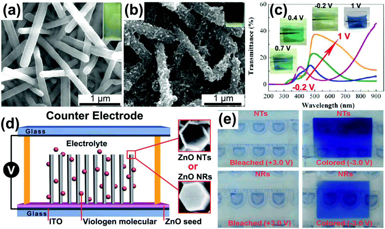 | ||
| Fig. 15 (a and b) SEM images of coaxial and branched V2O5/PANI core shell nanorod arrays, respectively. The color of the samples indicates the different loaded mass of PANI shells. Reprinted from ref. 287. Copyright 2017 Elsevier. (c) Transmittance modulation of TiO2/PANI core shell nanorod arrays under different voltages in 0.1 M HCl solution. Inset digital photos indicate the color changes under different voltages. Reprinted from ref. 286. Copyright 2013 American Chemical Society. (d and e) Schematic and electrochromic color contrast of electrochromic devices with viologen-modified ZnO NT (or NR) arrays as the working electrode. Reprinted from ref. 299. Copyright 2016 Royal Society of Chemistry. | ||
Various electrochromic metal oxide/conductive polymer core/shell 1D nanostructures including NiO/PANI (or PEDOT),286,288 Co3O4/PANI (or PEDOT),286 TiO2/PANI (or PEDOT),286,289,290 WO3/PANI (or PEDOT),291–293 ZnO/PEDOT (or poly(3-methylthiophene) (PMeT)),294,295 and MoO3/PANI296 have been fabricated for electrochromism. When the metal oxide 1D cores only acted as skeletons, the conductive polymer coating layers (i.e. shells) exhibited enlarged surface area and shortened ion diffusion distance, leading to enhanced electrochromism. For instance, the TiO2/PANI core/shell nanorod arrays showed similar but enhanced electrochemical/elecrochromic performance to pure PANI films in a 0.1 M HCl aqueous electrolyte.12,286 The as-prepared hybrid nanorod arrays exhibited high transmittance modulation in the whole visible spectrum range, four distinct color changes, fast switching speeds (1.3 and 1.2 s for coloration and bleaching, respectively), and ultra-high cycling stability (Fig. 15c). Using metal oxides with higher electrical conductivity such as ZnO and SnO2 nanorod arrays, the metal oxide/conductive polymer core/shell 1D nanostructures can exhibit much enhanced electrochromic performance. Kateb et al. prepared a ZnO/PEDOT core/shell nanorod array film as an electrochromic electrode.294 This electrode showed an almost homogeneous transmittance modulation of ca. 48% in the whole visible spectrum range, ultrafast switching response time of <2.2 ms to achieve 100% transmittance saturation modulation (faster than PEDOT nanotube arrays of 50 and 70 ms for bleaching and coloration, respectively68), and ultrahigh cycling stability with no transmittance modulation degradation after 100000 cycles. Electrochemical analysis indicated that the ZnO/PEDOT core/shell nanorods exhibited a significantly improved Li+ diffusion coefficient of 2.01 × 10⁻⁴ cm2 s−1 which was 4 orders of the value of the PEDOT dense film.
When both metal oxide cores and conductive polymer shells demonstrate electrochromism, the hybrid core/shell 1D structures can exhibit unusual optical modulation characteristics. For instance, the WO3/PANI nanorod arrays exhibited color changes differing from the pure WO3 and PANI electrodes.291 The PANI showed three colored redox states under positive voltages and a light yellow or transparent state under negative voltages,250 while the WO3 presented a transparent state under positive voltages and deep blue state under negative voltages.86 This meant that the WO3/PANI nanorod arrays had a complementary dual-electrochromic effect to each other, giving rise to a new coloration phenomenon, i.e. deep blue color under both positive and negative voltages while bleaching under voltages around 0 V accompanying unique transmittance modulation characters.291 Similar electrochromic phenomena were also found in the NiO/PANI288 and MoO3/PANI296 core/shell nanostructures.
ZnO nanorod or nanofiber arrays are desirable skeletons due to their large surface area, high transparency, high electrical conductivity, electrochemical stability in the electrochromic voltage window of viologens, and easy fabrication. Sun et al. assembled an electrochromic device (ECD) using viologen-modified ZnO nanowire arrays on FTO glass as the electrochromic electrode and TiO2 nanoparticles on FTO glass as the counter electrode.297 The as-assembled ECD demonstrated obvious transparent/blue color changes, fast switching time (170 and 142 ms for coloration and bleaching respectively) and desirable cycling stability. Hu et al. fabricated a flexible viologen-based electrochromic electrode using ZnO nanowire arrays on an ITO/PET substrate as a skeleton.298 Li et al. made a comparative study of the electrochromic performance of methyl-viologen modified ZnO nanotube (NT) and nanorod (NR) arrays (Fig. 15d).299 Due to the larger surface area of the NTs than that of the NRs, the electrochromic device based on ZnO NTs exhibited higher transmittance modulation of 70% at λ = 608 nm, higher coloration efficiency of 93.5 cm2 C−1, faster switching response (6 and 3 s for coloration and bleaching, respectively), and better coloration/bleaching color contrast than the electrochromic device based on ZnO NRs (Fig. 15e).
7. 1D nanostructures for bifunctional electrochromism-involving applications
Electrochromic energy storage devices
Given that the electrochemical energy storage of metal oxides, conductive polymers, and hexacyanoferrates is also derived from the redox process, research on the integration and applications of electrochromic energy storage are becoming more and more popular.28,29,300 Many electrochromic materials, including PANI, PEDOT, TiO2, WO3, NiO, V2O5, MnO2, Prussian blue, and some hybrids have been used to fabricate electrochromic energy storage electrodes and devices.28,29,300 In addition, fabrication of self-supported 1D nanostructures could significantly enhance redox kinetics due to the electrochemical and structural advantages.8,17,252Wang et al. fabricated a symmetric electrochromic supercapacitor using PANI nanowire arrays (prepared by dilute polymerization method) on flexible PEDOT:PSS/PET substrates with gel electrolyte (Fig. 16a and b).301 In the voltage range from 0 to 1 V, the as-assembled device exhibited light yellow green (0 V)/dark blue (1 V) color changes with high areal capacitance rate performance (0.017 and 0.004 F cm−2 at scan rate of 5 and 100 mV s−1 under CV examination) (Fig. 16c).
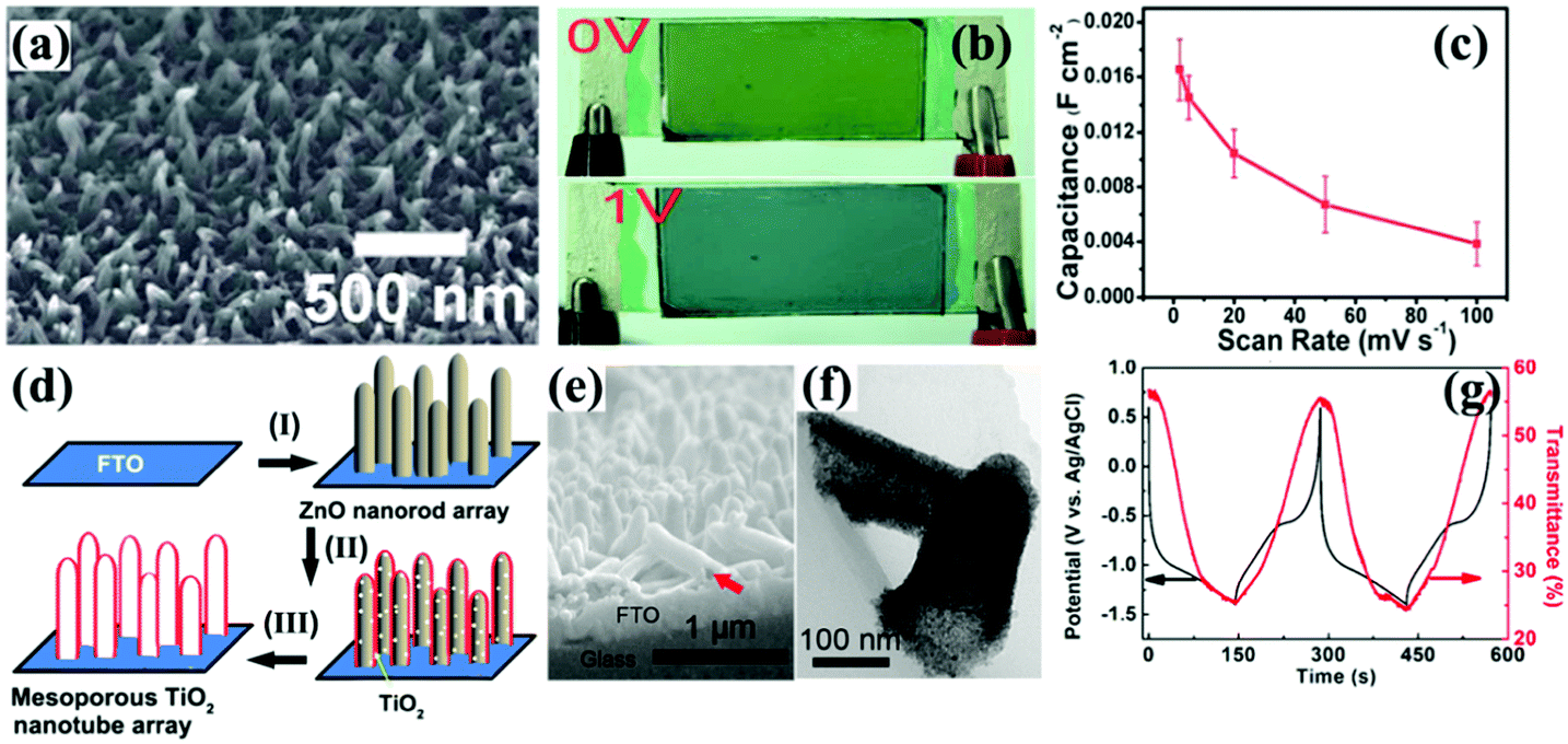 | ||
| Fig. 16 (a) SEM images of PANI nanowire arrays on a flexible PEDOT:PSS/PET substrate. (b and c) Electrochromic color contrast and energy storage performance of a symmetrical electrochromic supercapacitor using PANI nanowire arrays as electroactive materials and polymer gel as an electrolyte. Reprinted from ref. 301. Copyright 2012 Royal Society of Chemistry. (d) Schematic diagram illustrating preparation of mesoporous TiO2 nanotube arrays using STAH process. Step I was electrodeposition of ZnO nanorod arrays. Step II was immersion of ZnO into STAH solution. Step III was preparation of TiO2 mesoporous nanotube arrays by STAH and annealing treatment. (e and f) SEM and TEM images of mesoporous TiO2 nanotube arrays. (g) Transmittance modulation during the charge/discharge process of the TiO2 nanotube array electrode at a current density of 15C. Reprinted from ref. 302. Copyright 2018 Royal Society of Chemistry. | ||
As for the application of metal oxides for electrochromic energy storage, the relatively slow redox kinetics derived from low electrical conductivity and extrinsic pseudocapacitive character could seriously restrict the electrode to simultaneously deliver high desirable energy density accompanying high and fast optical modulation.139 Fabrication of 1D metal oxides in a scale of several nanometers with plenty of pores is a promising strategy. Sacrificial template-accelerated hydrolysis (STAH) using ZnO nanorod arrays as templates to prepare mesoporous metal oxide nanotube arrays stacked by several nanometer-sized oxide crystals is an ideal strategy to synthesize electrochromic energy storage electrodes with high energy and power densities.54–56 For instance, an electrodeposited ZnO nanorod arrays on an FTO substrate was used to fabricate TiO2 nanotube arrays in a simple aqueous solution containing (NH4)2TiF6 and H3BO3 (Fig. 16d and e).302 As expected, the as-prepared mesoporous TiO2 nanotubes were formed by several nanometer-sized TiO2 crystals (Fig. 16f). It was found that the TiO2 mesoporous nanotube arrays showed bi-functionality of high transmittance modulation during the galvanostatic charge/discharge process delivering high-rate lithium storage. Fig. 16g demonstrated the in situ transmittance response during the charge/discharge at a high current density of 15C (1C = 168 mA g−1) at λ = 700 nm, and the TiO2 nanostructured electrode showed a high charge specific capacity of ca. 98 mA h g−1 achieved in the short time range of 144 s with high Coulombic efficiency of 97% and a desirable transmittance modulation of ca. 30%. Electrochemical analysis indicated that the significantly enhanced pseudocapacitive effect (51.4% of capacitive contribution at scan rate of 0.4 mV s−1, e.g.) and high Li+ diffusion coefficient (8.8 × 10⁻¹⁵ cm2 s−1) were two important merits of such morphology. In addition, the ZnO/WO3 core/shell nanorod arrays also delivered high areal capacitance rate performance due to the ZnO cores for fast electron transport and thin thickness of WO3 shells for fast redox kinetics.265
Photoelectrochromic devices
Taking into account the fact that both ECDs and dye-sensitized solar cells (DSSCs) share sandwiched structures, the integration of ECD and DSSC functionalities into one device (i.e. photoelectrochromic device (PECD) or photovoltachromic device (PVCD)) becomes possible by simple coating EC materials on the cathode of the DSSCs and adding lithium salts into the electrolytes.29 Given that the short-circuit current (Jsc) and open-circuit photovoltage (Voc) were two dominating electrochemical parameters causing electrochromism on the cathode and these two parameters were relatively low in typical DSSCs, a 1D nanostructuring strategy could be an effective approach to improve the optical modulation performance of PECDs. (I) 1D TiO2 nanostructures with high surface area (such as TiO2 nanowire arrays and mesoporous TiO2 nanotube arrays) in the photoanode can increase the amount of absorbed dyes to improve Jsc and Voc.119 (2) 1D electrochromic nanomaterials with enhanced electrochemical kinetics in the cathode can decrease the energy barriers of redox reactions, significantly decreasing the required Jsc and Voc to achieve electrochromism.303–305Fig. 17a illustrates the schematic design and working principle of a PECD using electropolymerized poly(3,4-(2,2-dimethylpropylenedioxy)thiophene) (PProDOT-Me2) nanofiber networks (Fig. 17b) as an electrochromic layer.304,305 This PECD operated in the following manner. Under sunshine, when in the open-circuit state, the electrons accumulate in the TiO2 photoanode, while the PProDOT-Me2 film was in an oxidized state and therefore transparent. When in the short-circuit state, electrons flowed into the PProDOT-Me2 film along the external circuit and the PProDOT-Me2 film existed in a reduced state and was therefore colored. The transfer of electrons to the EC film depended kinetically on the redox couple (redox couple of Br−/Br3− was used in the literatures) in the electrolyte employed. Finally, after reaching the static equilibrium state, the dye molecules continued to generate electrons into the TiO2 film, leading the device to behave as a pure DSSC. When the outer electron transport circuit was cut off (i.e. in the open-circuit state), the PProDOT-Me2 nanofibers were oxidized, resulting in a transparent state again. From the comparative study results, the authors found that due to the intrinsic fast redox kinetics of the porous PProDOT-Me2 nanofiber network and desirable DSSC characters derived from the Br−/Br3− redox couple, the PECD exhibited a high Voc of 0.702 V and an acceptable Jsc of 0.633 mA cm−2, leading the device to exhibit desirable and stable optical modulation performance. As shown in Fig. 17c, the maximum optical contrast of 44% was achieved at λ = 582 nm between the coloration and bleaching states.304 Furthermore, the as-assembled PECD also exhibited a fast switching response of 2.5 and 2.6 s for coloration and bleaching, respectively. Yu et al. fabricated a photoelectrochromic cell by using a polyaniline nanofiber film as the chromic electrode.306 The as-assembled cell demonstrated a fast coloration time of 7 s due to the high values of Voc (0.58 V) and Jsc (0.47 mA). Other structural types of PECDs can be found in a related review.29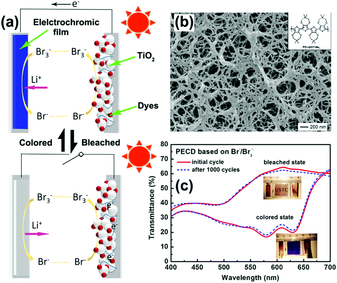 | ||
| Fig. 17 (a) Schematic design and working principle of a PECD employing a dye-adsorbed TiO2 nanoparticle film as the photoanode and an electropolymerized PProDOT-Me2 film as a cathode. (b) SEM image of the electropolymerized PProDOT-Me2 film. Reprinted from ref. 305. Copyright 2017 Springer. (c) Transmittance modulation and long-term cycling performance of the as-assembled PECD. Inset digital photos demonstrate the color contrast of the as-assembled PECD. Reprinted from ref. 304. Copyright 2016 Elsevier. | ||
8. Conclusions and outlook
Electrochromism has a wide range of applications in the various fields such as antireflection coatings, smart thermal control coatings, displays, and smart windows. Due to the fact that the electrochromism of metal oxides, hexacyanoferrates and conductive polymers comes from redox reactions, fabrication of self-supported 1D nanostructures becomes an effective category of morphologies to improve their performance due to their structural, electrochemical and processible advantages. The past few years have witnessed fast development and remarkable achievements of various morphologies and materials of self-supported 1D nanostructures for high electrochromism. Furthermore, apart from the basic function of electrochromism, additional functions have been successfully incorporated into electrochromic devices to broaden the devices’ functionality.To further accelerate the application of self-supported 1D nanostructures for electrochromism, some aspects may be improved by future study. (1) Investigation about the influence of morphology on the redox kinetics is desirable to be added. Better and deeper understanding of the relationship between the morphology and redox kinetics could give some useful guidance to design and prepare 1D nanostructures with desirable morphologies. (2) Fabrication of self-supported 1D nanostructures with high and reversible electrochromism derived from redox reactions of large-radius ions such as Na+, K+, Al3+, and Mg2+ is urgent, given the following facts: (I) economical favorability for large-scale applications due to the low cost and abundant metal resources; (II) different redox mechanisms and/or kinetics of large-radius ions compared to Li+ and H+; (III) the increasing popularity and economic requirement to develop materials and nanostructures for high Na+, K+, Al3+, and Mg2+ electrochemical energy storage devices such as batteries and supercapacitors.307–312 (3) Exploiting electrochromic materials with selective and independent optical modulation in the visible, NIR, and IR spectrum ranges is practically attractive. For smart window applications, the photons in the visible, NIR, and IR spectrum ranges carry different energies. Selective and independent optical modulation of a smart window in these different spectrum ranges could give multiple choices about selective control of indoor brightness and temperatures, making living more comfortable.151,232,313
Conflicts of interest
There are no conflicts to declare.Acknowledgements
We thank the National Natural Science Foundation of China (No. 51572058 and 51502057), the National Key Research & Development Program (2016YFB0303903), the Foundation of Science and Technology on Advanced Composites in Special Environment Laboratory, the Science and Technology Foundation of Guizhou Province of China (No. qian ke he ji chu [2017] 1065), the Scientific Research Starting Project of SWPU (2017QHZ019), and the Young Scholars Development Fund of SWPU (201799010003).References
- C. G. Granqvist, P. C. Lansåker, N. R. Mlyuka, G. A. Niklasson and E. Avendaño, Sol. Energy Mater. Sol. Cells, 2009, 93, 2032–2039 CrossRef CAS.
- D. R. Rosseinsky and R. J. Mortimer, Adv. Mater., 2001, 13, 783–793 CrossRef CAS.
- J. N. Yao, Y. A. Yang and B. H. Loo, J. Phys. Chem. B, 1998, 102, 1856–1860 CrossRef CAS.
- V. K. Thakur, G. Ding, J. Ma, P. S. Lee and X. Lu, Adv. Mater., 2012, 24, 4071–4096 CrossRef CAS PubMed.
- C. G. Granqvist, Thin Solid Films, 2016, 614, 90–96 CrossRef CAS.
- J. N. Tiwari, R. N. Tiwari and K. S. Kim, Prog. Mater. Sci., 2012, 57, 724–803 CrossRef CAS.
- R. S. Devan, R. A. Patil, J.-H. Lin and Y.-R. Ma, Adv. Funct. Mater., 2012, 22, 3326–3370 CrossRef CAS.
- B. L. Ellis, P. Knauth and T. Djenizian, Adv. Mater., 2014, 26, 3368–3397 CrossRef CAS PubMed.
- S. K. Deb, Appl. Opt., Suppl., 1969, 3, 192–195 CrossRef.
- S. F. Cogan, N. M. Nguyen, S. J. Perrotti and R. D. Rauh, J. Appl. Phys., 1989, 66, 1333 CrossRef CAS.
- C. G. Granqvist, Sol. Energy Mater. Sol. Cells, 2012, 99, 1–13 CrossRef CAS.
- T. Kobayashi, H. Yoneyama and H. Tamura, J. Electroanal. Chem., 1984, 161, 419–423 CrossRef CAS.
- C. M. Amb, A. L. Dyer and J. R. Reynolds, Chem. Mater., 2011, 23, 397–415 CrossRef CAS.
- S. Xiong, S. Yin, Y. Wang, Z. Kong, J. Lan, R. Zhang, M. Gong, B. Wu, J. Chu and X. Wang, Mater. Sci. Eng., B, 2017, 221, 41–53 CrossRef CAS.
- H. Zhang, G. Duan, G. Liu, Y. Li, X. Xu, Z. Dai, J. Wang and W. Cai, Nanoscale, 2013, 5, 2460–2468 RSC.
- R. Leones, R. C. Sabadini, F. C. Sentanin, J. M. S. S. Esperanç, A. Pawlicka and M. M. Silva, Sol. Energy Mater. Sol. Cells, 2017, 169, 98–106 CrossRef CAS.
- K. Wang, H. Wu, Y. Meng and Z. Wei, Small, 2014, 10, 14–31 CrossRef CAS PubMed.
- G. Cao and D. Liu, Adv. Colloid Interface Sci., 2008, 136, 45–64 CrossRef CAS PubMed.
- G. K. Mor, O. K. Varghese, M. Paulose, K. Shankar and C. A. Grimes, Sol. Energy Mater. Sol. Cells, 2006, 90, 2011–2075 CrossRef CAS.
- J. Martín, M. Martín-González, J. F. Fernández and O. Caballero-Calero, Nat. Commun., 2014, 5, 5130 CrossRef PubMed.
- H. Zhang, G. R. Li, L. P. An, T. Y. Yan, X. P. Gao and H. Y. Zhu, J. Phys. Chem. C, 2007, 111, 6143–6148 CAS.
- Y. Tang, Y. Zhang, J. Deng, J. Wei, H. L. Tam, B. K. Chandran, Z. Dong, Z. Chen and X. Chen, Adv. Mater., 2014, 26, 6111–6118 CrossRef CAS PubMed.
- K. Zhu, Q. Wang, J.-H. Kim, A. A. Pesaran and A. J. Frank, J. Phys. Chem. C, 2012, 116, 11895–11899 CAS.
- X. Lu, G. Wang, T. Zhai, M. Yu, J. Gan, Y. Tong and Y. Li, Nano Lett., 2012, 12, 1690–1696 CrossRef CAS PubMed.
- A. Dey, S. De, A. De and S. K. De, Nanotechnology, 2004, 15, 1277–1283 CrossRef CAS.
- Y.-C. Her and C.-C. Chang, CrystEngComm, 2014, 16, 5379–5386 RSC.
- X. H. Xia, J. P. Tu, J. Zhang, X. H. Huang, X. L. Wang, W. K. Zhang and H. Huang, Electrochem. Commun., 2009, 11, 702–705 CrossRef CAS.
- P. Yang, P. Sun and W. Mai, Mater. Today, 2016, 19, 394–402 CrossRef CAS.
- Z. Tong, Y. Tian, H. Zhang, X. Li, J. Ji, H. Qu, N. Li, J. Zhao and Y. Li, Sci. China: Chem., 2017, 60, 13–37 CrossRef CAS.
- Z. Yao, C. Wang, Y. Li and N.-Y. Kim, Nanoscale Res. Lett., 2015, 10, 166 CrossRef PubMed.
- H.-W. Shim, Y.-H. Jin, S.-D. Seo, S.-H. Lee and D.-W. Kim, ACS Nano, 2011, 5, 443–449 CrossRef CAS PubMed.
- H.-J. Zheng, X.-D. Wang and Z.-H. Gu, Acta Phys.-Chim. Sin., 2009, 25, 1650–1654 CAS.
- Z. Xiao, L. Zhang, X. Tian and X. Fang, Nanotechnology, 2005, 16, 2647–2650 CrossRef CAS.
- S. H. Park, J. Y. Song, H. M. Park and H. Yu, Mater. Res. Soc. Symp. Proc., 2010, 1258, 1258 Search PubMed.
- L. Guo, Y. Ren, J. Liu, S. Y. Chiam and W. K. Chim, Small, 2014, 10, 2611–2617 CrossRef CAS PubMed.
- K. Yamada, Y. Tanaka and S. Akimoto, Bull. Soc. Photogr. Imag. Jpn., 2015, 25, 38–40 Search PubMed.
- S. J. Limmer, K. Takahashi and G. Cao, Proc. SPIE., 2003, 25, 5224 Search PubMed.
- S. J. Limmer and G. Cao, Adv. Funct. Mater., 2003, 15, 427–431 CrossRef CAS.
- K. Takahashi, Y. Wang and G. Cao, Appl. Phys. Lett., 2005, 86, 053102 CrossRef.
- K. Takahashi, S. J. Limmer, Y. Wang and G. Cao, J. Phys. Chem. B, 2004, 108, 9795–9800 CrossRef CAS.
- J. Muster, G. T. Kim, V. Krstić, J. G. Park, Y. W. Park, S. Roth and M. Burghard, Adv. Mater., 2000, 12, 420–424 CrossRef CAS.
- Z. Miao, D. Xu, J. Ouyang, G. Guo, X. Zhao and Y. Tang, Nano Lett., 2002, 2, 717–720 CrossRef CAS.
- K. Takahashi, Y. Wang, K. Lee and G. Cao, Appl. Phys. A: Mater. Sci. Process., 2006, 82, 27–31 CrossRef CAS.
- Y. Wang and G. Cao, J. Mater. Chem., 2007, 17, 894–899 RSC.
- C. Yan, G. Chen, X. Zhou, J. Sun and C. Lv, Adv. Funct. Mater., 2016, 26, 1428–1436 CrossRef CAS.
- A. Al-Haddad, Z. Wang, R. Xu, H. Qi, R. Vellacheri, U. Kaiser and Y. Lei, J. Phys. Chem. C, 2015, 119, 16331–16337 CAS.
- Y. Zhang, M. Liu, W. Ren and Z.-G. Ye, Appl. Surf. Sci., 2015, 340, 120–125 CrossRef CAS.
- C. C. Chen, C.-H. Cheng and C.-K. Lin, Ceram. Int., 2013, 39, 6631–6636 CrossRef.
- L. Yuan, S. Meng, Y. Zhou and Z. Yue, J. Mater. Chem. A, 2013, 1, 2552–2557 CAS.
- Z. Liang, A. S. Susha, A. Yu and F. Caruso, Adv. Mater., 2003, 15, 1849–1853 CrossRef CAS.
- L. Li, S. Pan, X. Dou, Y. Zhu, X. Huang, Y. Yang, G. Li and L. Zhang, J. Phys. Chem. C, 2007, 111, 7288–7291 CAS.
- G. Y. Teo, M. P. Ryan and D. J. Riley, Electrochem. Commun., 2014, 47, 13–16 CrossRef CAS.
- H. Wang, Y. Song, W. Liu, S. Yao and W. Zhang, Mater. Lett., 2013, 93, 319–321 CrossRef CAS.
- N. M. Vuong, D. Kim and H. Kim, J. Mater. Chem. C, 2013, 1, 3399–3407 RSC.
- J. Liu, K. Song, P. A. van Aken, J. Maier and Y. Yu, Nano Lett., 2014, 14, 2597–2603 CrossRef CAS PubMed.
- J. Liu, Y. Li, H. Fan, Z. Zhu, J. Jiang, R. Ding, Y. Hu and X. Huang, Chem. Mater., 2010, 22, 212–217 CrossRef CAS.
- K. Wang, M. Wei, M. A. Morris, H. Zhou and J. D. Holmes, Adv. Mater., 2007, 17, 3016–3020 CrossRef.
- S. I. Cho and S. B. Lee, Acc. Chem. Res., 2008, 41, 699–707 CrossRef CAS PubMed.
- M. Xue, F. Li, D. Chen, Z. Yang, X. Wang and J. Ji, Adv. Mater., 2016, 28, 8265–8270 CrossRef CAS PubMed.
- Y. K. Hong, S. Kim, H. T. Kim, S. Kim, B.-G. Kim, S. Lee, D. H. Park and B.-H. Kim, Org. Electron., 2016, 32, 59–64 CrossRef CAS.
- Y.-Z. Long, M.-M. Li, C. Gu, M. Wan, J.-L. Duvail, Z. Liue and Z. Fan, Prog. Polym. Sci., 2011, 36, 1415–1442 CrossRef CAS.
- J. Duvail, Y. Long, S. Cuenot, Z. Chen and C. Gu, Appl. Phys. Lett., 2014, 90, 102114 CrossRef.
- Y. Long, L. Zhang, Z. Chen, K. Huang, Y. Yang and H. Xiao, Phys. Rev. B: Condens. Matter Mater. Phys., 2005, 71, 165412 CrossRef.
- S. Cuenot, S. Demoustier-Champagne and B. Nysten, Phys. Rev. Lett., 2000, 85, 1690 CrossRef CAS PubMed.
- S. I. Cho, W. J. Kwon, S.-J. Choi, P. Kim, S.-A. Park, J. Kim, S. J. Son, R. Xiao, S.-H. Kim and S. B. Lee, Adv. Mater., 2005, 17, 171–175 CrossRef CAS.
- H. Zhang, H. Qu, H. Lv, S. Hou, K. Zhang, J. Zhao, X. Li, E. Frank and Y. Li, Chem. – Asian J., 2016, 11, 2882–2888 CrossRef CAS PubMed.
- S. I. Cho, D. H. Choi, S.-H. Kim and S. B. Lee, Chem. Mater., 2005, 17, 4564–4566 CrossRef CAS.
- S. I. Cho, R. Xiao and S. B. Lee, Nanotechnology, 2007, 18, 405705 CrossRef.
- R. Xiao, S. I. Cho, R. Liu and S. B. Lee, J. Am. Chem. Soc., 2007, 129, 4483–4489 CrossRef CAS PubMed.
- S. Xiong, Q. Wang and H. Xia, Mater. Res. Bull., 2004, 39, 1569–1580 CrossRef CAS.
- C. Mijangos, R. Hernández and J. Martín, Prog. Polym. Sci., 2016, 54-55, 148–182 CrossRef CAS.
- L. Huang, Z. Wang, H. Wang, X. Cheng, A. Mitra and Y. Yan, J. Mater. Chem., 2002, 12, 388–391 RSC.
- J. I. Lee, S. H. Cho, S.-M. Park, J. K. Kim, J. K. Kim, J.-W. Yu, Y. C. Kim and T. P. Russell, Nano Lett., 2008, 8, 2315–2320 CrossRef CAS PubMed.
- G. Kimura and K. Yamada, Synth. Met., 2009, 159, 914–918 CrossRef CAS.
- Y. Kim, J. Baek, M.-H. Kim, H.-J. Choi and E. Kim, Ultramicroscopy, 2008, 108, 1224–1227 CrossRef CAS PubMed.
- Y. Kim, Y. Kim, S. Kim and E. Kim, ACS Nano, 2010, 4, 5277–5284 CrossRef CAS PubMed.
- R. B. Ambade, S. B. Ambade, N. K. Shrestha, R. R. Salunkhe, W. Lee, S. S. Bagde, J. H. Kim, F. J. Stadler, Y. Yamauchi and S.-H. Lee, J. Mater. Chem. A, 2017, 5, 172–180 CAS.
- M. Döbbelin, R. Tena-Zaera, P. M. Carrasco, J.-R. Sarasua, G. Cabañero and D. Mecerreyes, J. Polym. Sci., Part A: Polym. Chem., 2010, 48, 4648–4653 CrossRef.
- L. J. Pan, L. Pu, Y. Shi, S. Y. Song, Z. Xu, R. Zhang and Y. D. Zheng, Adv. Mater., 2007, 19, 461–464 CrossRef CAS.
- Z.-L. Wang, X.-J. He, S.-H. Ye, Y.-X. Tong and G.-R. Li, ACS Appl. Mater. Interfaces, 2014, 6, 642–647 CAS.
- U. Abacia, H. Y. Guney and U. Kadiroglu, Electrochim. Acta, 2013, 96, 214–224 CrossRef.
- W. Ap. Christinelli, A. B. Trench and E. C. Pereira, Sol. Energy Mater. Sol. Cells, 2016, 157, 703–708 CrossRef CAS.
- D. S. Dalavi, R. S. Devan, R. A. Patil, R. S. Patil, Y.-R. Ma, S. B. Sadale, I. Kim, J.-H. Kim and P. S. Patil, J. Mater. Chem. C, 2013, 1, 3722–3728 RSC.
- K. Ghosh, A. Roy, S. Tripathi, S. Ghule, A. K. Singh and N. Ravishankar, J. Mater. Chem. C, 2017, 5, 7307–7316 RSC.
- C. Y. Ng, K. A. Razak and Z. Lockman, Thin Solid Films, 2015, 595, 73–78 CrossRef CAS.
- F. Zheng, M. Guo and M. Zhang, CrystEngComm, 2013, 15, 277–284 RSC.
- C.-H. Lu, M. H. Hon and I.-C. Leu, J. Electron. Mater., 2017, 46, 2080–2084 CrossRef CAS.
- D. Ma, G. Shi, H. Wang, Q. Zhang and Y. Li, J. Mater. Chem. A, 2013, 1, 684–691 CAS.
- C.-H. Lu, M. H. Hon, C.-Y. Kuan and I.-C. Leu, J. Mater. Sci., 2015, 50, 5739–5745 CrossRef CAS.
- J. Zhang, J.-P. Tu, X.-H. Xia, X.-L. Wang and C.-D. Gu, J. Mater. Chem., 2011, 21, 5492–5498 RSC.
- C. J. Hung, Y. H. Huang, C. H. Chen, P. Lin and T. Y. Tseng, IEEE Trans. Compon., Packag., Manuf. Technol., 2014, 4, 831–838 CrossRef CAS.
- G. F. Cai, J. P. Tu, D. Zhou, X. L. Wang and C. D. Gu, Sol. Energy Mater. Sol. Cells, 2014, 124, 103–110 CrossRef CAS.
- C.-H. Lu, M.-H. Hon, C.-Y. Kuan and I.-C. Leu, RSC Adv., 2016, 6, 1913–1918 RSC.
- K. Hong, W. Yiu, H. Wu, J. Gao and M. Xie, Nanotechnology, 2005, 16, 1608–1611 CrossRef CAS.
- H. Wang, X. Quan, Y. Zhang and S. Chen, Nanotechnology, 2008, 19, 065704 CrossRef PubMed.
- J. Su, X. Feng, J. D. Sloppy, L. Guo and C. A. Grimes, Nano Lett., 2011, 11, 203–208 CrossRef CAS PubMed.
- R. Yu, Z. Meng, M. Ye, Y. Lin, N. Lin, X. Liu, W. Yu and X. Liu, CrystEngComm, 2015, 17, 6583–6590 RSC.
- N. Y. Bhosale, S. S. Mali, C. K. Hong and A. V. Kadam, Electrochim. Acta, 2017, 246, 1112–1120 CrossRef CAS.
- M. Shibuya and M. Miyauchi, Chem. Phys. Lett., 2009, 473, 126–130 CrossRef CAS.
- J. Zhang, X. L. Wang, X. H. Xia, C. D. Gu and J. P. Tu, Sol. Energy Mater. Sol. Cells, 2011, 95, 2107–2112 CrossRef CAS.
- V. V. Kondalkar, S. S. Mali, R. R. Kharade, K. V. Khot, P. B. Patil, R. M. Mane, S. Choudhury, P. S. Patil, C. K. Hong, J. H. Kim and P. N. Bhosale, Dalton Trans., 2015, 44, 2788–2800 RSC.
- D. Ma, T. Li, Z. Xu, L. Wang and J. Wang, Sol. Energy Mater. Sol. Cells, 2018, 177, 51–56 CrossRef CAS.
- H. Li, G. Shi, H. Wang, Q. Zhang and Y. Li, J. Mater. Chem. A, 2014, 2, 11305–11310 CAS.
- G. Cai, J. Tu, D. Zhou, L. Li, J. Zhang, X. Wang and C. Gua, CrystEngComm, 2014, 16, 6866–6872 RSC.
- S. Poongodi, P. S. Kumar, Y. Masuda, D. Mangalaraj, N. Ponpandian, C. Viswanathana and S. Ramakrishnad, RSC Adv., 2015, 5, 96416–96427 RSC.
- H. Li, J. Wang, G. Shi, H. Wang, Q. Zhang and Y. Li, RSC Adv., 2015, 5, 196–201 RSC.
- V. V. Kondalkar, R. R. Kharade, S. S. Mali, R. M. Mane, P. B. Patil, P. S. Patil, S. Choudhury and P. N. Bhosale, Superlattices Microstruct., 2014, 73, 290–295 CrossRef CAS.
- J. Chu, J. Lan, D. Lu, J. Ma, Xi. Wang, B. Wu, M. Gong, R. Zhang and S. Xiong, Micro Nano Lett., 2016, 11, 749–752 Search PubMed.
- Z. Jiao, X. W. Sun, J. Wang, L. Ke and H. V. Demir, J. Phys. D: Appl. Phys., 2010, 43, 285501 CrossRef.
- S. Adhikari and D. Sarkar, RSC Adv., 2014, 4, 20145–20153 RSC.
- Z. Jiao, J. Wang, L. Ke, X. Liu, H. V. Demir, M. F. Yang and X. W. Sun, Electrochim. Acta, 2012, 63, 153–160 CrossRef CAS.
- K. Lee, A. Mazare and P. Schmuki, Chem. Rev., 2014, 114, 9385–9454 CrossRef CAS PubMed.
- Z. Zhao, J. Tian, Y. Sang, A. Cabot and H. Liu, Adv. Mater., 2015, 27, 2557–2582 CrossRef CAS PubMed.
- S. H. Kang, S.-H. Choi, M.-S. Kang, J.-Y. Kim, H.-S. Kim, T. Hyeon and Y.-E. Sung, Adv. Mater., 2008, 20, 54–58 CrossRef CAS.
- B. H. Lee, M. Y. Song, S.-Y. Jang, S. M. Jo, S.-Y. Kwak and D. Y. Kim, J. Phys. Chem. C, 2009, 113, 21453–21457 CAS.
- B. Hao, Y. Yan, X. Wang and G. Chen, ACS Appl. Mater. Interfaces, 2013, 5, 6285–6291 CAS.
- B. Liu, J. E. Boercker and E. S. Aydil, Nanotechnology, 2008, 19, 505604 CrossRef CAS PubMed.
- J.-Z. Chen, W.-Y. Ko, Y.-C. Yen, P.-H. Chen and K.-J. Lin, ACS Nano, 2012, 8, 6633–6639 CrossRef PubMed.
- P. Qiang, Z. Chen, P. Yang, X. Cai, S. Tan, P. Liu and W. Mai, Nanotechnology, 2013, 24, 435403 CrossRef PubMed.
- S. Liu, X. Zhang, P. Sun, C. Wang, Y. Wei and Y. Liu, J. Mater. Chem. C, 2014, 2, 7891–7896 RSC.
- D. Lee, Y. Rho, F. I. Allen, A. M. Minor, S. H. Ko and C. P. Grigoropoulos, Nanoscale, 2013, 5, 11147–11152 RSC.
- H.-L. Chen and Y.-S. Yang, Thin Solid Films, 2008, 516, 5590–5596 CrossRef CAS.
- C.-S. Cheng, M. Serizawa, H. Sakata and T. Hirayama, Mater. Chem. Phys., 1998, 53, 225–230 CrossRef CAS.
- D. Zhou, D. Xie, X. Xia, X. Wang, C. Gu and J. Tu, Sci. China: Chem., 2017, 60, 3–12 CrossRef CAS.
- S. H. Park, J. W. Lim, S. J. Yoo, I. Y. Cha and Y.-E. Sung, Sol. Energy Mater. Sol. Cells, 2012, 99, 31–37 CrossRef CAS.
- Z. Chen, A. Xiao, Y. Chen, C. Zuo, S. Zhou and L. Li, J. Phys. Chem. Solids, 2013, 74, 1522–1526 CrossRef CAS.
- F. Cao, G. X. Pan, X. H. Xia, P. S. Tang and H. F. Chen, Electrochim. Acta, 2013, 111, 86–91 CrossRef CAS.
- C. Zhao, F. Du and J. Wang, RSC Adv., 2015, 5, 38706–38711 RSC.
- Y. Chen, Y. Wang, P. Sun, P. Yang, L. Du and W. Mai, J. Mater. Chem. A, 2015, 3, 20614–20618 CAS.
- Y. Li, B. Tan and Y. Wu, Nano Lett., 2008, 8, 265–270 CrossRef CAS PubMed.
- W. Mei, J. Huang, L. Zhu, Z. Ye, Y. Mai and J. Tu, J. Mater. Chem., 2012, 22, 9315–9321 RSC.
- X. Xia, J. Tu, Y. Mai, X. Wang, C. Gu and X. Zhao, J. Mater. Chem., 2011, 21, 9319–9325 RSC.
- Z. Wen, L. Zhu, W. Mei, L. Hu, Y. Li, L. Sun, H. Cai and Z. Ye, Sens. Actuators, B, 2013, 186, 172–179 CrossRef CAS.
- Y. Li, B. Tan and Y. Wu, Nano Lett., 2008, 8, 265–270 CrossRef CAS PubMed.
- S. Mishra, P. Yogi, S. Saxena, S. Roy, P. R. Sagdeo and R. Kumar, Adv. Mater. Processes Technol., 2017, 3, 627–631 Search PubMed.
- X. H. Xia, J. P. Tu, J. Zhang, J. Y. Xiang, X. L. Wang and X. B. Zhao, Sol. Energy Mater. Sol. Cells, 2010, 94, 386–389 CrossRef CAS.
- S. Elhag, Z. H. Ibupoto, X. Liu, O. Nur and M. Willander, Sens. Actuators, B, 2014, 203, 543–549 CrossRef CAS.
- N. A. Chernova, M. Roppolo, A. C. Dillon and M. S. Whittingham, J. Mater. Chem., 2009, 19, 2526–2552 RSC.
- V. Augustyn, P. Simon and B. Dunn, Energy Environ. Sci., 2014, 7, 1597–1614 CAS.
- Y. Lu, L. Liu, D. Mandler and P. S. Lee, J. Mater. Chem. C, 2013, 1, 7380–7386 RSC.
- S. D. Perera, B. Patel, J. Bonso, M. Grunewald, J. P. Ferraris and K. J. Balkus Jr., ACS Appl. Mater. Interfaces, 2011, 3, 4512–4517 CAS.
- G. Wang, X. Lu, Y. Ling, T. Zhai, H. Wang, Y. Tong and Y. Li, ACS Nano, 2012, 6, 10296–10302 CrossRef CAS PubMed.
- H. Wang, X. Gao, J. Feng and S. Xiong, Electrochim. Acta, 2015, 182, 769–774 CrossRef CAS.
- J. Chu, Z. Kong, D. Lu, W. Zhang, X. Wang, Y. Yu, S. Li, X. Wang, S. Xiong and J. Ma, Mater. Lett., 2016, 166, 179–182 CrossRef CAS.
- L. Zheng, Y. Xu, D. Jin and Y. Xie, J. Mater. Chem., 2010, 20, 7135–7143 RSC.
- B. Hui, G. Li, X. Zhao, L. Wang, D. Wu, J. Li and B. K. Via, J. Mater. Sci.: Mater. Electron., 2017, 28, 3264–3271 CrossRef CAS.
- X. W. Lou and H. C. Zeng, Chem. Mater., 2002, 14, 4781–4789 CrossRef CAS.
- L. Zheng, Y. Xu, D. Jin and Y. Xie, Chem. Mater., 2009, 21, 5681–5690 CrossRef CAS.
- L. Wang, X. Zhang, Y. Ma, M. Yang and Y. Qi, Mater. Lett., 2016, 164, 623–626 CrossRef CAS.
- D. Ma and J. Wang, Sci. China: Chem., 2017, 60, 54–62 CrossRef CAS.
- C. J. Dahlman, Y. Tan, M. A. Marcus and D. J. Milliron, J. Am. Chem. Soc., 2015, 137, 9160–9166 CrossRef CAS PubMed.
- Y. Zhan, M. R. J. Tan, X. Cheng, W. M. A. Tan, G. F. Cai, J. W. Chen, V. Kumar, S. Magdassi and P. S. Lee, J. Mater. Chem. C, 2017, 5, 9995–10000 RSC.
- S. Lou, Y. Ma, X. Cheng, J. Gao, Y. Gao, P. Zuo, C. Du and G. Yin, Chem. Commun., 2015, 51, 17293–17296 RSC.
- M. Najdoski, V. Koleva and A. Samet, J. Phys. Chem. C, 2014, 118, 9636–9646 CAS.
- X. Xiao, C. Zhang, S. Lin, L. Huang, Z. Hu, Y. Cheng, T. Li, W. Qiao, D. Long, Y. Huang, L. Mai, Y. Gogotsi and J. Zhou, Energy Storage Mater., 2015, 1, 1–8 CrossRef.
- K. Kalantar-zadeh, J. Z. Ou, T. Daeneke, A. Mitchell, T. Sasaki and M. S. Fuhrer, Appl. Mater. Today, 2016, 5, 73–89 CrossRef.
- J. Zhou, Y. Wei, G. Luo, J. Zheng and C. Xu, J. Mater. Chem. C, 2016, 4, 1613–1622 RSC.
- D. Zhou, F. Shi, D. Xie, D. H. Wang, X. H. Xia, X. L. Wang, C. D. Gu and J. P. Tu, J. Colloid Interface Sci., 2016, 465, 112–120 CrossRef CAS PubMed.
- G. Hodes, Phys. Chem. Chem. Phys., 2007, 9, 2181–2196 RSC.
- X. H. Xia, J. P. Tu, J. Zhang, X. H. Huang, X. L. Wang, W. K. Zhang and H. Huang, Electrochem. Commun., 2008, 10, 1815–1818 CrossRef CAS.
- M. Z. Najdoski and T. Todorovski, Mater. Chem. Phys., 2007, 104, 483–487 CrossRef CAS.
- T. Berger, T. Lana-Villarreal, D. Monllor-Satoca and R. Gómez, Chem. Phys. Lett., 2007, 447, 91–95 CrossRef CAS.
- M. Najdoski, V. Koleva and S. Demiri, Mater. Res. Bull., 2012, 47, 737–743 CrossRef CAS.
- X. H. Xia, J. P. Tu, J. Zhang, X. L. Wang, W. K. Zhang and H. Huang, Sol. Energy Mater. Sol. Cells, 2008, 92, 628–633 CrossRef CAS.
- S. Akinkuade, B. Mwankemwa, J. Nel and W. Meyer, Physica B, 2017 DOI:10.1016/j.physb.2017.06.021.
- E. Hosono, S. Fujihara, I. Honmaa and H. Zhou, J. Mater. Chem., 2005, 15, 1938–1945 RSC.
- B. Li, J.-M. Wu, T.-T. Guo, M.-Z. Tang and W. Wen, Nanoscale, 2014, 6, 3046–3050 RSC.
- A. Dhara, G. Hodes and S. K. Sarkar, RSC Adv., 2014, 4, 53694–53700 RSC.
- R. S. Devan, R. A. Patil, J.-H. Lin and Y.-R. Ma, Adv. Funct. Mater., 2012, 22, 3326–3370 CrossRef CAS.
- J. M. Velazquez and S. Banerjee, Small, 2009, 5, 1025–1029 CrossRef CAS PubMed.
- L.-C. Tien and Y.-J. Chen, Appl. Surf. Sci., 2012, 258, 3584–3588 CrossRef CAS.
- C.-C. Liao, F.-R. Chen and J.-J. Kai, Sol. Energy Mater. Sol. Cells, 2007, 91, 1258–1266 CrossRef CAS.
- R. Nechache, M. Nicklaus, N. Diffalah, A. Ruediger and F. Rosei, Appl. Surf. Sci., 2014, 313, 48–52 CrossRef CAS.
- S. M. Nicaise, J. J. Cheng, A. Kiani, S. Gradečak and K. K. Berggren, Nanotechnology, 2015, 26, 075303 CrossRef PubMed.
- R. K. Sharma, P. Kumar and G. B. Reddy, J. Alloys Compd., 2015, 638, 289–297 CrossRef CAS.
- K.-C. Cheng, F.-R. Chen and J.-J. Kai, Sol. Energy Mater. Sol. Cells, 2006, 90, 1156–1165 CrossRef CAS.
- C.-C. Liao, F.-R. Chen and J.-J. Kai, Sol. Energy Mater. Sol. Cells, 2006, 90, 1147–1155 CrossRef CAS.
- L. Xiao, Y. Lv, W. Dong, N. Zhang and X. Liu, ACS Appl. Mater. Interfaces, 2016, 8, 27107–27114 CAS.
- S. Gubbala, J. Thangala and M. K. Sunkara, Sol. Energy Mater. Sol. Cells, 2007, 91, 813–820 CrossRef CAS.
- J. Thangala, S. Vaddiraju, R. Bogale, R. Thurman, T. Powers, B. Deb and M. K. Sunkara, Small, 2007, 3, 890–896 CrossRef CAS PubMed.
- R. S. Devan, S.-Y. Gao, W.-D. Ho, J.-H. Lin, Y.-R. Ma, P. S. Patil and Y. Liou, Appl. Phys. Lett., 2011, 98, 133117 CrossRef.
- P. Meduri, E. Clark, J. H. Kim, E. Dayalan, G. U. Sumanasekera and Ma. K. Sunkara, Nano Lett., 2012, 12, 1784–1788 CrossRef CAS PubMed.
- M.-C. Wu and C.-S. Lee, J. Solid State Chem., 2009, 182, 2285–2289 CrossRef CAS.
- R. A. Patil, R. S. Devan, J.-H. Lin, Y.-R. Ma, P. S. Patil and Y. Liou, Sol. Energy Mater. Sol. Cells, 2013, 112, 91–96 CrossRef CAS.
- R. A. Patil, R. S. Devan, Y. Liou and Y.-R. Ma, Sol. Energy Mater. Sol. Cells, 2016, 147, 240–245 CrossRef CAS.
- M. Z. Sialvi, R. J. Mortimer, G. D. Wilcox, A. M. Teridi, T. S. Varley, K. G. U. Wijayantha and C. A. Kirk, ACS Appl. Mater. Interfaces, 2013, 5, 5675–5682 CAS.
- T. Stoycheva, F. E. Annanouch, I. Gràcia, E. Llobet, C. Blackman, X. Correig and S. Vallejos, Sens. Actuators, B, 2014, 198, 210–218 CrossRef CAS.
- H. Kim, R. O. Bonsu, C. O’Donohue, R. Y. Korotkov, L. McElwee-White and T. J. Anderson, ACS Appl. Mater. Interfaces, 2015, 7, 2660–2667 CAS.
- D. Kowalskia, D. Kim and P. Schmuki, Nano Today, 2013, 8, 235–264 CrossRef.
- N. A. Kyeremateng, F. Vacandio, M.-T. Sougrati, H. Martinez, J.-C. Jumas, P. Knauth and T. Djenizian, J. Power Sources, 2013, 224, 269–277 CrossRef CAS.
- A. Ghicov, H. Tsuchiya, R. Hahn, J. M. Macak, A. G. Muñoz and P. Schmuki, Electrochem. Commun., 2006, 8, 528–532 CrossRef CAS.
- R. Hahn, A. Ghicov, H. Tsuchiya, J. M. Macak, A. G. Muñoz and P. Schmuki, Phys. Status Solidi A, 2007, 204, 1281–1285 CrossRef CAS.
- Y. Yang, D. Kim and P. Schmuki, Electrochem. Commun., 2011, 13, 1198–1201 CrossRef CAS.
- Y.-C. Nah, A. Ghicov, D. Kim, S. Berger and P. Schmuki, J. Am. Chem. Soc., 2008, 130, 16154–16155 CrossRef CAS PubMed.
- A. Ghicov, M. Yamamoto and P. Schmuki, Angew. Chem., Int. Ed., 2008, 47, 7934–7937 CrossRef CAS PubMed.
- Y. Yang, D. Kim and P. Schmuki, Electrochem. Commun., 2011, 13, 1021–1025 CrossRef CAS.
- N. K. Shrestha, Y.-C. Nah, H. Tsuchiy and P. Schmuki, Chem. Commun., 2009, 2008–2010 RSC.
- R. Kirchgeorg, S. Berger and P. Schmuki, Chem. Commun., 2011, 47, 1000–1002 RSC.
- S. Adhikari, Y.-Y. Song, Y.-M. Wang, M. Niraula, K. Cho, S. K. Dhungel, Z.-D. Gao, N. K. Shrestha and S.-H. Han, Opt. Mater., 2015, 40, 112–117 CrossRef CAS.
- A. Benoit, I. Paramasivam, Y.-C. Nah, P. Roy and P. Schmuki, Electrochem. Commun., 2009, 11, 728–732 CrossRef CAS.
- N. K. Shrestha, M. Yang and P. Schmukiz, Electrochem. Solid-State Lett., 2010, 13, C21–C24 CrossRef CAS.
- J. Z. Ou, S. Balendhran, M. R. Field, D. G. McCulloch, A. S. Zoolfakar, R. A. Rani, S. Zhuiykov, A. P. O'Mullane and K. Kalantar-zadeh, Nanoscale, 2012, 4, 5980–5988 RSC.
- S. Berger, A. Ghicov, Y.-C. Nah and P. Schmuki, Langmuir, 2009, 25, 4841–4844 CrossRef CAS PubMed.
- X. Yang, X. Wei, S. Wu, T. Wu, Z. Chen and S. Li, J. Mater. Sci.: Mater. Electron., 2015, 26, 7081–7085 CrossRef CAS.
- S. Barredo-Damas, K. Lee, R. Kirchgeorg, R. Sánchez-Tovar and P. Schmuki, ECS Electrochem. Lett., 2013, 2, C4–C6 CrossRef CAS.
- D. D. Yao, M. R. Field, A. P. O'Mullane, K. Kalantar-zadeh and J. Z. Ou, Nanoscale, 2013, 5, 10353–10359 RSC.
- D. Guan, J. Li, X. Gao and C. Yuan, RSC Adv., 2014, 4, 4055–4062 RSC.
- D. D. Yao, R. A. Rani, A. P. O’Mullane, K. Kalantar-zadeh and J. Z. Ou, J. Phys. Chem. C, 2014, 118, 10867–10873 CAS.
- D. D. Yao, R. A. Rani, A. P. O’Mullane, K. Kalantar-zadeh and J. Z. Ou, J. Phys. Chem. C, 2014, 118, 476–481 CAS.
- J. Zhang, X. L. Wang, X. H. Xia, C. D. Gu, Z. J. Zhao and J. P. Tu, Electrochim. Acta, 2010, 55, 6953–6958 CrossRef CAS.
- J. Lin, X. Liu, M. Guo, W. Lu, G. Zhang, L. Zhou, X. Chen and H. Huang, Nanoscale, 2012, 4, 5148–5153 RSC.
- I. S. Cho, J. Choi, K. Zhang, S. J. Kim, M. J. Jeong, L. Cai, T. Park, X. Zheng and J. H. Park, Nano Lett., 2015, 15, 5709–5715 CrossRef CAS PubMed.
- H. Lv, N. Li, H. Zhang, Y. Tian, H. Zhang, X. Zhang, H. Qu, C. Liu, C. Jia, J. Zhao and Y. Li, Sol. Energy Mater. Sol. Cells, 2016, 150, 57–64 CrossRef CAS.
- K. R. Reyes-Gil, Z. D. Stephens, V. Stavila and D. B. Robinso, ACS Appl. Mater. Interfaces, 2015, 7, 2202–2213 CAS.
- Z. Tong, J. Hao, K. Zhang, J. Zhao, B.-L. Su and Y. Li, J. Mater. Chem. C, 2014, 2, 3651–3658 RSC.
- Z. Tong, H. Yang, L. Na, H. Qu, X. Zhang, J. Zhao and Y. Li, J. Mater. Chem. C, 2015, 3, 3159–3166 RSC.
- Z. Tong, H. Xu, G. Liu, J. Zhao and Y. Li, Electrochem. Commun., 2016, 69, 46–49 CrossRef CAS.
- Z. Tong, X. Zhang, H. Lv, N. Li, H. Qu, J. Zhao, Y. Li and X.-Y. Liu, Adv. Mater. Interfaces, 2015, 2, 1500230 CrossRef.
- Z. Tong, N. Li, H. Lv, Y. Tian, H. Qu, X. Zhang, J. Zhao and Y. Li, Sol. Energy Mater. Sol. Cells, 2016, 146, 135–143 CrossRef CAS.
- Z. Tong, H. Lv, X. Zhang, H. Yang, Y. Tian, N. Li, J. Zhao and Y. Li, Sci. Rep., 2015, 5, 16864 CrossRef CAS PubMed.
- M. Alsawafta, A. Almoabadi, S. Badilescu and V.-V. Truong, J. Electrochem. Soc., 2015, 162, H466–H472 CrossRef CAS.
- C.-S. Hsu, C.-C. Chan, H.-T. Huang, C.-H. Peng and W.-C. Hsu, Thin Solid Films, 2008, 516, 4839–4844 CrossRef CAS.
- M. Dhanasankar, K. K. Purushothaman and G. Muralidharan, Solid State Sci., 2010, 12, 246–251 CrossRef CAS.
- S. Cong, T. Sugahara, T. Wei, J. Jiu, Y. Hirose, S. Nagao and K. Suganuma, Cryst. Growth Des., 2015, 15, 4536–4542 CAS.
- C. Yan and D. Xue, Adv. Mater., 2008, 20, 1055–1058 CrossRef CAS.
- L. He, Z. Li and Z. Zhang, Nanotechnology, 2008, 19, 155606 CrossRef PubMed.
- K. K. Purushothaman and G. Muralidharan, Sol. Energy Mater. Sol. Cells, 2009, 93, 1195–1201 CrossRef CAS.
- R. Seelaboyina, Nanotechnology, 2016, 27, 112502 CrossRef PubMed.
- H. Tokudome and M. Miyauchi, Angew. Chem., Int. Ed., 2005, 44, 1974–1977 CrossRef CAS PubMed.
- C. Xiong, A. E. Aliev, B. Gnade and K. J. Balkus, Jr., ACS Nano, 2008, 2, 293–301 CrossRef CAS PubMed.
- W. Kang, C. Yan, X. Wang, C. Y. Foo, A. W. M. Tan, K. J. Z. Chee and P. S. Lee, J. Mater. Chem. C, 2014, 2, 4727–4732 RSC.
- S. Heo, J. Kim, G. K. Ong and D. J. Milliron, Nano Lett., 2017, 17, 5756–5761 CrossRef CAS PubMed.
- P. Yang and F. Kim, ChemPhysChem, 2002, 3, 503–506 CrossRef CAS PubMed.
- F. Pan, J. Zhang, C. Cai and T. Wang, Langmuir, 2006, 22, 7101–7104 CrossRef CAS PubMed.
- S. J. Yoo, Y. H. Jung, J. W. Lim, H. G. Choi, D. K. Kim and Y.-E. Sung, Sol. Energy Mater. Sol. Cells, 2008, 92, 179–183 CrossRef CAS.
- X. Changa, S. Suna, Z. Li, X. Xu and Y. Qiu, Appl. Surf. Sci., 2011, 257, 5726–5730 CrossRef.
- J. Wang, E. Khoo, P. S. Lee and J. Ma, J. Phys. Chem. C, 2008, 112, 14306–14312 CAS.
- J.-W. Liu, J. Zheng, J.-L. Wang, J. Xu, H.-H. Li and S.-H. Yu, Nano Lett., 2013, 13, 3589–3593 CrossRef PubMed.
- J.-L. Wang, Y.-R. Lu, H.-H. Li, J.-W. Liu and S.-H. Yu, J. Am. Chem. Soc., 2017, 139, 9921–9926 CrossRef CAS PubMed.
- D. N. Nguyen and H. Yoon, Polymers, 2016, 8, 118 CrossRef.
- L. Zhao, L. Zhao, Y. Xu, T. Qiu, L. Zhi and G. Shi, Electrochim. Acta, 2009, 55, 491–497 CrossRef CAS.
- S. Yunus, A. Attout and P. Bertrand, Langmuir, 2009, 25, 1851–1854 CrossRef CAS PubMed.
- S. Zhang, R. Fu, S. Wang, Y. Gu and S. Chen, Mater. Lett., 2017, 202, 127–130 CrossRef CAS.
- L. Zhang and M. Wan, Nanotechnology, 2002, 13, 750–755 CrossRef CAS.
- K. Wang, P. Zhao, X. Zhou, H. Wu and Z. Wei, J. Mater. Chem., 2011, 21, 16373–16378 RSC.
- N.-R. Chiou, C. Lu, J. Guan, L. J. Lee and A. J. Epstein, Nat. Nanotechnol., 2007, 2, 354–357 CrossRef CAS PubMed.
- K. Wang, W. Zou, B. Quan, A. Yu, H. Wu, P. Jiang and Z. Wei, Adv. Energy Mater., 2011, 1, 1068–1072 CrossRef CAS.
- Y. Wang, S. Xu, H. Cheng, W. Liu, F. Chen, X. Liu, J. Liu, S. Chen and C. Hu, Appl. Surf. Sci., 2018, 428, 315–321 CrossRef CAS.
- J. Desilvestro and W. Scheifele, J. Mater. Chem., 1993, 3, 263–272 RSC.
- Z. Tong, H. Lv, J. Zhao and Y. Li, Chin. J. Polym. Sci., 2014, 32, 1040–1051 CrossRef CAS.
- K. Wang, J. Huang and Z. Wei, J. Phys. Chem. C, 2010, 114, 8062–8067 CAS.
- J. Huang, K. Wang and Z. Wei, J. Mater. Chem., 2010, 20, 1117–1121 RSC.
- S. Jiang, B. Yi, L. Cao, W. Song, Q. Zhao, H. Yu and Z. Shao, J. Power Sources, 2016, 329, 347–354 CrossRef CAS.
- E. M. Erro, A. M. Baruzzi and R. A. Iglesias, Polymer, 2014, 55, 2440–2444 CrossRef CAS.
- Y. E. Firat and A. Peksoz, J. Mater. Sci.: Mater. Electron., 2017, 28, 3515–3522 CrossRef CAS.
- R. M. Osuna, V. Hernández, J. T. L. Navarrete, E. I. Kauppinen and V. Ruiz, J. Phys. Chem. Lett., 2010, 1, 1367–1371 CrossRef.
- A. Antonaia, M. L. Addonizio, C. Minarini, T. Polichetti and M. Vittori-Antisari, Electrochim. Acta, 2001, 46, 2221–2227 CrossRef CAS.
- M. Deepa, A. G. Joshi, A. K. Srivastava, S. M. Shivaprasad and S. A. Agnihotry, J. Electrochem. Soc., 2006, 153, C365–C376 CrossRef CAS.
- H.-T. Fang, M. Liu, D.-W. Wang, T. Sun, D.-S. Guan, F. Li, J. Zhou, T.-K. Sham and H.-M. Cheng, Nanotechnology, 2009, 20, 225701 CrossRef PubMed.
- H. Qu, X. Zhang, L. Pan, Z. Gao, L. Ma, J. Zhao and Y. Li, Electrochim. Acta, 2014, 148, 46–52 CrossRef CAS.
- D. Zhou, D. Xie, F. Shi, D. H. Wang, X. Ge, X. H. Xia, X. L. Wang, C. D. Gu and J. P. Tu, J. Colloid Interface Sci., 2015, 460, 200–208 CrossRef CAS PubMed.
- Y. Chen, X. Li, Z. Bi, X. He, X. Xu and X. Gao, Electrochim. Acta, 2017, 251, 546–553 CrossRef CAS.
- W. Dong, Y. Lv, L. Xiao, Y. Fan, N. Zhang and X. Liu, ACS Appl. Mater. Interfaces, 2016, 8, 33842–33847 CAS.
- M. Wang, G. Fang, L. Yuan, H. Huang, Z. Sun, N. Liu, S. Xia and X. Zhao, Nanotechnology, 2009, 20, 185304 CrossRef PubMed.
- Z. Bi, X. Li, Y. Chen, X. Xu, S. Zhang and Q. Zhu, Electrochim. Acta, 2017, 227, 6–68 CrossRef.
- J. Zhang, J. Tu, D. Zhou, H. Tang, L. Li, X. Wang and C. Gu, J. Mater. Chem. C, 2014, 2, 10409–10417 RSC.
- Y. Liu, C. Jia, Z. Wan, X. Weng, J. Xie and L. Deng, Sol. Energy Mater. Sol. Cells, 2015, 132, 467–475 CrossRef CAS.
- B.-R. Huang, T.-C. Lin and Y.-M. Liu, Sol. Energy Mater. Sol. Cells, 2015, 133, 32–38 CrossRef CAS.
- L. Cheng, X. Zhang, B. Liu, H. Wang, Y. Li, Y. Huang and Z. Du, Nanotechnology, 2005, 16, 1341–1345 CrossRef CAS.
- G. Cai, J. Tu, D. Zhou, L. Li, J. Zhang, X. Wang and C. Gu, J. Phys. Chem. C, 2014, 118, 6690–6696 CAS.
- G. Bo, X. Wang, K. Wang, R. Gao, B. Dong, L. Cao and G. Su, J. Alloys Compd., 2017, 728, 878–886 CrossRef CAS.
- G. F. Cai, D. Zhou, Q. Q. Xiong, J. H. Zhang, X. L. Wang, C. D. Gu and J. P. Tu, Sol. Energy Mater. Sol. Cells, 2013, 117, 231–238 CrossRef CAS.
- Y. Li, Z. Liu, L. Zhao, T. Cui, B. Wang, K. Guo and J. Han, Electrochim. Acta, 2015, 173, 117–123 CrossRef CAS.
- Y. Dong, C. Xiong, Y. Zhang, S. Xing and H. Jiang, Nanotechnology, 2016, 27, 105704 CrossRef PubMed.
- W. He, Y. Liu, Z. Wan and C. Jia, RSC Adv., 2016, 6, 68997–69006 RSC.
- H. Yu, Y. Li, L. Zhao, G. Li, J. Li, H. Rong and Z. Liu, Mater. Lett., 2016, 169, 65–68 CrossRef CAS.
- A. P. Baioni, M. Vidotti, P. A. Fiorito, E. A. Ponzio and S. I. Córdoba de Torresi, Langmuir, 2007, 23, 6796–6800 CrossRef CAS PubMed.
- K.-M. Lee, H. Tanaka, A. Takahashi, K. H. Kim, M. Kawamura, Y. Abe and T. Kawamoto, Electrochim. Acta, 2015, 163, 288–295 CrossRef CAS.
- H.-Y. Liao, T.-C. Liao, W.-H. Chen, C.-H. Chang and L.-C. Chen, Sol. Energy Mater. Sol. Cells, 2016, 145, 8–15 CrossRef CAS.
- Y. Chen, Z. Bi, X. Li, X. Xu, S. Zhang and X. Hu, Electrochim. Acta, 2017, 224, 534–540 CrossRef CAS.
- S.-M. Wang, L. Liu, W.-L. Chen, Z.-M. Zhang, Z.-M. Su and E.-B. Wang, J. Mater. Chem. A, 2013, 1, 216–220 CAS.
- B. Zhang, W. Guan, S. Zhang, B. Li and L. Wu, Chem. Commun., 2016, 52, 5308–5311 RSC.
- S. Liu and X. Qu, Appl. Surf. Sci., 2017, 412, 189–195 CrossRef CAS.
- C. Zhou, Y. Zhang, Y. Li and J. Liu, Nano Lett., 2013, 13, 2078–2085 CrossRef CAS PubMed.
- Z. Tong, Y. Yang, J. Wang, J. Zhao, B.-L. Su and Y. Li, J. Mater. Chem. A, 2014, 2, 4642–4651 CAS.
- X. Xia, D. Chao, X. Qi, Q. Xiong, Y. Zhang, J. Tu, H. Zhang and H. J. Fan, Nano Lett., 2013, 13, 4562–4568 CrossRef CAS PubMed.
- Z. Tong, S. Liu, X. Li, Y. Ding, J. Zhao and Y. Li, Electrochim. Acta, 2016, 222, 194–202 CrossRef CAS.
- X. H. Xia, J. P. Tu, J. Zhang, X. L. Wang, W. K. Zhang and H. Huang, Nanotechnology, 2008, 19, 465701 CrossRef CAS PubMed.
- G. Cai, J. Tu, D. Zhou, J. Zhang, Q. Xiong, X. Zhao, X. Wang and C. Gu, J. Phys. Chem. C, 2013, 117, 15967–15975 CAS.
- X. Fu, C. Jia, Z. Wan, X. Weng, J. Xie and L. Deng, Org. Electron., 2014, 15, 2702–2709 CrossRef CAS.
- G. F. Cai, J. P. Tu, D. Zhou, J. H. Zhang, X. L. Wang and C. D. Gu, Sol. Energy Mater. Sol. Cells, 2014, 122, 51–58 CrossRef CAS.
- D. Ma, G. Shi, H. Wang, Q. Zhang and Y. Li, J. Mater. Chem. A, 2014, 2, 13541–13549 CAS.
- C. Dulgerbaki, N. N. Maslakci, A. I. Komur and A. U. Oksuz, Electroanalysis, 2016, 28, 1873–1879 CrossRef CAS.
- M. Kateb, S. Safarian, M. Kolahdouz, M. Fathipour and V. Ahamdi, Sol. Energy Mater. Sol. Cells, 2016, 145, 200–205 CrossRef CAS.
- J.-C. Chou, C.-J. Yang, Y.-H. Liao, P.-A. Ho, H.-T. Chou and C.-H. Huang, J. Disp. Technol., 2015, 11, 430–437 CrossRef CAS.
- K. Zhang, Y. Wang, X. Ma, H. Zhang, S. Hou, J. Zhao, X. Li, L. Qiang and Y. Li, New J. Chem., 2017, 41, 10872–10879 RSC.
- X. W. Sun and J. X. Wang, Nano Lett., 2008, 8, 1884–1889 CrossRef CAS PubMed.
- A. Hua, F. Wu, J. Liu, J. Jiang, R. Ding, X. Li, C. Cheng, Z. Zhu and X. Huang, J. Alloys Compd., 2010, 507, 261–266 CrossRef.
- S. Li, Y. Wang, J.-G. Wu, L. Guo, M. Ye, Y.-H. Shao, R. Wang, C. Zhao and A. Wei, RSC Adv., 2016, 6, 72037–72043 RSC.
- G. Cai, J. Wang and P. S. Lee, Acc. Chem. Res., 2016, 49, 1469–1476 CrossRef CAS PubMed.
- K. Wang, H. Wu, Y. Meng, Y. Zhang and Z. Wei, Energy Environ. Sci., 2012, 5, 8384–8389 CAS.
- Z. Tong, S. Liu, X. Li, L. Mai, J. Zhao and Y. Li, Nanoscale, 2018, 10, 3254–3261 RSC.
- J.-J. Wu, M.-D. Hsieh, W.-P. Liao, W.-T. Wu and J.-S. Chen, ACS Nano, 2009, 3, 2297–2303 CrossRef CAS PubMed.
- X. Wu, J. Zheng and C. Xu, Electrochim. Acta, 2016, 191, 902–907 CrossRef CAS.
- X. Wu, J. Zheng and C. Xu, Sci. China: Chem., 2017, 60, 84–89 CrossRef CAS.
- X. F. Yu, Y. X. Li, N. F. Zhu, Q. B. Yang and K. Kalantar-zadeh, Nanotechnology, 2007, 18, 015201 CrossRef.
- Y. Tian, W. Zhang, S. Cong, Y. Zheng, F. Geng and Z. Zhao, Adv. Funct. Mater., 2015, 25, 5833–5839 CrossRef CAS.
- Z. Tong, S. Liu, Y. Zhou, J. Zhao, Y. Wu, Y. Wang and Y. Li, Energy Storage Mater., 2018, 13, 223–232 CrossRef.
- S. Lou, X. Cheng, J. Gao, Q. Li, L. Wang, Y. Cao, Y. Ma, P. Zuo, Y. Gao, C. Du, H. Huo and G. Yin, Energy Storage Mater., 2018, 11, 57–66 CrossRef.
- S. Lou, X. Cheng, L. Wang, J. Gao, Q. Li, Y. Ma, Y. Gao, P. Zuo, C. Du and G. Yin, J. Power Sources, 2017, 361, 80–86 CrossRef CAS.
- S. Lou, X. Cheng, Y. Zhao, A. Lushington, J. Gao, Q. Li, P. Zuo, B. Wang, Y. Gao, Y. Ma, C. Du, G. Yin and X. Sun, Nano Energy, 2017, 34, 15–25 CrossRef CAS.
- Y. Huang, X. Li, J. Luo, K. Wang, Q. Zhang, Y. Qiu, S. Sun, S. Liu, J. Han and Y. Huang, ACS Appl. Mater. Interfaces, 2017, 9, 8696–8703 CAS.
- A. Llordés, G. Garcia, J. Gazquez and D. J. Milliron, Nature, 2013, 500, 323–326 CrossRef PubMed.
Footnote |
| † These two authors contributed equally to this work. |
| This journal is © The Royal Society of Chemistry 2018 |