
 Open Access Article
 This Open Access Article is licensed under a Creative Commons Attribution-Non Commercial 3.0 Unported Licence
Polystyrene enhanced crystallization of perovskites towards high performance solar cells†
Hyeong Pil
Kim
a,
Abd. Rashid
bin Mohd Yusoff
 b and
Jin
Jang
*a
b and
Jin
Jang
*a
aAdvanced Display Research Center, Department of Information Display, Kyung Hee University, Dongdaemoon-gu, Seoul 130-701, South Korea. E-mail: hpkim@khu.ac.kr; jjang@khu.ac.kr
bDepartment of Materials Science & Engineering, Yonsei University, Seoul 03722, South Korea. E-mail: abdr@yonsei.ac.kr
First published on 29th August 2018
Abstract
Perovskite solar cells have attracted significant attention due to their high efficiency and low cost. In the research on methylammonium lead-iodide (CH3NH3PbI3), a lot of work has been devoted to optimize the film morphology and crystallinity resulting in an enhancement of the power conversion efficiency (PCE). A good surface coverage and uniform perovskite films are highly desirable along with a smooth and pinhole-free contact between the hole and electron extraction layers. Overall, this affects the charge transport and collection, and reduces charge recombination. Herein, we demonstrate a facile route to control perovskite crystallization by inserting an optimal amount of insulating polystyrene in the perovskite precursor solutions. The incorporation of a small amount of polystyrene results in much better surface coverage, and a smoother and uniform perovskite thin film leading to improved crystallization and larger grain size. Via careful optimization, and easy and low temperature solution-based processing, below 100 °C, we realize a device with PCE exceeding 13% along with significantly reduced leakage current.
Introduction
Today, methylammonium lead halide perovskite (CH3NH3PbI3) is one of the most extensively studied photovoltaic materials for high performance, low-temperature solution-processable perovskite solar cells. Perovskite solar cells offer copious advantages over existing technologies namely ambipolar charge transport property, wide range light absorption with high extinction coefficients and long electron–hole diffusion length.1–14 Perovskite technology started in 2009 when Miyasaka et al. constructed a dye-sensitized solar cell employing a mesoporous titanium dioxide (TiO2) electron transport layer (ETL) and CH3NH3PbI3 as a light absorber.2 Since 2009, huge progress has been reported mainly via device and interface engineering in the mesoporous configuration. In parallel, a planar heterojunction configuration has also been developed as the most straightforward structure getting rid of the mesoporous metal oxide.10 Both n-i-p and p-i-n structures have been then further optimized owing to the ambipolar property of the perovskite.8 Despite a simple fabrication process, n-i-p based CH3NH3PbI3 planar devices sandwiched between TiO2 and HTL encountered a serious hysteresis issue compared to their counterpart p-i-n based devices. p-i-n based CH3NH3PbI3 planar devices show reduced current hysteresis mainly due to the balanced hole and electron diffusion length in CH3NH3PbI3.1–14 However, despite significant advancements made to date, the performance of p-i-n CH3NH3PbI3 based solar cells usually employing poly(3,4-ethylenedioxythiophene):polystyrene sulfonate (PEDOT:PSS) or nickel oxide (NiO) is still far behind that of n-i-p CH3NH3PbI3 based solar cells. The main concern is the ability to control the perovskite crystallization process, and subsequently film formation and quality. Film morphology has a direct impact on device performance affecting charge trapping, recombination, transport, and extraction pathways.15–18 In general, the crystal nucleation and film growth depend on various factors such as deposition temperature, selection of solvent, precursor composition, solution concentration and interfacial energy. For instance, several groups had previously reported on the beneficial effect of the pre-deposition of PbI2 from solution onto mesoporous TiO2 to improve perovskite thin film crystallinity due to9 improved perovskite nucleation at the mesoporous TiO2 surface. Moreover, Snaith et al. also reported that perovskite crystallization rate can be controlled by varying precursor composition.5,12,17,19–30 For instance, in the case of CH3NH3PbI3 the crystallization is further prolonged by partially replacing I− with Cl− due to the lattice distortion caused by the Cl− ion.31aIn this work, we demonstrate a facile and attractive route to enhance the crystallization and grain size of the perovskite absorber, and subsequently improve the performances of perovskite solar cells. We found that the crystallization rate of perovskite can be effectively tuned by integrating insulating polystyrene (PS) into its precursor solution to modulate film growth and formation. A relatively small amount of PS incorporation in the range of 1.5 to 4.5 wt% by weight relative to the perovskite precursor solution was used to increase the grain size as well as to avoid the pinholes without sacrificing desirable device performance. We found that the presence of PS increases grain size by adjusting the kinetics of crystal growth. In addition, we found that incorporating PS into the perovskite layer improves macroscopic film uniformity, and decreases pinhole or defect formation. As a result, the surface morphology of the perovskite layer blended with 3.0 wt% PS displays high quality film with a homogeneous, uniform, smoother, and continuous surface. The large grain size and homogeneity achieved with the integration of optimal PS resulted in moderate PCE of ∼13.3% in planar-heterojunction perovskite solar cells.
In this work, we have employed a conventional p-i-n heterojunction architecture made of ITO/PEDOT:PSS/CH3NH3PbI3/PC60BM/Al (Fig. 1a). We chose a conventional p-i-n configuration due to its low-temperature solution processability because compact TiO2 required high temperature annealing treatment (∼450 °C). This configuration also provides effective charge transfer between the interfaces of PEDOT:PSS/PC60BM and perovskite absorber layer, with efficient charge dissociation and extraction. All information in terms of perovskite solution preparation, deposition of the perovskite absorber layer, and the construction of devices can be found in the Experimental section. Fig. 1b shows energy alignment for all materials used in this work,31b and Fig. 1c shows the molecular structures of CH3NH3PbI3 and PS.
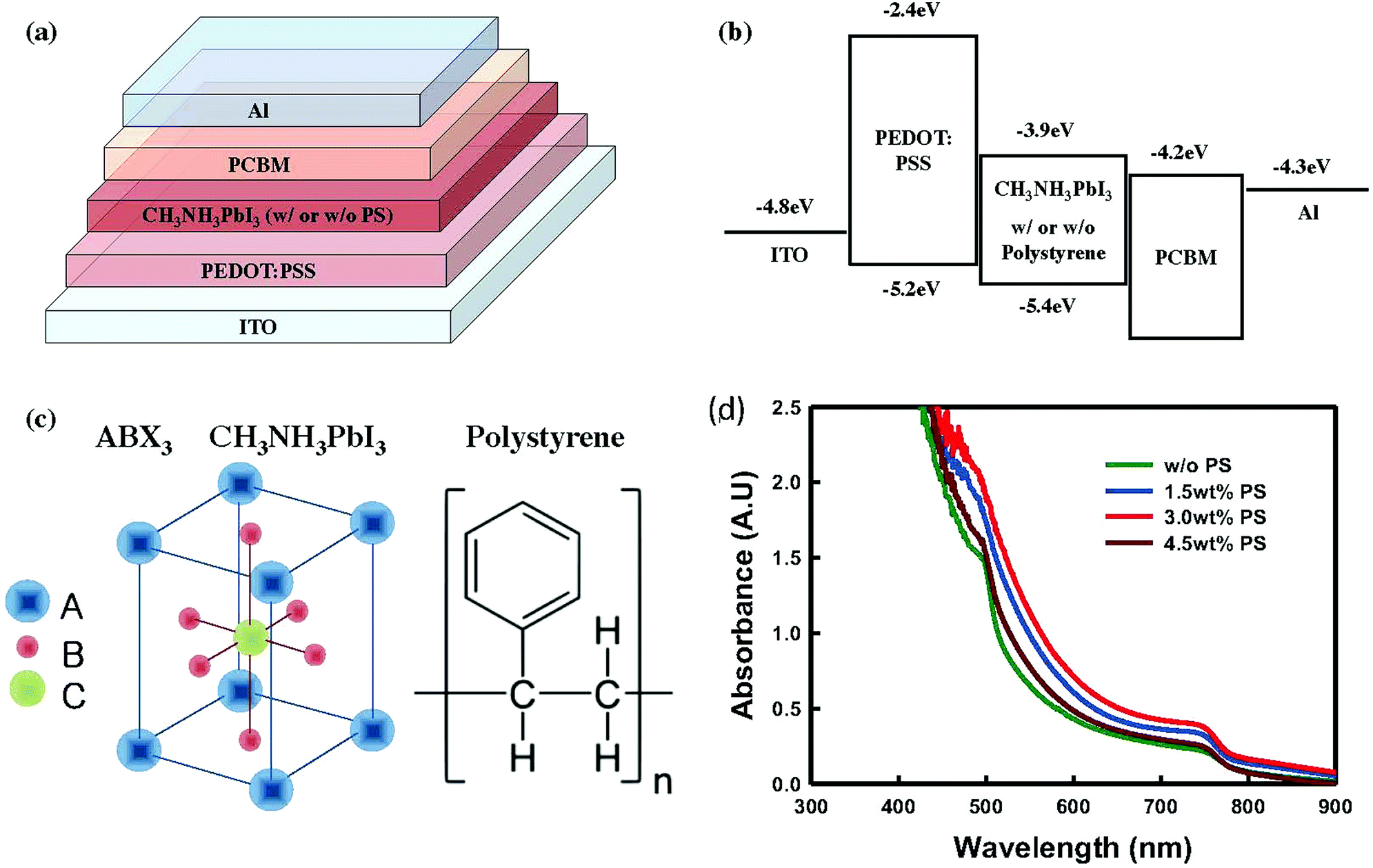 | ||
| Fig. 1 Device structure and energy level diagrams of a complete perovskite solar cell, and material properties. (a) Schematic design of a complete perovskite solar cell (ITO/PEDOT:PSS/CH3NH3PbI3 (with or without polystyrene (PS))/PC60BM/Al), (b) diagram of the energy levels of each layer in the device, (c) molecular structure of CH3NH3PbI3 (ABX3) and PS, and (d) UV-visible absorbance of the perovskite films spin-coated on glass with and without PS (0.5, 1.0, 1.5, 3.0, 4.5, 6.0 wt%); the processing conditions are similar to those used to fabricate the conventional perovskite solar cells. The energy level for each layer has been taken from ref. 31b. | ||
Bazan et al. previously reported that inserting a high-molecular-weight PS (2 × 10⁷ M) could increase the organic photovoltaic (OPV) performance by favoring the crystallization of p-DTS(FBTTh2)2, and enhancing the phase separation.32 Motivated by this finding, we aim at understanding if the PS can have a similar role in the crystallization of the perovskite absorber layer and device performance.
Prior to the film deposition, the PS is blended into the CH3NH3PbI3 precursor solution. Current density–voltage (J–V) plots under one sun, and external quantum efficiency (EQE) spectra are depicted in Fig. 2a and b, respectively. Solar cell parameters are listed in Table 1. Due to the low crystallinity of the pristine perovskite film along with the tiny crystallite size, the fabricated cell without PS exhibited an average device performance with a short-circuit current density (JSC) of 17.2 mA cm−2, an open-circuit voltage (VOC) of 0.96 V, a fill factor (FF) of 69.7% and a PCE of 11.7%. We investigated different loadings of PS ranging from 0.5 to 4.5% of the total absorber material mass in the precursor perovskite solution. Here, the thickness of the absorber layers was fixed at ∼300 nm to allow direct comparison with a perovskite system of the same dimensions. As illustrated in Table 1 and Fig. 2, incorporation of 1.5 wt% PS enhanced both JSC and FF, leading to a PCE improvement of about 13%, which is a positive impression in view of the integration of an insulating component into the perovskite precursor solution. Approximately ∼10% improvement in JSC is observed. This superior performance of the device incorporating the insulating PS is in agreement with the previously demonstrated work.32 Moreover, by incorporating 1.5% PS into the perovskite system, a decrease of 1 order of magnitude in the leakage is detected (Fig. S1†). With the increase of PS amount from 1.5 wt% to 3.0 wt%, further improvement of conversion efficiency was found with the average device exhibiting a PCE of 13.3% with a JSC of 19.2 mA cm−2, a VOC of 0.95 V, and a FF of 71.8%. The increase of photocurrent density is possibly associated with the increased absorption as shown in Fig. 1d. Moreover, plots of JSC as a function of PS composition for all four systems discussed here can be found in Fig. S2,† with current improving steadily with increase in the amount of PS before it plunges as the amount exceeds a certain threshold. The significant enhancement can be ascribed to the reduced pinholes resulting from improved crystallinity with preferred orientation, and larger grain size, which subsequently enhanced charge dissociation and transport due to suppressed defect-assisted charge recombination, as we will demonstrate in the following. On further increase of the content of PS exceeding 3.0 wt%, the solar cell parameter namely PCE drastically decreased to 10.8% along with a JSC of 15 mA cm−2, a VOC of 0.97 V, and a FF of 73.5%. The poor performance with PCE of 10.8% can be attributed to the comparable leakage current (with the cell without PS). The external quantum efficiency (EQE) shown in Fig. 2b verifies the improved JSC of the fabricated devices, in which the integral photocurrent densities deduced from EQE plots are consistent with the experimental values (see Table 1). To ensure the reproducibility and validity of our data, we have fabricated 48 samples of which 56% reached PCE over 12% (Fig. S3†).
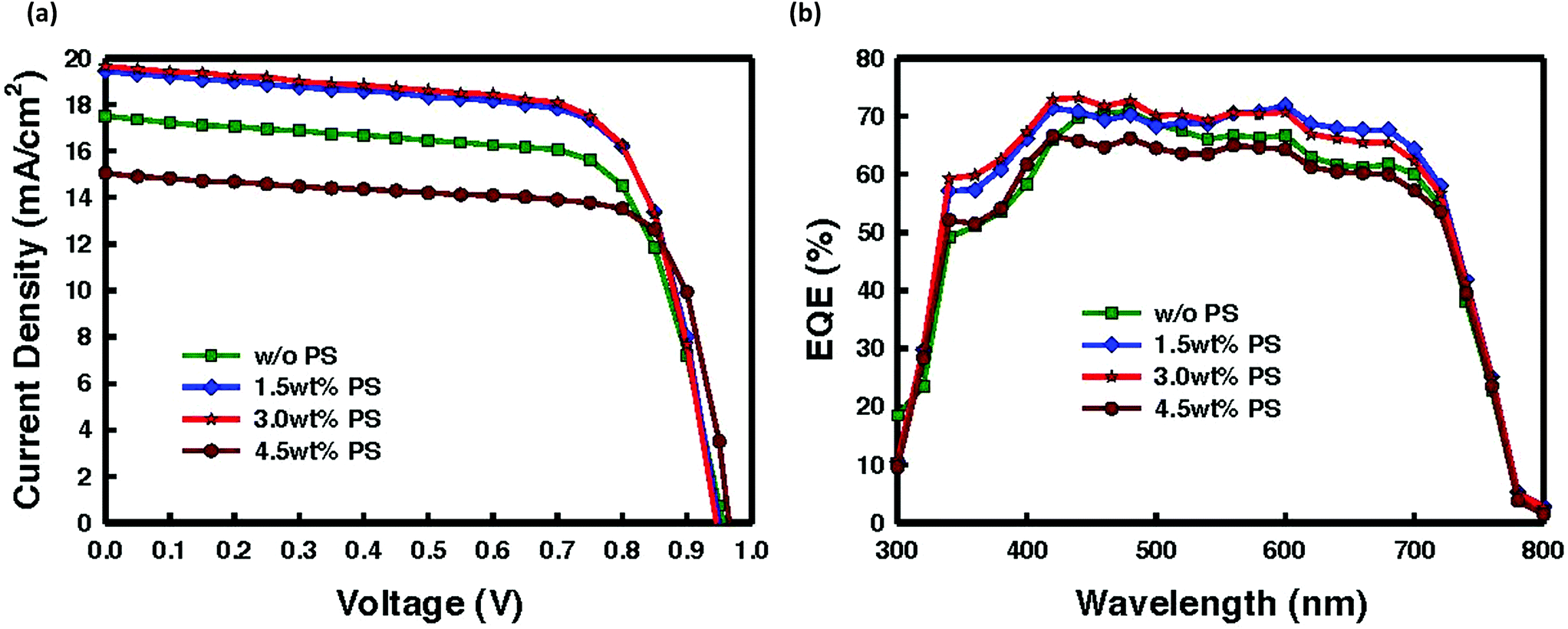 | ||
| Fig. 2 Device performance of perovskite solar cells with different concentrations of polystyrene (ITO/PEDOT:PSS/CH3NH3PbI3 (without or with 1.5, 3.0, 4.5 wt% PS)/PC60BM/Al). (a) J–V characteristics under one sun condition (100 mW cm−2, AM1.5G) and (b) external quantum efficiency (EQE) spectra of perovskite solar cells. | ||
| Polystyrene concentration (wt%) | J SC (mA cm−2) | V OC (V) | FF (%) | PCE (%) | HI |
|---|---|---|---|---|---|
| 0 | 17.2 ± 0.44 | 0.96 ± 0.05 | 69.4 ± 2.2 | 11.7 ± 0.41 | 0.03 |
| 1.5 | 19.0 ± 0.42 | 0.95 ± 0.05 | 70.7 ± 2.6 | 13.0 ± 0.43 | 0.005 |
| 3.0 | 19.2 ± 0.40 | 0.95 ± 0.04 | 71.8 ± 2.3 | 13.3 ± 0.39 | 0 |
| 4.5 | 15.0 ± 0.41 | 0.97 ± 0.05 | 73.5 ± 2.0 | 10.8 ± 0.46 | 0.01 |
We attribute the decrease in leakage current to the presence of PS in the perovskite system, which seems to improve the perovskite film properties remarkably. To verify this assumption, we analyzed the dewetting properties in all cases, where a remarkable number of dewetting points were observed on the absorber layer deposited onto the PEDOT:PSS layer. The number of dewetting points slightly reduced upon loading of 1.5 wt% PS into the perovskite precursor solution. A notable feature was observed during the integration of 3.0 wt% PS, where the number of dewetting points is reduced by more than half compared to the pristine perovskite solution. A decrease in dewetting points results in a homogeneous film featuring larger grain size and defect-free morphology (Fig. 4c). However, further increment of the proportion of PS up to 4.5 wt% results in a slight increment of dewetting points, which one could associate with the larger and merged grain size, which unfortunately results in a decrease in the device performance. Concerning the effect of PS on the viscosity of the solution, no significant changes were observed. Thus, one can clearly conclude that the solution undergoes wetting very well.
Next we conducted atomic force microscopy (AFM) measurements to verify the root-mean-square (RMS) roughness and the average peak valley roughness (PV) (Table 2). As can be seen from the images, the root-mean-square (RMS) roughness for pristine perovskite is around 10.4 nm with the peak-to-valley roughness (PV) being approximately 106 nm, which is relatively small compared to those in other solution processed perovskite films.33 However, the film has a small crystallite size with an average size of 200 nm (Fig. 4a), which will inevitably increase grain boundary density and limit device performance. Further decrement in the RMS and PV roughness was found upon the incorporation of 3.0 wt% of PS into the perovskite precursor solution, where the RMS and PV roughness were 9.28 nm and 77 nm, respectively. It is worth noting that there is a lack of pinholes for 3.0 wt% PS-derived thin film as compared with films of pristine CH3NH3PbI3 and 1.5 wt% PS. However, when the threshold amount of PS loading exceeded 3.0%, these values undesirably increased again, even surpassing the value of pristine perovskite. Larger pinholes were detected with 4.5 wt% PS incorporation into the perovskite precursor solution, resulting in decreased surface coverage, which caused leakage current (Fig. S1†). The significant increase of RMS roughness for 4.5 wt% PS can be attributed to the large pinholes. These findings are consistent with the values obtained from conductive AFM (Fig. 3a–d right panels). These observations indicate that an optimum PS amount is required to demonstrate lower roughness. However, excessive amount of PS leads to significantly higher RMS roughness and PV roughness, which subsequently influence the device performance. These observations also show that a decrease in the surface roughness results in a decrease in the number and size of dewetting points. It is safe to conclude that an optimum amount of PS is required to generate large grain size with lower RMS roughness. Even though the grain size further increased for 4.5 wt% PS, the RMS roughness significantly increased.
| Polystyrene concentration (wt%) | Roughness | Dewetting points of the absorber layer | ||||
|---|---|---|---|---|---|---|
| R q (nm) | R p–v (nm) | C max (pA) | Number of points (mm−2) | Area (μm2) | Fractional area (%) | |
| w/o PS | 10.41 | 106.19 | 39.06 | 20 | 105 | 0.22 |
| 1.5 | 10.28 | 81.80 | 42.42 | 15 | 100 | 0.12 |
| 3.0 | 9.28 | 77.06 | 43.64 | 6 | 107 | 0.24 |
| 4.5 | 14.16 | 115.63 | 34.46 | 9 | 102 | 0.14 |
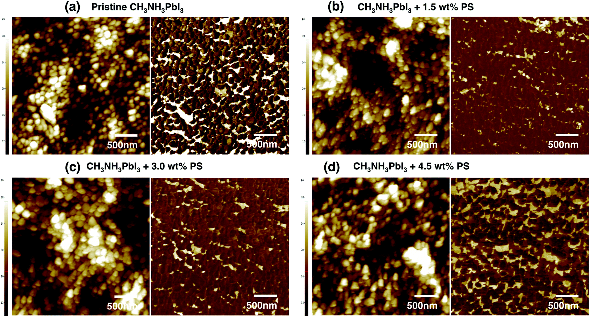 | ||
| Fig. 3 Surface properties of thin films used in this work. The (a–d left panels) atomic force microscopy (AFM) and (a–d right panels) conductive AFM (cAFM) images of CH3NH3PbI3 perovskite thin film with different concentrations of polystyrene on the ITO/PEDOT:PSS layer. | ||
A series of conducting AFM measurements provide additional information on the electronic properties (conducting paths along grains and grain boundaries) of the perovskite thin film. We performed the cAFM measurements under high vacuum and dark conditions to avoid any influences from light and moisture with a constant voltage of 0.5 V applied to the CH3NH3PbI3 perovskite thin films via a conducting Pt–Ir-coated AFM tip. In the cAFM measurements, the measured current is related to the conductivity of the perovskite thin films between the AFM tip and the substrate. If the bias is negative, the very small current that transports through the perovskite thin film can be measured regardless of whether the illumination is applied or not. This is due to the one-way transport property of CH3NH3PbI3 owing to the presence of the electron-blocking PEDOT:PSS layer. Meanwhile, the current can be measured when a positive bias is applied. The current increases as the bias increases. It is worth noticing that the obtained current under illumination is remarkably higher compared to the current under dark conditions. This is because the illumination facilitates a considerable conductivity improvement by generating copious charges. The current maps (Fig. 3a–d right panels) demonstrate an inhomogeneous distribution of differently conducting regimes. Even though the maximum current of the pristine perovskite thin film was lower compared to that of perovskite with 1.5 wt%, and 3.0 wt% loaded PS, still the pristine perovskite thin film illustrates conducting paths along grain boundaries. The perovskite precursor solution incorporated with 1.5 wt% PS featuring an average grain size of approximately 300 to 400 nm produced a current of 42.42 pA. The striking increase in the maximum current can be attributed to the surface with fewer pinholes, along with larger grain size compared to the pristine perovskite thin film.
The maximum current value increased to 43.64 pA upon loading the perovskite precursor solution with 3.0 wt% PS. The enhancement in the maximum current can be attributed to the large grain size, almost pinhole-free morphology, and high quality crystallite morphology. However, the maximum current decreased notably upon incorporating 4.5 wt% PS. This is due to the fact that the thin film demonstrated larger pinholes and less homogeneous morphology. The decreased maximum current also contributed to the total leakage current in the fabricated perovskite device with 4.5 wt% PS. The observed results indicate that the electrical conductivity of perovskite loaded PS increased with the amount of PS. This could be ascribed to the JSC improvement achieved for the fabricated devices. We further verify our observations with XRD measurements (discussed below). The cAFM observations also indicate inhomogeneous current spots associated with the deposited thin film's nanostructure being influenced by the film's composition as a result of a stoichiometry-affected nucleation and crystallization behavior. From cAFM measurements, we conclude that the perovskite precursor solution loaded with PS is more conductive than pristine perovskite solution.
It is common knowledge that the performance of perovskite solar cells is related to the crystallinity of the deposited perovskite thin film. This is due to the fact that defects in the perovskite layer eventually cause shorts, and charge carrier trapping and recombination sites. Furthermore, charge dissociation efficiency, charge transport, and diffusion length are greatly influenced by the crystallinity and crystal size.12,21Fig. 4 presents the scanning electron microscopy (SEM) images to examine the influence of PS on the perovskite system with perovskite thin films of different PS loadings. One can see that pristine perovskite demonstrates smaller grain size <200 nm with obvious pinholes distributed throughout the surface. Upon incorporating 1.5 wt% PS, the grain size becomes bigger (between 300 and 400 nm) with better surface coverage and less roughness. More regular crystallite morphology with fewer pinholes can be observed in Fig. 4c upon addition of 3.0 wt% PS to the perovskite precursor solution. The optimized loading of PS in the perovskite precursor solution was found to be 3.0 wt%, which provides us with the high JSC (19.2 mA cm−2) and FF (71.8%). The high JSC and FF indicate the effective light harvesting of the perovskite absorber layer as well as efficient charge extraction and transport, respectively. Despite some positive influences utilizing PS in the perovskite precursor, it also offers a negative effect on charge separation, which might contribute to the reduction in photocurrent generation at higher loading (4.5 wt%). Exceeding the threshold loading of PS prepared from 4.5 wt% PS (Fig. 4d) depicted a huge grain size (>1000 nm) with less surface coverage, and fewer crystallites compared to that of the surface topography in Fig. 4c.
 | ||
| Fig. 4 Structural properties of thin films used in this work. Top-view SEM images of (a–d) CH3NH3PbI3 perovskite films with different concentrations of polystyrene deposited on the ITO/PEDOT:PSS layer. The CH3NH3PbI3 grain size proportionally increased (200 nm → 1.1 μm) with increase in the concentration of polystyrene. The cross-sectional SEM images of (e–h) CH3NH3PbI3 perovskite films with different concentrations of polystyrene deposited on the ITO/PEDOT:PSS substrate. | ||
In addition to the top view SEM, Fig. 4e–h demonstrate cross-sectional SEM for all four cases, where one can clearly see that the incorporation of 3.0 wt% of PS leads to desirable continuous morphology. One can also see that loading perovskite precursor solution with 4.5 wt% PS not only enlarged the grain size but also produced an uneven perovskite thin film. Several big “humps” can be found on the film deposited onto the PEDOT:PSS layer.
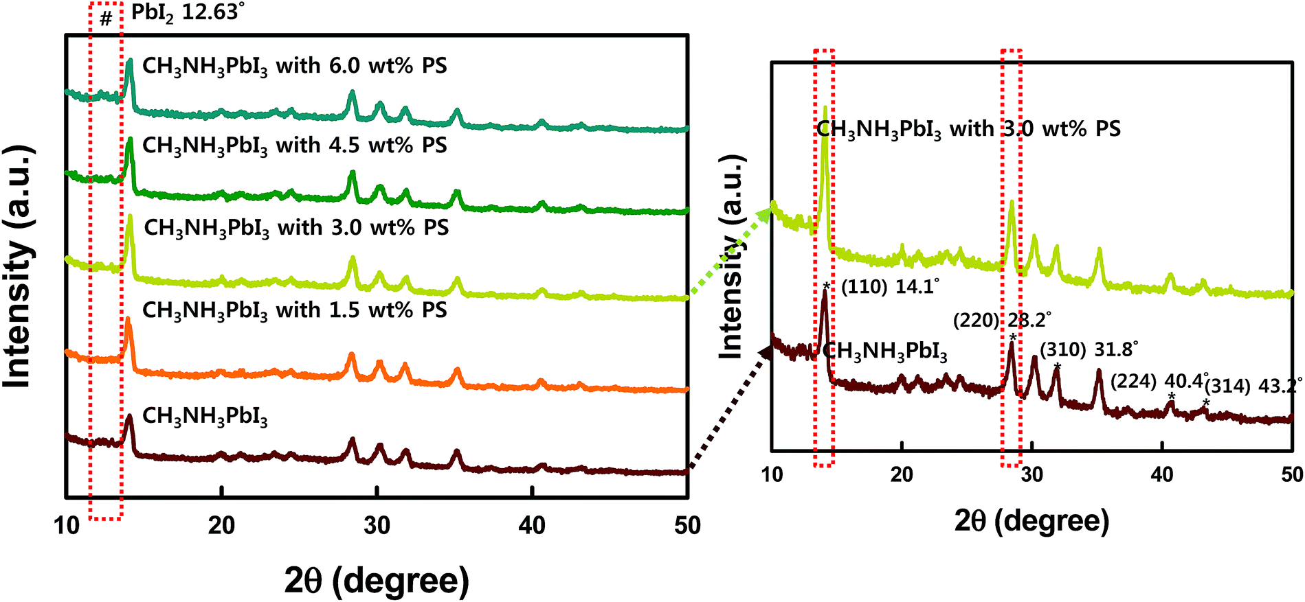
The improved crystallization of CH3NH3PbI3 by PS is also verified by X-ray diffraction patterns as shown in Fig. 5 (right panel). From the absorption spectra it is observed that the perovskite precursor solution with 3.0 wt% of PS demonstrates enhanced light absorption across the visible regime. This trend is in agreement with the observed EQE spectra (Fig. 2b). Further verification of the improved crystallinity of CH3NH3PbI3 loaded with 3.0 wt% PS can be done from the XRD patterns depicted in Fig. 5 (right panel), where one sees the improved intensity peaks centered at 14.1° and 28.2°. The scattering peaks at 14.1° and 28.2° can be indexed to the (110) and (220) crystal planes of the tetragonal lattice of the CH3NH3PbI3 perovskite, respectively.8 On a closer look, the closely stacked XRD diffraction patterns demonstrated in Fig. S4† also confirmed the intense peaks at 14.1° and 28.2°after PS incorporation. The integration of PS greatly favors the preferential crystal growth along (110) and (220) directions, resulting in improved crystallinity of the perovskite film.
 | ||
| Fig. 5 XRD diffraction patterns of CH3NH3PbI3 thin films spin-coated on glass with and without PS (1.5, 3.0, 4.5, and 6.0 wt%). | ||
We further characterized the film derived from different loadings of PS by XRD diffraction patterns as shown in Fig. 5 (left panel). In the pristine perovskite thin film, smaller grain size with random crystal orientation is found because of the fast crystallization of the precursor film. Upon solvent annealing, faster grain growth and merging of grains were found (Fig. 5 red (without PS) and blue panels (with 6 wt% PS)). In the XRD patterns red and blue panels illustrate the rapid diffraction intensities of (100) and (220) peaks during this process, suggesting the grain growth with preferred orientation. Further loading with 4.5 wt% PS dramatically changes the surface morphology (Fig. 3d, and 4d and h), which corresponds to the device performance. Finally, the observation of enhanced crystallization from XRD patterns in the perovskite loaded with PS is in accordance with the absorbance spectra, SEM and AFM images, and J–V curves.
The effect of the introduction of PS in the perovskite device is further monitored by time resolved photoluminescence (PL). The PL is monitored at 770 nm upon excitation at 460 nm in the first 40 ns temporal window. Fig. 6 shows the PL decay for all four cases. For the perovskite thin film without PS, the PL shows fast and slow decay components with lifetimes of 1.44 ± 0.06 ns and 13.80 ± 0.21 ns, respectively. The weight fractions derived from the exponential fitting are 81% and 19%, respectively. Since the perovskite film is deposited on the PEDOT:PSS substrate the fast component might be related to charge transfer to the substrate while the long living one, extending out of our temporal window, is what is usually observed.9b,9c Note that in the fluence regime used, a charge density of approximately 1017 is created. At this excitation density, traps are filled and the emission is mainly due to band to band charge recombination. The integration of 1.5 wt% PS in the perovskite precursor solution slightly increases the fast decay lifetime to 1.60 ± 0.04 ns while improving the weight fraction to 85%.
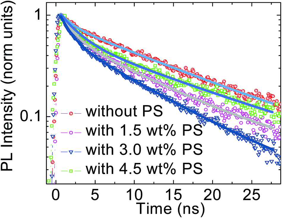 | ||
| Fig. 6 The time resolved PL demonstrates the reduced exciton quenching lifetime without PS and with 1.5 wt%, 3.0 wt%, and 4.5 wt% PS. | ||
In the perovskite solution with 3.0 wt% of PS the fast decay lifetime reduces to 1.42 ± 0.02 ns before increasing back to 2.36 ± 0.07 ns upon incorporating 4.5 wt% PS. This suggests a slight improvement of charge transfer to the PEDOT:PSS/perovskite interface. This can be due to the better interfacial contact and improved film morphology. This value also supports our early findings that the high JSC and FF in the device constructed with 3.0 wt% PS can be attributed to the improved charge injection and collection due to the better morphology and crystal quality of the perovskite matrix. However, the decrease in weight fraction value from 90% to 83% upon 4.5 wt% PS loading corresponds to ineffective charge dissociation and transport to the PEDOT:PSS and PC60BM layers.
However, we cannot exclude that PS can partially fill shallow trap defects, too. To date, the hysteresis between forward and reverse J–V scans is attributed to the slow response time of the cell to a change in load, and the mechanism, although yet to be well understood, has been discussed in recent studies.34,35Fig. 7 shows the hysteresis behavior for our fabricated perovskite solar cells with and without PS. Among all systems, the constructed device without PS demonstrated severe hysteresis characteristics. Meanwhile, Fig. 7c shows the J–V curves for the best constructed devices loaded in 3.0 wt% PS measured under AM1.5G (100 mW cm−2) solar illumination in air, exhibiting superior performance with JSC = 19.20 mA cm−2, VOC = 0.95 V, FF = 71.80% and PCE = 13.30% when scanned from forward bias to short circuit, and JSC = 18.47 mA cm−2, VOC = 0.90 V, FF = 76.02% and PCE = 12.64% when scanned from short circuit to forward bias.
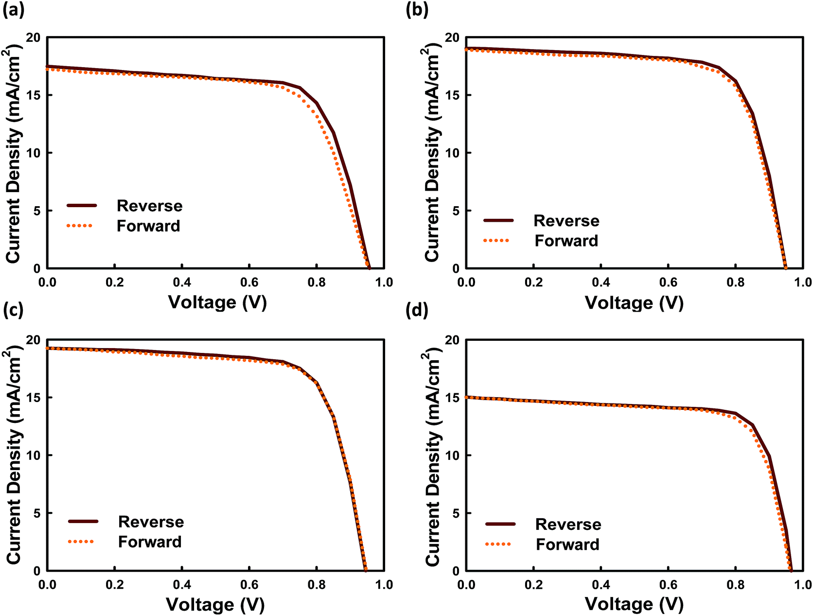 | ||
| Fig. 7 J–V plots for perovskite solar cells (a) without PS, (b) with 1.5 wt% PS, (c) with 3.0 wt% PS, and (d) with 4.5 wt% PS under one sun conditions (100 mW cm−2, AM1.5G). The scan rate for both scans is 10 mV s−1. | ||
We found that the current hysteresis becomes more obvious as the grain size decreases. For the 200 nm grains current remains unchanged; however, the FF at RS is lower compared with the FS case. Relatively little difference in FF between FS and RS is demonstrated, even for a slight increase in size from 600 nm to 1000 nm. Because the prominent feature in the J–V hysteresis appears near open-circuit conditions, a modified J–V hysteresis index36 is defined by eqn (1):
| HI = JRS(0.8VOC) − JFS(0.8VOC)/JRS(0.8VOC), | (1) |
The air stability of MAPbI3 solar cells fabricated without PS and with 1.5 wt% PS, 3.0 wt% PS, and 4.5 wt% PS as a function of storage time in air under ambient conditions is demonstrated in Fig. 8. The encapsulated perovskite solar cells based on 3.0 wt% PS illustrate remarkably better air stability. The conversion efficiency remains above 80% of the original value even after storage in air for 60 days, compared to the conversion efficiency of the perovskite device without PS which deteriorated by almost 30% after air exposure for 60 days. A notable feature is that all devices incorporated with PS maintained their PCE above 80% after 60 days of exposure. The stability of devices with PS stems from the insulating properties of PS against oxygen and moisture, which reduces the decomposition probability of MAPbI3 perovskite films. From this point of view, the integration of PS in perovskite precursor solution results in significant improvement in air stability. It should be noted that improved stability has also been previously demonstrated by Zhang et al.,28 by inserting an ultrathin Al2O3 layer at the ZnO/perovskite interface. They achieved a slightly higher device performance compared to our work due to the difference in device architecture and the main difference could be due to the fact that we have incorporated PS into the perovskite layer while they inserted an Al2O3 layer in between ZnO and perovskite.
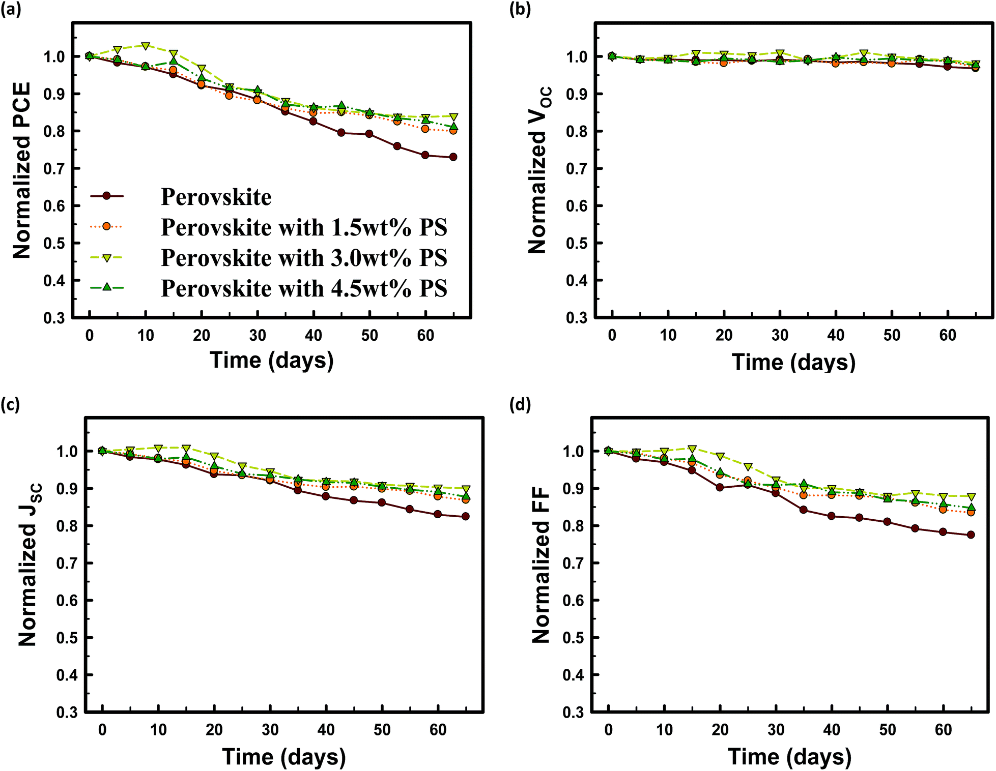 | ||
| Fig. 8 Stability of the devices in an ambient environment. Device performances of ITO/PEDOT:PSS/perovskite/PCBM/Al (brown), ITO/PEDOT:PSS/perovskite with 1.5 wt% PS/PCBM/Al (orange), ITO/PEDOT:PSS/perovskite with 3.0 wt% PS/PCBM/Al (emerald) and ITO/PEDOT:PSS/perovskite with 4.5 wt% PS/PCBM/Al (green) structures as a function of storage time in an ambient environment (30–50% humidity, T = 25 °C). (a) Normalized PCE, (b) normalized VOC, (c) normalized JSC and (d) normalized FF. | ||
Conclusion
In summary, we have presented a notably improved PCE (∼13.7%) of planar-heterojunction perovskite solar cells from 11.7% up to 13.3% by integrating 3.0 wt% insulating polystyrene into the perovskite precursor solutions to enhance the crystallization of perovskite thin films. We demonstrated that integrating polystyrene facilitates uniform nucleation, as verified by SEM and AFM images, and absorbance and XRD spectra. The improved crystallization facilitates efficient charge transfer between the active interface and the perovskite layer. Subsequently, a moderate PCE was obtained from the device fabricated by the sub-100 °C solution process. We envisage that other device configurations may benefit from this approach in so far as film thickness control is concerned.Conflicts of interest
There are no conflicts to declare.Acknowledgements
H. P. K, A. R. B. M. Y. and J. J. would like to thank MOTIE (Ministry of Trade, Industry & Energy (10052044)) and KDRC (Korea Display Research Corporation) support program for the development of future device technology for the display industry.References
- K. Liang, D. B. Mitzi and M. T. Prikas, Chem. Mater., 1998, 10, 403 CrossRef CAS.
- A. Kojima, K. Teshima, Y. Shirai and T. Miyasaka, J. Am. Chem. Soc., 2009, 131, 6050 CrossRef CAS PubMed.
- J. H. Im, C. R. Lee, J. W. Lee, S. W. Park and N. G. Park, Nanoscale, 2011, 3, 4088 RSC.
- L. Etgar, P. Gao, Z. Xue, Q. Peng, A. K. Chandiran, B. Liu, M. K. Nazeeruddin and M. Grätzel, J. Am. Chem. Soc., 2012, 134, 17396 CrossRef CAS PubMed.
- M. M. Lee, J. Teuscher, T. Miyasaka, T. N. Murakami and H. J. Snaith, Science, 2012, 338, 643 CrossRef CAS PubMed.
- H. S. Kim, C. R. Lee, J. H. Im, K. B. Lee, T. Moehl, A. Marchioro, S. J. Moon, R. Humphry-Baker, J. H. Yum, J. E. Moser, M. Grätzel and N. G. Park, Sci. Rep., 2012, 2, 1 Search PubMed.
- J. H. Noh, S. H. Im, J. H. Heo, T. N. Mandal and S. I. Seok, Nano Lett., 2013, 13, 1764 CrossRef CAS PubMed.
- J. H. Heo, S. H. Im, J. H. Noh, T. N. Mandal, C. S. Lim, J. A. Chang, Y. H. Lee, H. Kim, A. Sarkar, M. K. Nazeeruddin, M. Grätzel and S. I. Seok, Nat. Photon., 2013, 7, 486 CrossRef CAS.
- (a) J. Burschka, N. Pellet, S. J. Moon, R. Humphry-Baker, P. Gao, M. K. Nazeeruddin and M. Grätzel, Nature, 2013, 499, 316 CrossRef CAS PubMed; (b) C. Roldan-Carmona, P. Gratia, I. Zimmermann, G. Grancini, P. Gao, M. Grätzel and M. K. Nazeeruddin, Energy Environ. Sci., 2015, 8, 3550 RSC; (c) E. Mosconi, G. Grancini, C. Roldan-Carmona, P. Gratia, I. Zimmermann, M. K. Nazeeruddin and F. De Angelis, Chem. Mater., 2016, 28, 3612 CrossRef CAS.
- M. Liu, M. B. Johnston and H. J. Snaith, Nature, 2013, 501, 395 CrossRef CAS PubMed.
- S. Ryu, J. H. Noh, N. J. Jeon, Y. C. Kim, W. S. Yang, J. Seo and S. I. Seok, Energy Environ. Sci., 2014, 7, 2614 RSC.
- G. Xing, N. Mathews, S. Sun, S. S. Lim, Y. M. Lam, M. Grätzel, S. Mhaisalkar and T. C. Sum, Science, 2013, 342, 344 CrossRef CAS PubMed.
- N. J. Jeon, H. G. Lee, Y. C. Kim, J. Seo, J. H. Noh, J. Lee and S. I. Seok, J. Am. Chem. Soc., 2014, 136, 7837 CrossRef CAS PubMed.
- G. E. Eperon, S. D. Stranks, C. Menelaou, M. B. Johnston, L. M. Herz and H. J. Snaith, Energy Environ. Sci., 2014, 7, 982 RSC.
- J. Y. Jeng, Y. F. Chiang, M. H. Lee, S. R. Peng, T. F. Guo, P. Chen and C. Wen, Adv. Mater., 2013, 25, 3727 CrossRef CAS PubMed.
- G. E. Eperon, V. M. Burlakov, P. Docampo, A. Goriely and H. J. Snaith, Adv. Funct. Mater., 2013, 24, 151 CrossRef.
- P. Docampo, J. M. Ball, M. Darwich, G. E. Eperon and H. J. Snaith, Nat. Commun., 2013, 4, 2761 CrossRef PubMed.
- (a) B. Conings, L. Baeten, C. D. Dobbelaere, J. D'Haen, J. Manca and G. Boyen, Adv. Mater., 2014, 26, 2042 CrossRef PubMed; (b) S. PAek, P. Schouwink, E. Nefeli Athanasopolou, K. T. Cho, G. Grancini, Y. Lee, Y. Zhang, F. Stellacci, M. K. Nazeeruddin and P. Gao, Chem. Mater., 2017, 29, 3490 CrossRef CAS.
- A. Abrusci, S. D. Stranks, P. Docampo, H. L. Yip, A. K. Y. Jen and J. Snaith, Nano Lett., 2013, 13, 3124 CrossRef CAS PubMed.
- J. M. Ball, M. M. Lee, A. Hey and H. Snaith, Energy Environ. Sci., 2013, 6, 1739 RSC.
- G. E. Eperon, V. M. Burlakov, P. Docampo, A. Goriely and H. J. Snaith, Adv. Funct. Mater., 2013, 24, 151 CrossRef.
- M. Li, Z.-K. Wang, M.-P. Zhuo, Y. Hu, K.-H. Hu, Q.-Q. Ye, S. M. Jain, Y.-G. Yang, X.-Y. Gao and L.-S. Liao, Adv. Mater., 2018, 30, 1800258 CrossRef PubMed.
- L.-L. Jiang, Z.-K. Wang, M. Li, C.-C. Zhang, Q.-Q. Ye, K.-H. Hu, D.-Z. Lu, P.-F. Fang and L.-S. Laio, Adv. Funct. Mater., 2018, 28, 1705875 CrossRef.
- Z.-K. Wang, M. Li, Y.-G. Yang, Y. Hu, H. Ma, X.-Y. Gao and L.-S. Liao, Adv. Mater., 2016, 28, 6695 CrossRef CAS PubMed.
- C.-C. Zhang, M. Li, Z.-K. Wang, Y.-R. Jiang, H.-R. Liu, Y.-G. Yang, X.-Y. Gao and H. Ma, J. Mater. Chem. A, 2017, 5, 2572 RSC.
- M. Li, Y. H. Chao, T. Kang, Z.-K. Wang, Y.-G. Yang, S.-L. Feng, Y. Hu, X.-Y. Gao, L. S. Liao and C.-S. Hsu, J. Mater. Chem. A, 2016, 4, 15088 RSC.
- X. Gong, M. Li, X.-B. Shi, Z.-K. Wang and L.-S. Liao, Adv. Funct. Mater., 2015, 25, 6671 CrossRef CAS.
- H. Si, Q. Liao, Z. Zhang, Y. Li, X. Yang, G. Zhang, Z. Kang and Y. Zhang, Nano Energy, 2016, 22, 223 CrossRef CAS.
- H. Si, Q. Liao, Z. Kang, Y. Ou, J. Meng, Y. Liu, Z. Zhang and Y. Zhang, Adv. Funct. Mater., 2017, 30, 1701804 CrossRef.
- D. Bi, C. Yi, J. Luo, J.-D. Decoppet, F. Zhang, S. M. Zakeeruddin, X. Li, A. Hagfeldt and M. Gratzel, Nat. Energy, 2016, 1, 16142 CrossRef CAS.
- (a) Y. Huang, W. Wen, S. Mukherjee, H. Ade, E. J. Kramer and G. C. Bazan, Adv. Mater., 2014, 26, 4168 CrossRef CAS PubMed; (b) J. You, Z. Hong, Y. Yang, Q. Chen, M. Cai, T.-B. Song, C.-C. Chen, S. Lu, Y. Liu, H. Zhou and Y. Yang, ACS Nano, 2015, 8, 1674 CrossRef PubMed.
- Y. Huang, W. Wen, S. Mukherjee, H. Ade, E. J. Kramer and G. C. Bazan, Adv. Mater., 2014, 26, 4168 CrossRef CAS PubMed.
- E. L. Unger, E. T. Hoke, C. D. Bailie, W. H. Nguyen, A. R. Bowring, H. Heumüller, M. G. Christoforo and M. D. McGehee, Energy Environ. Sci., 2014, 7, 3690 RSC.
- Q. Chen, H. Zhou, Z. Hong, S. Luo, H. S. Duan, H. H. Wang, Y. Liu, G. Li and Y. Yang, J. Am. Chem. Soc., 2014, 136, 622 CrossRef CAS PubMed.
- W. Zhang, M. Saliba, D. T. Moore, S. K. Pathak, M. T. Hörantner, T. Stergiopoulos, S. D. Stranks, G. E. Epron, J. A. A. Webber, A. Abate, A. Sadhanala, S. Yao, Y. Chen, R. H. Friend, L. A. Estroff, U. Wiesner and H. J. Snaith, Nat. Commun., 2015, 6, 6142 CrossRef CAS PubMed.
- H. S. Kim and N. G. Park, J. Phys. Chem. Lett., 2014, 5, 2927 CrossRef CAS PubMed.
Footnote |
| † Electronic supplementary information (ESI) available. See DOI: 10.1039/c8na00052b |
| This journal is © The Royal Society of Chemistry 2019 |