
Seamless interconnections of sp2-bonded carbon nanostructures via the crystallization of a bridging amorphous carbon joint†
Longze
Zhao‡
,
Yong
Cheng‡
,
Qiaobao
Zhang
 and
Ming-Sheng
Wang
*
and
Ming-Sheng
Wang
*
Department of Materials Science and Engineering, College of Materials, and Pen-Tung Sah Institute of Micro-Nano Science and Technology, Xiamen University, Xiamen, Fujian 361005, China. E-mail: mswang@xmu.edu.cn
First published on 9th October 2018
Abstract
Two multiwalled carbon nanotubes (MWNTs) were seamlessly connected via the crystallization of a bridging amorphous carbon (a-C) joint using a transmission electron microscope. Technically, such a CNT connection involves electron beam induced deposition of amorphous carbon at the gap between the two nanotubes, followed by a controlled Joule heating process. Upon heating, the deposited a-C crystalized into a multi-layer tubular structure that merges into open-ended CNT shells, forming continuous graphitic layers across the junction. For the first time, seamless repairing of a pure MWNT after its electrical breakdown is thus achieved, accompanied by the nearly full recovery of its electrical conductance. More generally, we demonstrated its usage in the seamless joining of any two nanotubes, regardless of their difference in diameter, chirality, shell number and axis orientation. Molecular dynamics calculations reveal more details on how the a-C joint evolves into coherent sp2-bonded networks connecting the given nanotube pairs, thus highlighting the unique ability of the C system to reconstruct itself into any required sp2 graphitic configuration at high temperature. This seamless-joining method can be further extended to the connection between nanotubes and graphene, exhibiting its particular technological importance for building novel sp2 carbon-based nanostructures and devices via the bottom-up approach.
Conceptual insightsJoining of materials at the nanoscale is critical for building complicated nanostructures or devices via the bottom-up approach, and it is particularly true for sp2 carbon technologies. Carbon systems have the unique ability to evolve from amorphous phases into various coherent sp2 structures by different C–C bond reconstruction at elevated temperatures. In this work, we present a novel CNT-joining technique via the crystallization of an amorphous carbon (a-C) deposit bridging the gap between two CNTs, which enables the seamless connection between any two MWNTs with open-ended shells, as demonstrated herein by in situ TEM. Upon Joule heating, the deposited a-C crystalizes into a multi-layer tubular structure that merges into open-ended CNT shells, forming continuous graphitic layers across the junction. Repairing of a pure MWNT in a seamless manner after its electrical breakdown is thus achieved for the first time. More generally, we demonstrate its feasibility in the seamless joining of any two MWNTs, regardless of their difference in diameter, chirality, shell number and axis orientation. Molecular dynamics simulations reveal more details on how the a-C joint evolves into coherent networks containing non-six-membered rings so as to connect the given nanotube pairs with complex geometries and different structures, verifying the high flexibility of sp2 bonds to form any required coherent configurations. We further demonstrate the seamless joining process between individual CNTs and graphene sheets. The developed seamless-joining method is envisaged to be practically valuable in a variety of device applications, from CNT repairing and interconnecting in nanocircuits, to the building of all-sp2 carbon systems. |
Introduction
Joining of materials at the nanoscale is critical for building complicated nanostructures or devices via the bottom-up approach.1–5 A well-known example is the constant pursuit of nanowelding techniques over the past few decades to realize better connection of individual carbon nanotubes (CNTs).6–16 CNTs hold great potential as building blocks for constructing, e.g. high-performance transistors, interconnects and even all-carbon nanocircuits, which requires robust electrical and mechanical connections between individual CNTs.17–21 Among the previously reported CNT-joining techniques, soldering approaches, for instance, are relatively simple and straightforward in which a small amount of soldering material (such as metal or amorphous carbon) is deposited at the contact region of the nanotubes to form a solid bond.6–8 However, this type of connection based on physical contact and van der Waals bonding only occurs with the outermost wall of multiwalled CNTs (MWNTs), which usually leads to a low-efficient pathway for electron transport. Alternatively, a more ideal CNT junction can be created by the coalescence of the lattices of graphene cylinders via covalent C–C bonding. This actually implies a seamless joining of CNTs, which is generally regarded as the ultimate strategy for CNT connections.9–12,16To date, only a few approaches based on in situ transmission electron microscopy (TEM) have been used to demonstrate the CNT seamless-joining processes.9–12,16 For example, crossing single-walled CNTs (SWNTs) can be joined by electron irradiation at elevated temperature to form molecular junctions.9,10 SWNT or double-walled CNT (DWNT) junctions can also be made by cap-to-cap joining through a Joule heating process, which, however, is restricted to the nanotubes with the same (or similar) chirality and diameter.11 Instead, through electromigration of a metal particle, this Joule heating technique can be utilized to seamlessly join any two nanotubes, regardless of their difference in diameter.11,12,16 However, this metal-assisted joining method needs the particles to be encapsulated in the tube channel, which is not often the case in reality. Besides, all the above joining methods are applicable for only thin nanotubes of a single wall or a few walls. Importantly, from the device application point of view, these methods can hardly be employed to repair the CNTs that break due to electrical breakdown, especially when they are lying on a substrate. This is because the gap between the two broken tube segments will hinder the rejoining process without a means to bring them into contact again (it is a prerequisite for all the above seamless-joining techniques). Thus, a more practical and general method that enables seamless connection/repairing of thicker MWNTs with different chiralities and diameters is highly desired.
In this work, we present such a CNT-joining technique via the crystallization of an amorphous carbon (a-C) deposit bridging the gap between the CNTs, which enables the seamless connection between any two MWNTs with open-ended shells, as demonstrated herein by in situ TEM. The as-obtained junctions possessed excellent electrical conductivity and mechanical toughness. Molecular dynamics calculations gave detailed insight into the atomic-scale structural evolution of the junction during the joining processes. Furthermore, we also demonstrated the construction of graphene–CNT seamless junctions in the same way. This seamless-joining method would be of technological importance for building novel sp2-carbon based architectures.
Results and discussion
The CNT-joining experiments were performed on a 200 keV TEM by using a STM holder that allows for in situ CNT manipulation and property characterization.3,22 The multi-walled carbon nanotubes used in this work were synthesized by an arc-discharge method. Repairing of a broken CNT, that is, the seamless joining of two tube segments derived from the same nanotube, was first attempted. An electrical breakdown process of a MWNT usually takes place in two typical patterns, as shown schematically in Fig. 1. In the first MWNT burning scenario, the wall-by-wall breakdown occurs sequentially from the outer to inner walls, resulting in two step-like CNT segments (Fig. 1a and b),23 in which the open-ended broken shells terminate at different sides along the tube axis (as indicated by the red arrowheads in Fig. 1b). In the other breakdown mode, by contrast, most of the tube shells break at almost the same site (usually with abundant defects in the local region), resulting in two tube segments with a regular open end (Fig. 1c and d). It is worth noting that in both breaking modes, the obtained CNT segments usually contain a closed cap for their inner walls to reach an energetically favorable morphology by reducing dangling bonds at the open edges (as indicated by the blue arrowheads in Fig. 1b and d).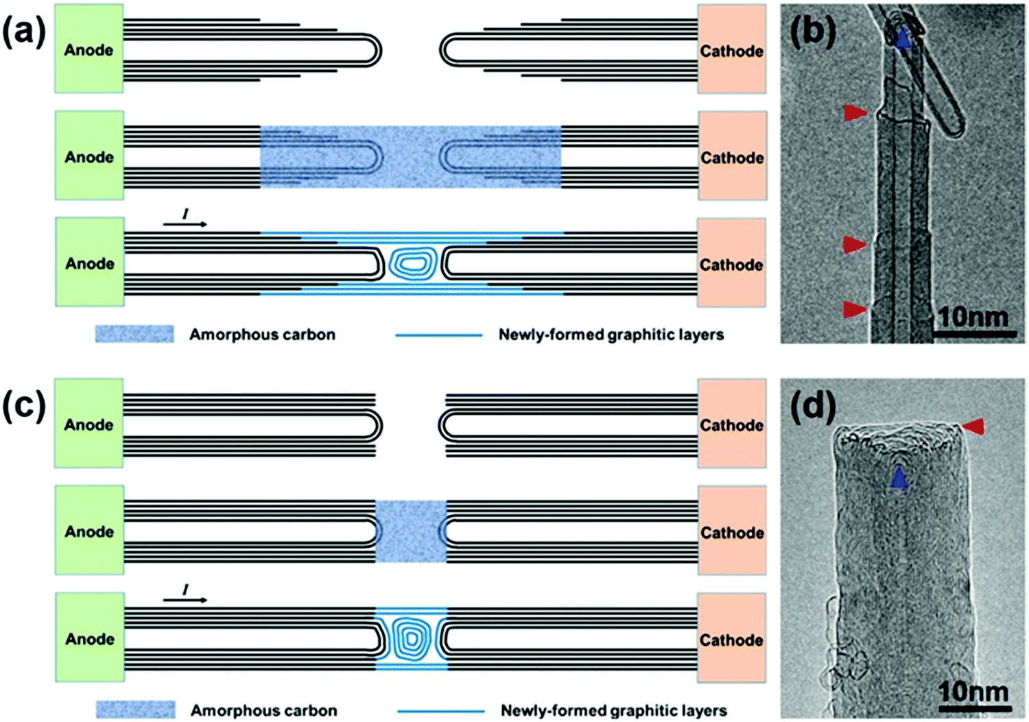 | ||
| Fig. 1 Schematic illustration of the seamless joining processes between the nanotube segments obtained in two different breakdown modes. (a) Seamless joining of two step-like CNT segments. (b) HRTEM image showing the step-like CNT morphology. (c) Seamless joining of two CNT segments with a regular open end. (d) HRTEM image showing the regular open-ended CNT morphology. The blue lines in (a and c) illustrate the newly-formed structures after the crystallization of a-C. The red arrowheads in (b and d) indicate the open edges of the broken shells, while the blue ones indicate the closed caps of inner tube shells. | ||
Fig. 2 shows a typical case of CNT repairing. A nanotube protruding from the edge of a gold wire was first selected by a piezo-driven tungsten tip. A current-induced annealing process was then carried out to minimize the contact resistance (Fig. 2a). The nanotube was intentionally cut by applying a voltage sweep up to 3 V, leaving behind the two step-like tube segments (Fig. 2b). Both tube segments had three closed-ended inner shells (1–3) and at least four open-ended shells (4–7) terminated at the tube surface, as indicated by the arrowheads in Fig. 2c (the two segments were brought into contact to reduce the thermal vibration for better HRTEM imaging). A certain amount of a-C was then deposited by electron beam induced deposition (EBID) to bridge the gap between the two opposite tube ends by focusing the e-beam at the joint region. Fig. 2d and e show the as-formed carbon hetero-structure with the central a-C as a joint. One may notice that the tube surface near the gap was also coated with a thin layer of a-C due to its deposition by dispersing the e-beam. Subsequently, a Joule heating induced crystallization process of the a-C was initiated by passing a high current through it (limited below 100 μA to avoid the breakdown of the junction). As evidenced in Fig. 2f, the a-C on the surface of the annealed junction had crystallized into continuous tubular shells that connected the two nanotubes seamlessly. The four continuous shells across the junction can be deemed as the result of epitaxial growth of graphitic layers along the tube surface that patched up the missing part of the broken shells (i.e. shells 4–7 as indicated in Fig. 2c). The open edges of the broken shells are expected to provide the nucleation sites for the graphene epitaxial growth, leading the newly-formed graphitic layers to incorporate into these existing shells. However, the interior a-C at the junction transformed into nano-onion structures, as pointed out by the red arrows in Fig. 2f. This phenomenon is quite similar to Huang's observations on the crystallization of a-C nanowires.24 Noticeably, the three inner tubes of the right-hand-side CNT segment (i.e. shells 1–3 in Fig. 2c) changed their cap structures and became distant from each other during the annealing process, as indicated by the blue arrows 1–3 in Fig. 2f. The existence of these closed structures (i.e. carbon onions and nanotube caps) led to a disconnected morphology inside the junction. Therefore, it is the outer continuous tubular shells that play an actual role in seamless CNT connection.
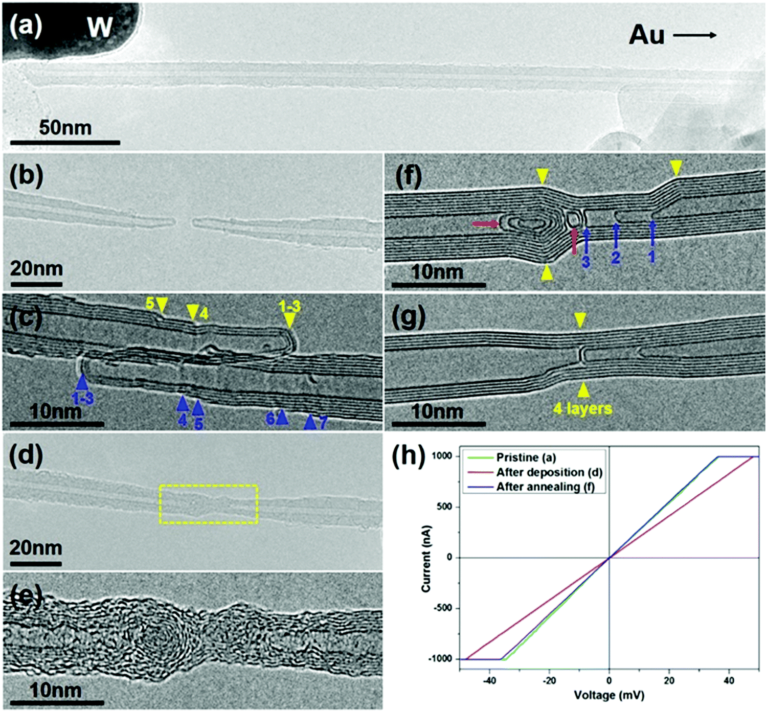 | ||
| Fig. 2 A series of TEM images showing the repairing process of a broken CNT. (a) Contact established between a W tip and a pristine nanotube protruding from a gold electrode. (b) Electrical breakdown of the nanotube after passing a large current through it. (c) HRTEM image showing the two ruptured CNT segments. (d) EBID of a-C at the gap between the two tube segments. (e) HRTEM image of the junction region as indicated in (d). (f) HRTEM image showing the junction after annealing. (g) HRTEM image of the junction after a prolonged annealing process. (h) The corresponding I–V curves recorded at different stages. | ||
The crystallization of a-C also leads to a significant improvement of the junction conduction. As revealed by the I–V curves recorded during the two-probe electrical measurements (Fig. 2h), the overall resistance was reduced from 48.1 kΩ to 36.1 kΩ after annealing, and the latter is almost the same as that of the pristine nanotube, i.e. 35.5 kΩ. This implies that many of the inner walls of this MWCNT did not participate in conduction, and the repairing of a few outer shells could be practically enough for the nearly full recovery of conduction. Interestingly, as the annealing process continued, the distinct kinks (as pointed out by the yellow arrowheads in Fig. 2f) almost disappeared and the tube walls became straighter and more regular (Fig. 2g). The inner closed structures changed a lot in morphology and some of them even vanished or slid away from the junction region, while the four outer shells largely maintained their structural integrity. This indicates that the kinks and closed structures are relatively unstable under a high current flux, and a prolonged annealing process can indeed improve the structural perfection of the joined tube shells (see ESI,† Fig. S1 for another example).
As for repairing two ruptured CNT segments with regular open ends, the crystallization of a-C at the gap caused a similar seamless joining process. The open edges of the outer broken shells can guide the formation of continuous tubular layers extending across the junction, whereas the a-C in the interior crystalized into closed nanostructures inside the channel, as shown in ESI,† Fig. S2 (or see the schematic illustration in Fig. 1c).
It should be pointed out that for CNT repairing, the two joined shells do not have to originate from the same tube wall of the pristine MWNT. In a typical case in the ESI,† Fig. S3, the outer and inner shells can be connected to form a continuous layer across the repaired CNT junction, although they had obviously different diameters and chiralities. Such a shell connection, therefore, provides the possibility of seamlessly connecting two MWNTs with completely different structural parameters.
We then tested the feasibility of this CNT joining process in more general situations, i.e. the two nanotubes to be joined are derived from different MWNTs. These CNT pairs may therefore have different chiralities, diameters, shell numbers or be connected in a non-straight shape. As depicted in Fig. 3a, a CNT segment obtained by electrical breakdown was controlled to approach another one to form a gap between them. These two MWNTs, both terminated with a regular open end, were apparently different in diameter and shell number (and supposedly in chirality as well) (Fig. 3b). The subsequent a-C deposition (Fig. 3c) and crystallization (Fig. 3d) also led to the CNT connection in a seamless pattern, regardless of their structural difference. As expected, the a-C crystallization caused a reduction of the overall resistance from 30.4 kΩ to 24.0 kΩ. The HRTEM image of the joined structure reveals that there were five continuous layers on the surface that made the CNT connection, as indicated by the yellow arrowheads in Fig. 3d. By comparing the morphologies of the right MWNT segment before and after connection, we conclude that the three outer shells along the CNT surface (shells 10–12) and two shells at the tube end (shells 8–9) participated in the five-shell connection (as indicated by the red arrowheads in Fig. 3b). The other inner shells (1–7), instead, were all capped by the crystallized carbon inside the junction. As a comparison, the outermost shell (shell 13, indicated by the blue arrowheads in Fig. 3b and d) remained unchanged upon annealing due to the lack of a-C in close proximity to its open edge. Similar results can be found on the left-hand-side MWNT segment: shells 12–16 involved in the five-shell connection, inner shells 1–11 capped during crystallization, while the outmost shell 17 almost unchanged. Unexpectedly, because of the uncontrolled drift of the W tip during the continued annealing, the bending junction finally evolved into a straight nanotube (three continuous layers were left across the straight junction due to the breakdown of the other two, as indicated by the yellow arrowheads in Fig. 3e). This demonstrates the surprising ability of sp2 carbon structures to adapt to the changed situations at elevated temperature, thus releasing the stress imposed by the external force.25
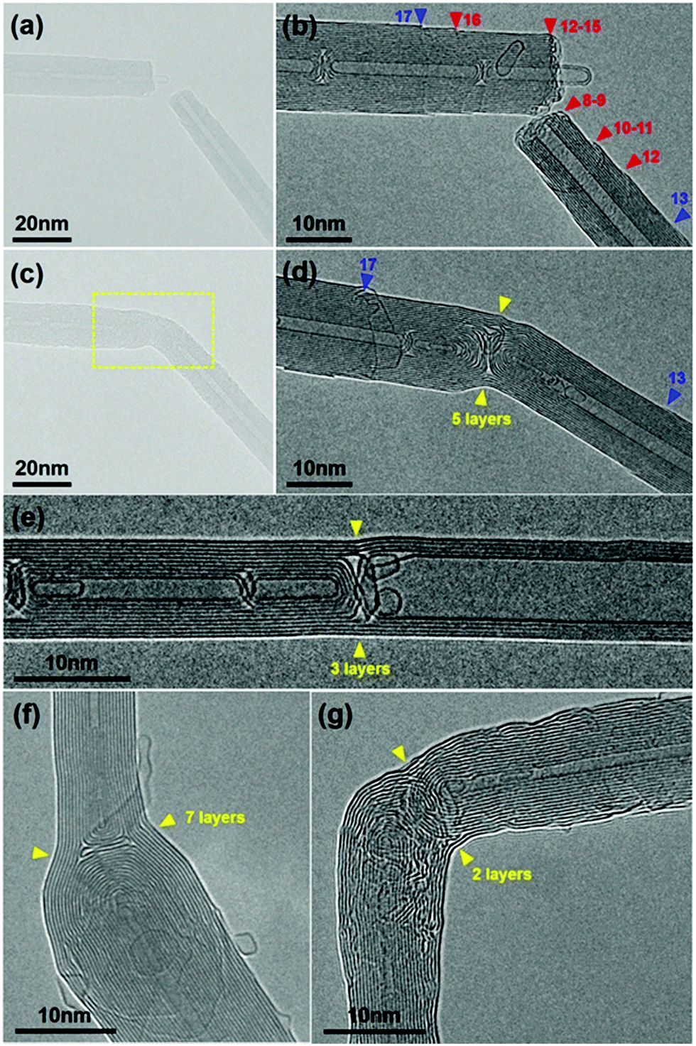 | ||
| Fig. 3 TEM images showing the seamless connection of two different CNTs. (a) Two nanotubes in close proximity to each other with a gap in between. (b) HRTEM image showing the end structures of these two nanotubes. The red arrowheads indicate the open shells to be connected. (c) EBID of a-C at the gap between the two nanotubes. (d) HRTEM image showing the junction (i.e. the boxed region in (c)) after annealing. (e) The bending junction evolves into a straight nanotube after a prolonged annealing process. The yellow arrowheads in (d and e) indicate the outer continuous shells crossing the junction. (f) Representative case of a seamless junction formed between thin and thick nanotubes. (g) Seamless right-angled CNT junction. | ||
Fig. 3f shows a more representative case for CNT connection between thin and thick nanotubes. In this case, there were seven layers across the junction that connect the 11-shell and 19-shell CNTs (see ESI,† Fig. S4 for more details). Moreover, this joining technique can be employed to create the seamless CNT junctions with any desired connecting angle, e.g. a right angle. Fig. 3g demonstrates such a junction, where the two outer graphitic layers, curved but continuous, seamlessly joined the two CNTs aligned perpendicular to each other (see Fig. S5, ESI,† for more details).
From the topological point of view, there must exist some non-six-membered ring defects, such as pentagons and heptagons, which can induce changes in chirality, diameter and even axis orientation across a junction. With the existence of such topological defects, the graphitic network formed by the crystallization of a-C shows great structural flexibility to join any two graphene cylinders. Thus, the tolerance for structural matching of two open-ended nanotubes based on our technique seems to be unlimited.
To develop a detailed understanding of the joining and crystallization process of the CNT junctions on an atomic scale, the reactive molecular dynamics (MD) calculations were performed under the NVT canonical ensemble by using the Reax/c code implemented in the LAMMPS package (see Methods for more calculation details).26,27Fig. 4a presents a straight CNT junction consisting of two (10, 10) SWNTs with an a-C node in between, which was created as the starting configuration for subsequent simulations. The a-C segment (red atoms in Fig. 4a) was generated by the liquid quench method.28,29 This model needs to be first thermalized at 300 K to obtain an equilibrated structure (the heated region is indicated in Fig. 4a), during which structural relaxation occurs and more C–C bonds are naturally established at the a-C/CNT interfaces (Fig. 4b1). Such an equilibrated model can be utilized to mimic the CNT junctions bridged by the deposited a-C in our experiments at room temperature. Considering that the noncatalytic crystallization of a-C needs a high temperature above 2500 °C,30 we then directly heated the equilibrated structure at 3500 K for 1 ns to simulate the crystallization/joining process of the heterojunction through Joule heating (Fig. 4b2). And it was finally cooled down to 300 K to obtain the annealed structure at room temperature (Fig. 4b3). Fig. 4c shows the total energy of the model as a function of simulation time during the above three stages. It can be observed that the junction reached a relatively stable state with small fluctuations in total energy for each stage, and the structure eventually evolved into a stable configuration with the lowest energy after annealing. The atomistic snapshots at the end of each stage (labeled with 1, 2 and 3 in Fig. 4c) are given in Fig. 4b. The detailed process of structural transformation can be clearly observed in Movie S1 in the ESI.† When heated to 3500 K, bond breaking and reconstruction occurred in the heated region of the model; carbon atoms partly transformed into a tubular structure with the graphitic basal plane roughly parallel to the SWNT axis, while other atoms underwent reconstruction into a fullerene-like structure encapsulated in the tubular layer (more clear in top view). This agrees well with our experimental results and the previous reports.24 After a cooling process, the annealed junction (model 3) maintained the configuration almost identical to that at the elevated temperature (model 2).
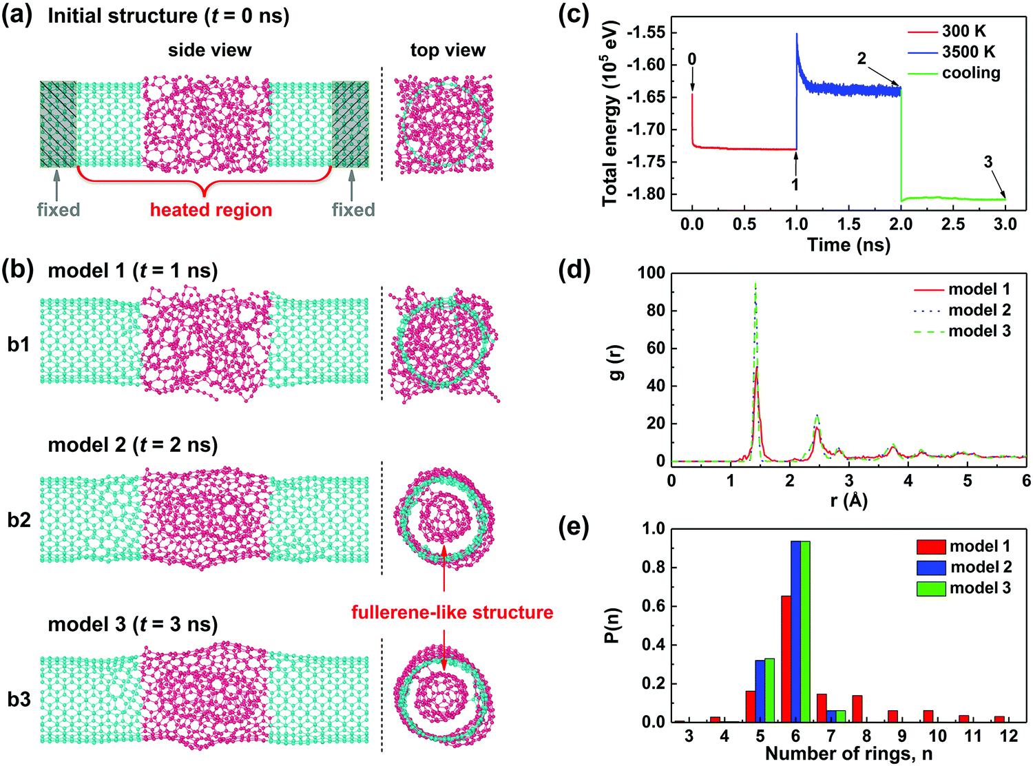 | ||
| Fig. 4 Crystallization of a straight junction consisting of two (10, 10) SWNTs joined by a central a-C node. (a) Starting configuration of the SWNT/a-C/SWNT junction. The gray-shaded regions are the fixed parts of the SWNTs to prevent them from rigid-body motions during the heating process, and the heated region is unfixed. (b) Atomistic snapshots of the junction at a simulation time of t = 1, 2 and 3 ns, corresponding to time points 1–3 in (c) respectively. (c) Total energy of the junction as a function of the simulation time. (d) Pair correlation functions and (e) ring size distribution of the junction models 1–3 (in the heated region). | ||
To further quantify the crystallization degree of the CNT junction (i.e. the heated region), the pair correlation functions and ring size distribution for junctions 1–3 were calculated, as depicted in Fig. 4d and e, respectively. We can see from Fig. 4d that all these three models have their first peaks centered at ∼1.42 Å, which corresponds to the sp2 hybridization bond-length, suggesting that the sp2-hybridized atoms dominate in all these structures. It is worth noting that the first peaks of junctions 2 and 3 are prominently higher and narrower than that of junction 1, revealing a higher degree of structural order in junctions 2 and 3. Actually, different from the all-sp2 bonding junctions 2 and 3, junction 1 contains many sp1 and sp3 hybridized bonds within the a-C joint and at the a-C/CNT interfaces. Similar results can also be obtained from the ring size distribution, as shown in Fig. 4e. Unlike the amorphous junction 1 that has many large-membered rings, junctions 2 and 3 have only six-membered rings and a small number of five- and seven-membered rings, building up the coherent tubular and fullerene-like structures. What is more, the above structural difference can be further verified by theoretical evaluation of their mechanical properties. The stress–strain curves during tensile loading and the corresponding structural evolution of junctions 1 and 3 are illustrated in the ESI,† Fig. S6. The results show that the tensile strengths of junctions 1 and 3 are 12 and 24 GPa, respectively, indicating a twofold increase in mechanical toughness caused by the crystallization of a-C.
In addition to CNT repairing as shown above, we also extended our considerations to more complicated situations where the two CNTs to be joined are different in axis orientation (Fig. 5a), chirality/diameter (Fig. 5b) or shell number (Fig. 5c), etc.Fig. 5 presents four different types of CNT/a-C/CNT junction models that were proposed to simulate their annealing/joining processes using the same calculation conditions as those in Fig. 4. After annealing, all these a-C joined junctions had transformed into graphitic structures and sp2 covalent binding was present throughout the entire junctions. Similar to the case in Fig. 4, the C atoms on the outer surface of the a-C joint crystalized into a tubular coherent network that merged into the outermost shells of the two counter CNTs, regardless of their difference in chirality, diameter and shell number. Thanks to the existence of 5/7 rings, an entirely coherent network can be always formed throughout the junction. Even in the case where two CNTs are aligned perpendicular to each other (as experimentally demonstrated in Fig. 3g), the outer shell was bent toward the different CNT axis directions to form the connections at the two intersections (Fig. 5a). This unambiguously demonstrates the unique ability of the C system to reconstruct itself into any sp2 graphitic configuration required for the existing CNT geometry at high temperature.
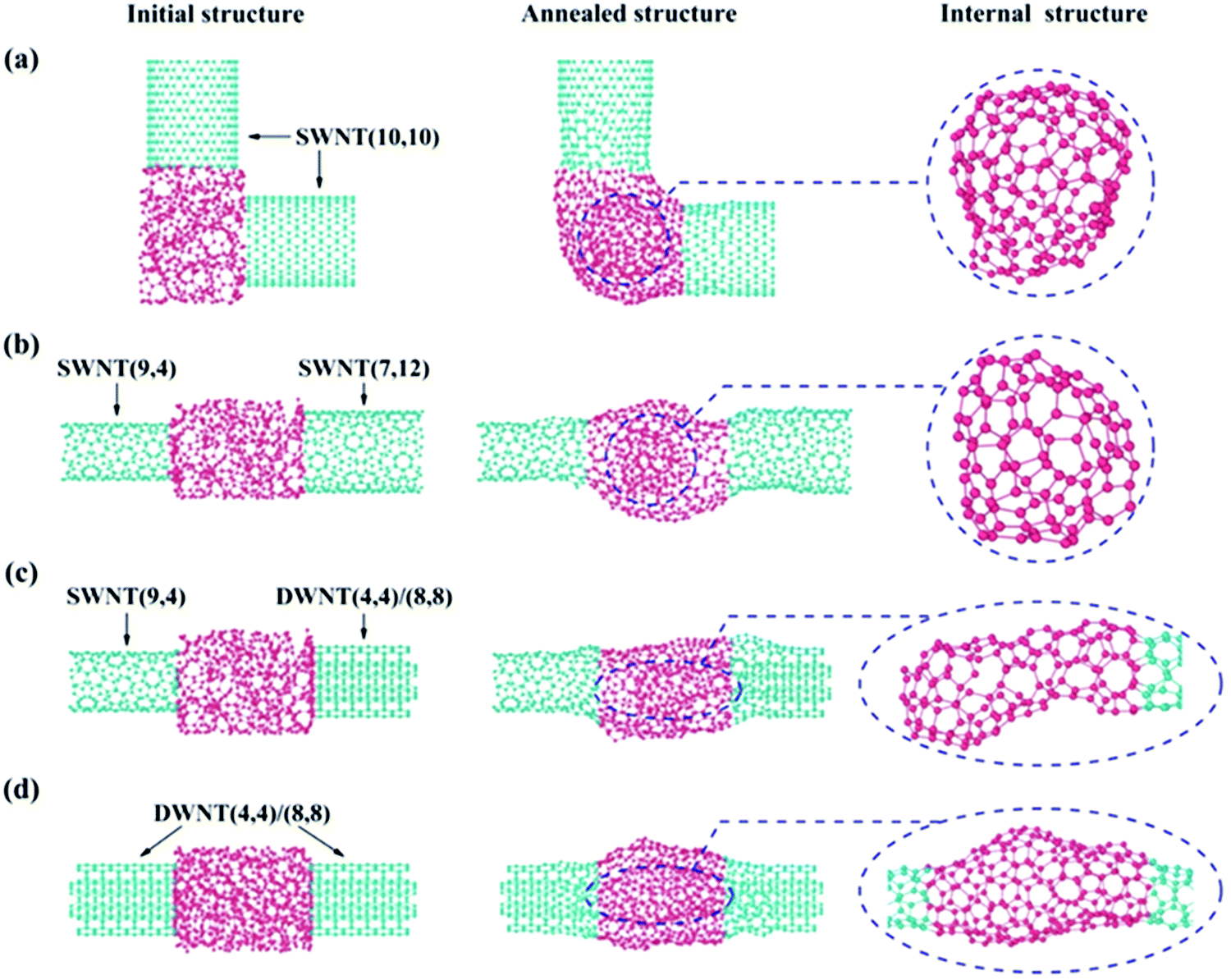 | ||
| Fig. 5 Seamless joining of two CNTs that are different in chirality, diameter, shell number and axis orientation. (a) Crystallization of the junction consisting of two SWNTs aligned perpendicular to each other. (b) Crystallization of the junction consisting of two SWNTs with different chiralities and diameters. (c) Crystallization of a SWNT/a-C/DWNT junction. (d) Crystallization of a DWNT/a-C/DWNT junction without forming closed structures inside the channel. | ||
The interior C atoms tend to transform into different closed sp2 carbon structures, depending on the junction type. For SWNT/a-C/SWNT junctions, a fullerene particle can always be observed, such as the cases in Fig. 4 and 5a, b. In the case of the SWNT/a-C/DWNT junction, due to the mismatch in the shell number for the two CNTs, the inner tube of the DWNT is capped by the interior C atoms to form a sealing structure (see the enlarged image circled with an ellipse in Fig. 5c). In the situation of MWNT/a-C/MWNT junctions, as documented in Fig. 3, both MWNTs may have their inner tubes capped inside the junction region. This structural complexity of the annealed junctions can be ascribed to not only the difference in CNT structures, but also the gap distance between CNTs and the amount of a-C, etc. Actually, if a junction is created with two CNTs of the same shell number, a small CNT gap and an appropriate amount of a-C, as the case in Fig. 5d, the two CNTs can be well connected without forming closed structures inside the junction. Both inner and outer shells of the two DWNTs are coherently joined through the two separate tubular graphitic layers. The atomistic arrangement of the inner connecting network can be clearly seen in the enlarged image of the circled region in Fig. 5d. The above results suggest that at elevated temperature, the a-C would spontaneously choose an evolution path to reach a configuration suited for the junction, during which the total energy could be effectively reduced by forming seamless connecting shells, nanotube caps or nano-onions.
Compared with the experimental results, the obtained atomistic networks by MD calculations exhibit rather irregular morphologies. On the one hand, this can be attributed to the short simulation time (1 ns) limited by our computation power. We believe that the structural quality can be improved by increasing the annealing time, just as the experimental case demonstrated in Fig. 2. On the other hand, the heating current flow used in our experiments, associated with a high electric field, can also strongly interact with the lattice due to the electro-migration effect.10 Therefore, the solid-state atom diffusion process may be more active, leading to the better graphitization of the annealed carbon structures.24
It needs to be noted that the SWNT segments used for simulation are all open ended, which is usually not the case for the real SWNTs, since small-diameter CNTs tend to close their ends to reach a low-energy structure, especially after electrical breakdown.11 Thus, the proposed method might not be applicable for the seamless connection of SWNTs. By contrast, the open-ended shells frequently appear in the pristine or ruptured MWNTs, and they therefore can be practically joined in a seamless fashion by using our method.
Finally, we successfully extended this technique to the seamless connection between different sp2 carbon allotropes, e.g. 1D nanotubes and 2D graphene (Fig. S7 in ESI†). A simplified structural model was proposed to illustrate the CNT–graphene connection via a coherent sp2 carbon network. In situ tensile tests revealed a bonding force of at least ∼670 nN for the junction (Fig. S8, ESI†). In addition, it is expected that more complicated sp2 carbon nanostructures, such as multibranched CNT junctions and integrated graphene sheets, etc., can be fabricated in a similar way.
Conclusions
In summary, we have presented a novel joining route for individual multiwalled CNTs by in situ TEM techniques. The process involves the amorphous–crystalline transition of the deposited a-C bridging the two nanotubes that is driven by running an electrical current through the junction. The crystallization of the a-C joint occurs in two distinct ways: the surface regions crystallized into continuous graphitic layers connecting the CNT shells, while the interior crystallized into closed structures. Such a seamless connection can be achieved between any two open-ended CNTs that are different in diameter, chirality, shell number and axis orientation, etc. MD simulations revealed the structural evolution during the CNT joining processes at the atomic scale, verifying the high flexibility of sp2 bonds to form complex coherent configurations. We further demonstrated the seamless joining process between individual CNTs and graphene sheets. The developed joining method is envisaged to be practically valuable in device applications, from CNT repairing and interconnecting in nanocircuits to the building of all-sp2 carbon systems.Methods
The in situ experiments were conducted using a FEI Talos-F200s TEM equipped with a TEM-STM holder. The multi-walled carbon nanotubes used in this work were synthesized by an arc-discharge method. The CNTs were assembled onto a freshly cut gold wire before each experiment by rubbing the gold wire on the CNT flake surface. (The graphene samples were prepared in the same way from a piece of highly oriented pyrolytic graphite.) This gold wire was then transferred and fixed by inserting the wire into a tiny-diameter pipe welded to the TEM-STM sample holder frame. An electrochemically etched tungsten wire (0.2 mm in diameter) was inserted into the three-dimensional movable part of the piezo-driven holder. The W wires have a nano-sized tip, convenient for in situ TEM electrical probing and manipulation. An electron beam induced deposition (EBID) process was used to construct the CNT junctions. The amorphous carbon can be accumulated at the gap between two CNTs simply by focusing the e-beam at the junction. Hydrocarbon molecules from air or the TEM column are adsorbed onto and migrate on the sample surface, which decompose into a-C when exposed to the e-beam. A crystallization process of the a-C was then initiated by passing through a high current that was carefully controlled to avoid the breakdown of the junction.All molecular dynamics (MD) simulations in this study were performed under the NVT canonical ensemble by using the Reax/c code implemented in the LAMMPS package. The ReaxFFC-2013 potential,31 a more accurate parameter set of ReaxFF for the solid carbon phase,32 was adopted to describe the interaction between the carbon atoms. A Nosé–Hoover thermostat and Newton's equations integrated using the velocity-Verlet algorithm were employed to control the temperature, and a time step of 0.25 fs was chosen to retain energy conservation. It should be noted that the heating rate was ignored because of the limitation of the MD time scale in all steps. Also due to the time scale limitation of MD simulations, the heating temperature (3500 K) employed in this simulation was relatively high compared to that in experiments, similar to simulations of many other carbon-based materials.33–35 The a-C used as the joint for a CNT junction (red atoms in Fig. 4a) was generated by the liquid quench method. The regions (shaded in grey in Fig. 4a) at the two ends of the SWNT junction were fixed to prevent the SWNTs from rigid-body motions during the heating process. The pair correlation functions and ring size distribution were calculated using the Isaacs software.36 For ring size counting, the criterion of Guttman was applied, and the cutoff radius was set at 1.73 Å.37
Conflicts of interest
There are no conflicts to declare.Acknowledgements
The authors would like to thank Jinming Wang of Xiamen University in China for a technical support in the course of this work. This work was financially supported by the National Natural Science Foundation of China (No. 61471307), the National Key R&D Program of China (Grant No. 2016YFA0202602), the Fundamental Research Funds for the Central Universities, the National Program for Thousand Young Talents of China, and the “Double-First Class” Foundation of Materials and Intelligent Manufacturing Discipline of Xiamen University.References
- L. Zhang, Y. Tang, Q. Peng, T. Yang, Q. Liu, Y. Wang, Y. Li, C. Du, Y. Sun, L. Cui, F. Yang, T. Shen, Z. Shan and J. Huang, Nat. Commun., 2018, 9, 96 CrossRef PubMed.
- Y. Lu, J. Huang, C. Wang, S. Sun and J. Lou, Nat. Nanotechnol., 2010, 5, 218–224 CrossRef CAS PubMed.
- M. S. Wang, D. Golberg and Y. Bando, Adv. Mater., 2010, 22, 93–98 CrossRef CAS PubMed.
- Y. Huang, X. Duan, Y. Cui, L. J. Lauhon, K. H. Kim and C. M. Lieber, Science, 2001, 294, 1313–1317 CrossRef CAS PubMed.
- P. J. Harris, Carbon, 2017, 122, 504–513 CrossRef CAS.
- F. Banhart, Nano Lett., 2001, 1, 329–332 CrossRef CAS.
- D. N. Madsen, K. Mølhave, R. Mateiu, A. M. Rasmussen, M. Brorson, C. J. H. Jacobsen and P. Bøggild, Nano Lett., 2003, 3, 47–49 CrossRef CAS.
- M. S. Wang, J. Y. Wang, Q. Chen and L. M. Peng, Adv. Funct. Mater., 2005, 15, 1825–1831 CrossRef CAS.
- M. Terrones, H. Terrones, F. Banhart, J. C. Charlier and P. M. Ajayan, Science, 2000, 288, 1226–1229 CrossRef CAS PubMed.
- M. Terrones, F. Banhart, N. Grobert, J. C. Charlier, H. Terrones and P. M. Ajayan, Phys. Rev. Lett., 2002, 89, 075505 CrossRef CAS PubMed.
- C. Jin, K. Suenaga and S. Iijima, Nat. Nanotechnol., 2008, 3, 17–21 CrossRef CAS PubMed.
- M. S. Wang, Y. Bando, J. A. Rodriguez-Manzo, F. Banhart and D. Golberg, ACS Nano, 2009, 3, 2632–2638 CrossRef CAS PubMed.
- J. A. Rodríguez-Manzo, F. Banhart, M. Terrones, H. Terrones, N. Grobert, P. M. Ajayan, B. G. Sumpter, V. Meunier, M. S. Wang, Y. Bando and D. Golberg, Proc. Natl. Acad. Sci. U. S. A., 2009, 106, 4591–4595 CrossRef PubMed.
- J. A. Rodríguez-Manzo, M. S. Wang, F. Banhart, Y. Bando and D. Golberg, Adv. Mater., 2009, 21, 4477–4482 CrossRef.
- A. Misra and C. Daraio, Adv. Mater., 2009, 21, 2305–2308 CrossRef CAS.
- S. Sharma, M. S. Rosmi, Y. Yaakob, M. Z. M. Yusop, G. Kalita, M. Kitazawa and M. Tanemura, Carbon, 2018, 132, 165–171 CrossRef CAS.
- C. Dekker, Phys. Today, 1999, 52, 22–28 CrossRef CAS.
- Z. Yao, C. L. Kane and C. Dekker, Phys. Rev. Lett., 1999, 84, 2941 CrossRef PubMed.
- X. Liang, S. Wang, X. Wei, L. Ding, Y. Zhu, Z. Zhang, Q. Chen, Y. Li, J. Zhang and L. M. Peng, Adv. Mater., 2009, 21, 1339–1343 CrossRef CAS.
- G. F. Close, S. Yasuda, B. Paul, S. Fujita and H. S. Wong, Nano Lett., 2008, 8, 706–709 CrossRef CAS PubMed.
- B. Li, X. Cao, H. G. Ong, J. W. Cheah, X. Zhou, Z. Yin, H. Li, J. Wang, F. Boey, W. Huang and H. Zhang, Adv. Mater., 2010, 22, 3058–3061 CrossRef CAS PubMed.
- X. Li, Y. Cheng, L. Zhao, Q. B. Zhang and M. S. Wang, Carbon, 2018, 133, 186–192 CrossRef CAS.
- P. G. Collins, M. S. Arnold and P. Avouris, Science, 2001, 292, 706–709 CrossRef CAS PubMed.
- J. Y. Huang, S. Chen, Z. F. Ren, G. Chen and M. S. Dresselhaus, Nano Lett., 2006, 6, 1699–1705 CrossRef CAS PubMed.
- A. V. Krasheninnikov and F. Banhart, Nat. Mater., 2007, 6, 723 CrossRef CAS PubMed.
- H. M. Aktulga, J. C. Fogarty, S. A. Pandit and A. Y. Grama, Parallel Comput., 2012, 38, 245–259 CrossRef.
- S. Plimpton, J. Comput. Phys., 1995, 117, 1–19 CrossRef CAS.
- G. Galli, R. M. Martin, R. Car and M. Parrinello, Phys. Rev. Lett., 1989, 62, 555 CrossRef CAS PubMed.
- R. Ranganathan, S. Rokkam, T. Desai and P. Keblinski, Carbon, 2017, 113, 87–99 CrossRef CAS.
- B. T. Kelly, Physics of Graphite, Applied Science Publisher, London, 1981 Search PubMed.
- S. G. Srinivasan, A. C. T. Van Duin and P. Ganesh, J. Phys. Chem. A, 2015, 119, 571–580 CrossRef CAS PubMed.
- A. C. T. Van Duin, S. Dasgupta, F. Lorant and W. A. Goddard, J. Phys. Chem. A, 2001, 105, 9396–9409 CrossRef CAS.
- I. Jang, S. B. Sinnott, D. Danailov and P. Keblinski, Nano Lett., 2004, 4, 109–114 CrossRef CAS.
- L. He, J. Q. Lu and H. Q. Jiang, Small, 2009, 5, 2802–2806 CrossRef CAS PubMed.
- Y. Yao, K. K. Fu, S. Zhu, J. Dai, Y. Wang, G. Pastel, Y. Chen, T. Li, C. Wang, T. Li and L. Hu, Nano Lett., 2016, 16, 7282–7289 CrossRef CAS PubMed.
- S. L. Roux and V. Petkov, J. Appl. Crystallogr., 2010, 43, 181–185 CrossRef.
- L. Guttman, J. Non-Cryst. Solids, 1990, 116, 145–147 CrossRef CAS.
Footnotes |
| † Electronic supplementary information (ESI) available. See DOI: 10.1039/c8mh01154k |
| ‡ These authors contributed equally to this work. |
| This journal is © The Royal Society of Chemistry 2019 |