
 Open Access Article
 This Open Access Article is licensed under a
 Creative Commons Attribution 3.0 Unported Licence
Spatially resolved solid-state reduction of graphene oxide thin films†
Maria C.
Morant-Miñana
 *ab,
Jonas
Heidler
b,
Gunnar
Glasser
b,
Hao
Lu
b,
Rüdiger
Berger
b,
Nerea
Gil-Gonzalez
c,
Klaus
Müllen
b,
Dago M.
de Leeuw
d and
Kamal
Asadi
*b
*ab,
Jonas
Heidler
b,
Gunnar
Glasser
b,
Hao
Lu
b,
Rüdiger
Berger
b,
Nerea
Gil-Gonzalez
c,
Klaus
Müllen
b,
Dago M.
de Leeuw
d and
Kamal
Asadi
*b
aCIC energiGUNE, Parque Tecnologico de Alava Albert Einstein 48, ED. CIC 01510 Miñano, Spain. E-mail: mmorant@cicenergigune.com
bMax-Planck-Institut for Polymer Research, Ackermannweg 10, 55128 Mainz, Germany. E-mail: asadi@mpip-mainz.mpg.de
cCEIT-IK4 Paseo Manuel Lardizábal 15, 20018 San Sebastián, Spain
dDelft University of Technology, Kluyverweg, 2629 HS, Delft, The Netherlands
First published on 7th September 2018
Abstract
Re-establishment of electrical conductivity in graphene oxide (GO), the insulating form of graphene, is (partially) accomplished by reduction through high temperature treatments in a reducing atmosphere, or using strongly reducing chemicals or electrolytic processes. The reduction methods are suited for bulk graphene oxide. Spatially resolved reduction of thin films of graphene oxide is important for a wide range of applications such as in microelectronics, where an electrolyte-free, room temperature reduction process is needed. Here, we present spatially resolved solid-state reduction of graphene oxide thin films. We demonstrate that the reduction mechanism is based on electrolysis of water that is adsorbed on the graphene oxide thin film. The reduced graphene oxide thin-films show sheet resistance of only several kOhm, with weak temperature dependence. Graphene oxide can be produced on a large scale and processed using low-cost solution casting techniques. Spatially resolved re-establishment of conductivity in GO can be used in electrically controlled water permeation or in micro- and nanoelectronic applications for instance as an anti-fuse.
Conceptual insightsThe current paradigms at both the industrial and research levels produce reduced graphene oxide (rGO), an imperfect form of graphene, only in the bulk form. For a wide range of applications, from microelectronics to water permeation, spatially resolved and controlled reduction of GO in (thin-) films is needed. Such applications require a paradigm shift in the reduction process, which should be free from intentionally used auxiliaries such as electrolytes and high temperatures. This manuscript demonstrates how to control reduction of GO thin-films at room temperature with spatial resolution simply by application of a voltage, without the intentional use of electrolytes. This work demonstrates the underlying fundamental reduction mechanism and its kinetics. Achieving and controlling spatial resolution in reduction have a broad impact on the application of GO. The insight gained here can shed light on many of the fundamental processes that take place during electrically controlled water permeation through GO (very recently demonstrated). Furthermore, spatial resolution of the reduction process is crucial for the applications of rGO in microelectronics in for instance anti-fuses. |
Introduction
Graphene oxide (GO), a partially oxidized form of graphene, is a wide bandgap insulator that unlike graphene can be produced on a large scale at low costs. Due to the presence of oxygen-containing functional groups on the surface, GO can be easily dispersed in water, yielding a stable colloidal suspension thereby enabling solution processing.1 Electrical conductivity can be restored, at least partially, by reducing GO and re-establishing C![[double bond, length as m-dash]](https://www.rsc.org/images/entities/char_e001.gif) C sp2 bonds. Despite the fact that complete reduction of GO is still a challenge,2 reduced graphene oxide (rGO) has been successfully used for low-cost applications and solution processable electronic devices3 such as field-effect transistors,4 solar cells,5 transparent conductive films,6 supercapacitors, and electrically controlled water permeation.7–10
C sp2 bonds. Despite the fact that complete reduction of GO is still a challenge,2 reduced graphene oxide (rGO) has been successfully used for low-cost applications and solution processable electronic devices3 such as field-effect transistors,4 solar cells,5 transparent conductive films,6 supercapacitors, and electrically controlled water permeation.7–10
Thermal, chemical and electrochemical methods are the most common strategies in producing rGO. Thermal annealing in a controlled reducing atmosphere of Ar/H2 produces rGO with high degree of reduction and relatively high conductivity in bulk form.11,12 To furnish rGO via chemical routes, strong reducing and typically toxic chemicals such as hydrazine hydrate, are used.13–15 Electrochemical reduction of GO is usually performed from aqueous colloidal suspensions in the presence of a buffer electrolyte.16,17–20 The electrolyte plays a critical role in the quality of the final rGO and, concomitantly, its electrical conductivity.21,22
Recently it has been reported that GO thin films deposited on an Au coated substrate show enhanced conductivity upon application of a potential difference between either the metallic tip of an atomic-force microscope (AFM) in contact mode or a scanning tunneling microscope tip (STM) and the bottom Au contact.23–26 No liquid electrolyte has intentionally been used. Different mechanisms have been proposed for the enhanced conductivity. It has been argued that the conductivity enhancement is due to the reduction of GO in an electrochemical process initiated by the voltage applied to the tip,27 and that the process is reversible. On the other hand, density functional theory (DFT) calculations have suggested that the strength of the applied external electric field is the driving force for the enhanced conductivity.28 Finally, it has been suggested that the increase in conductivity is current driven,29–31 and the reduction process is sensitive to the humidity of the environment.32,33 There are still many open questions regarding the reversibility of the reduction process34 and a general consensus is still missing.
Spatially resolved solid-state reduction of graphene oxide on the micro- and nanoscale simply by application of an electric potential is of technological interest. A breakthrough in spatial reduction allows realization of rGO-based interconnects or anti-fuses.35 The anti-fuse or interconnect formation is typically the last step in a microelectronics manufacturing process, wherein a thin film of a highly resistive material sandwiched between two contacts, is made conductive by application of a bias over the contacts at temperatures below 150 °C.36 Anti-fuses based on GO should then be realized by local reduction of thin solid films of GO, simply by application of a bias over the film. GO-based anti-fuses have not yet been demonstrated.
Here, we present the spatially resolved solid-state reduction of graphene oxide thin films in a humidity controlled atmosphere as a first step towards the development of a GO-based antifuse. We unambiguously show that the reduction is an irreversible electrochemical process driven by the electrolysis of water that is supplied from the gas phase. Due to water electrolysis, conductive rGO dendrites irreversibly grow from the working to the counter electrode. The reduction of GO was confirmed by scanning Raman and X-ray photon spectroscopy (XPS). We present a mechanistic model to explain the bias and time dependence of the reduction process. The sheet resistance of 10 kOhm per square obtained after reduction of the GO thin-film shows a weak temperature dependence, Eact of only 12 meV, down to 30 K indicating the formation of a highly electrically conductive rGO film. Using lithographically patterned structures spatially resolved rGO thin-films could be realized.
Experimental section
Fabrication of test structures
Silicon monitor wafers with a thermally grown SiO2 layer of 200 nm were used as substrates. The wafers were cleaned using acetone and subsequently an ethanol ultrasonic bath for 5 minutes prior to use. Test structures were realized using conventional I-line photolithography.37 Test structures comprising both interdigitated and circular concentric electrode configurations were fabricated. Au (50 nm) was used as the contact with Ti (2 nm) as an adhesion layer. The spacing, L, and width, W, between the Au electrodes was varied between 0.75 μm and 50 μm, and between 1000 μm and 11![[thin space (1/6-em)]](https://www.rsc.org/images/entities/char_2009.gif) 000 μm, respectively. The schematic of the test structures are shown in Fig. S1 in the ESI.†
000 μm, respectively. The schematic of the test structures are shown in Fig. S1 in the ESI.†
Prior to graphene oxide deposition, the substrates were cleaned using acetone and subsequently ethanol ultrasonic baths for 5 minutes. To promote wettability of the substrates, the surface was treated with a UV/O3 plasma for 30 min. Water dispersions of graphene oxide (4 mg ml−1) were purchased from Graphenea, Spain, and used as received. To obtain a homogeneous dispersion, the solution was sonicated for 1 hour in a 40 Hz ultrasonic bath. Thin-films were formed by depositing a drop from a homogeneous water dispersion of GO (4 mg ml−1) on the test patterns (Fig. 1a). The GO films were further dried in a vacuum at 80 °C. The thickness of the GO film amounted to 300 nm. Thinner films were obtained by diluting the GO dispersion. By adding deionized water, the stock solution of GO was diluted to 1.5, 0.75, 0.37 and 0.18 mg ml−1, from which thin-films of different thicknesses of 115, 60, 30, and 10 nm were obtained, respectively. GO suspensions were drop-cast on the test substrates and dried at room temperature overnight.
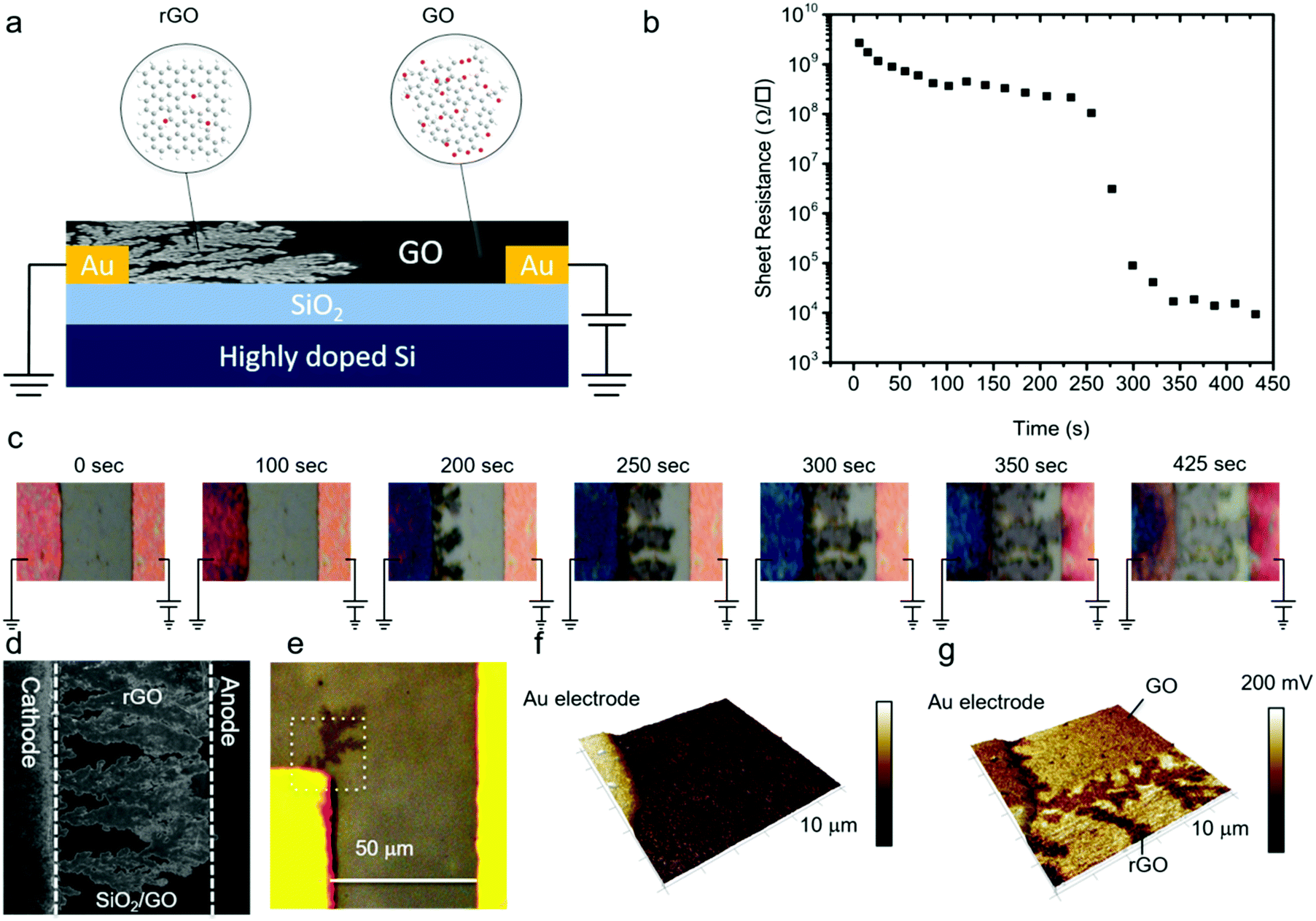 | ||
| Fig. 1 Growth of dendrites in GO. (a) Scheme of the measurement setup, where a GO thin-film is deposited onto a Si/SiO2 substrate comprising lithographically patterned Ti/Au electrodes. A constant DC bias of +3 V is applied on the anode. Dendrites grow from the cathode to the anode. (b) Evolution of sheet resistance of a GO thin film with time upon continuously applying +3 V bias on the anode. The sheet resistance was obtained using a four-point-probe configuration. (c) Corresponding real-time optical images of the GO thin-film with applied bias as a function of time. The distance between the electrodes is 50 μm. The schematically drawn bias and ground connections solely indicate the anode and cathode, respectively. All the DC electrical measurements were performed using a four-point-probe configuration. (d) SEM image of the dendritic rGO that bridged the anode and cathode. (e) The optical image of the spot used for AFM imaging wherein a dendrite is clearly visible in the optical contrast. (f) AFM topography image of the dotted area in (e), and (g) is the corresponding contact potential difference (CPD) imaged with KPFM. Here the 3D topography was overlaid with the local CPD map. The color scale bar corresponds to a CPD difference of 200 mV. | ||
Device characterization
Electrical characterization was performed under both dynamic vacuum and ambient conditions (room temperature and relative humidity of 25 °C and 45% respectively), as well as under controlled humidity conditions. For every measurement a fresh test structure without prior history was used. For DC measurements a Keithley 4200-SCS Semiconductor Characterization System was employed. Electrochemical measurements were performed with a μAutolabIII/FRA2 from Metrohm Autolab. Cyclic voltammetry measurements at different humidity levels were performed on a home-made sealed probe station. The humidity level was controlled using N2 and a gas bubbler. To obtain a relative humidity higher than 45%, synthetic air was passed through a gas bubbler filled with water. Low humidity levels were achieved by flushing dry N2 into the chamber.Analytical characterization
Optical images were taken in reflection mode using a Polyvar optical microscope. AFM measurements were performed using a Nanoscope Dimension Icon in peak force mode. The KPFM measurements were performed in frequency mode with PPP-EFM cantilevers (Nanosensors GmbH). Scanning electron microscope images were taken using a Zeiss 1530 Gemini SEM. Scanning Raman spectroscopy was recorded with a Bruker RFS 100/S spectrometer operating at a laser wavelength of 532 nm. The Raman spectra were normalized to the intensity of the 2D peak (2700 cm−1) after the baseline correction.X-ray photoelectron spectroscopy (XPS) was conducted with a Kratos Axis UltraDLD spectrometer (Kratos, Manchester, England) using Kα excitation of an Al source with a photon energy of 1487 eV. The data were acquired in the hybrid mode with a measurement size of 300 × 700 μm2 using a 0° take-off angle, defined as the angle between the surface normal and the axis of the analyzer lens. A charge neutralizer was always used during spectra collection to compensate for charge build-up on the samples. Survey and detailed region XP spectra were collected by setting the analyzer pass energy at 80 eV; C 1s and O 1s high-resolution spectra were collected with an analyzer pass energy of 20 eV. A neutralizer was always used during spectra collection. To avoid beam damage, the spectra collection time was constrained within 2 minutes and several separate spots were measured for each sample. Atomic compositions were calculated by subtracting a linear background from the collected spectra by setting the analyzer pass energy at 80 eV. The peak areas were normalized by the manufacturer supplied sensitivity factors, and atomic compositions were calculated accordingly with CasaXPS software.
Results and discussion
Dendrite formation
GO thin-films were formed by drop-casting on the test structures with Au electrodes. We note that for every single measurement a fresh device without any prior bias history was used. The samples were equilibrated for at least ten minutes before any measurement was started. A positive bias was applied to the working electrode and the counter electrode was grounded. The sheet resistance of the GO film was monitored with time and, simultaneously, optical images were recorded. Electrical measurements were performed under ambient conditions at 23 °C and 45% relative humidity. In a first step, a low fixed bias voltage of +1 V was applied. A high sheet resistance of about 1.2 × 10⁹ Ω □−1 was measured, which remained constant over time. Under these conditions, no changes were observed in the optical images over a period longer than 5 hours.In the next step, the electrical measurement was performed using a bias of +3 V. The sheet resistance as a function of time, Fig. 1b, slightly decreased from the initial value of 1.2 × 10⁹ Ω □−1 to 3.3 × 10⁸ Ω □−1 and then suddenly dropped by orders of magnitude to 9.5 × 10³ Ω □−1. The corresponding optical images are presented in Fig. 1c. In the early stages, there was no change in the contrast of the GO film. However, as time elapsed, the contrast of the GO film deposited on the grounded counter electrode changed; dark dendritic structures appeared at the edge of the grounded electrode that grew in time. Scanning electron microscopy (SEM) images, Fig. 1d, revealed formation of the dendritic microstructure in the GO thin-film. In order to probe signatures of the dendritic structures, we performed atomic force microscopy (AFM). The AFM tip was positioned in an area close to the Au cathode where dendritic structures were visible by optical microscopy (Fig. 1e). The area marked in the white square was imaged. The AFM topography image, Fig. 1f, shows that there is no change in the height of the GO thin film due to the formation of the dendritic structures. However, there was a contrast in the contact potential difference (CPD) imaged with Kelvin probe force microscopy (KPFM), Fig. 1g. The CPD values for the GO were 50–100 mV higher as compared to rGO. The dendritic structure could be detected within the GO matrix. This finding suggests the conductive nature of the dendrites with respect to the surrounding GO matrix. Hence, the growth of dendrites from the grounded counter electrode, the cathode, to the positively biased working electrode, the anode, renders the insulating GO conducting.
A dramatic drop in sheet resistance was always observed as soon as the first dendrites bridged the gap between the electrodes. With further increase of the measurement time, the dendrites continued to grow until the whole area between the electrodes was fully covered. The reduction time, i.e. the time at which the sheet resistance dramatically dropped, did not depend on the width of the electrodes, which implies that the growth of dendrites is a one-dimensional process. Furthermore, a conducting channel could be always formed at voltages between +2 V and +2.5 V regardless of the electrode spacing. Hence, the dendrite formation process is not driven by the electric field, but completely dominated by the applied bias, suggesting electrochemical reactions.
In the next step, the test structures were placed in a high vacuum of 10−6 mbar. Electrical measurements were performed by continuously applying a +3 V bias. The sheet resistance did not change with time. Biases as high as +10 V were applied, but the sheet resistance remained constant at the initial high value of 1.2 × 10⁹ Ω □−1. Also the optical images did not change; the high vacuum impeded the growth of dendrites.
Characterization of rGO dendrites
To determine the chemical nature of the dendritic products in the GO film, scanning Raman spectroscopy and X-ray photoelectron spectroscopy (XPS) measurements were performed. First, GO was partially reduced by applying +3 V on the Au electrode. Raman measurements were performed on the boundary between dendrites and the unaffected GO film. To decrease as much as possible the structural effects on GO induced by the Raman laser,38–40 the integration time, the scan average, the laser wavelength and the laser doses were optimized. The optical image of the investigated spot is presented in Fig. 2a. The areas corresponding to GO and rGO are marked. Representative local Raman spectra of regions are presented in Fig. 2d. The normalized spectrum measured in the dark brown area exhibits the three main characteristic peaks of GO: the D mode at 1357.0 cm−1, the G mode at 1590.5 cm−1 and the 2D mode at 2738.6 cm−1. The D and G modes have almost the same intensity (ID/IG = 0.84), which is indicative of high structural disorder caused by the random distribution of oxidized areas with oxygen-containing functional groups. The normalized Raman spectrum of the light brown region shows a relative increase in the intensity of the D peak (ID/IG = 1.54), which is characteristic of the high-density defect regime and reflects a relative increase of sp2 domains.41,42 The Raman spectra therefore provide evidence that the dendrites consist of rGO.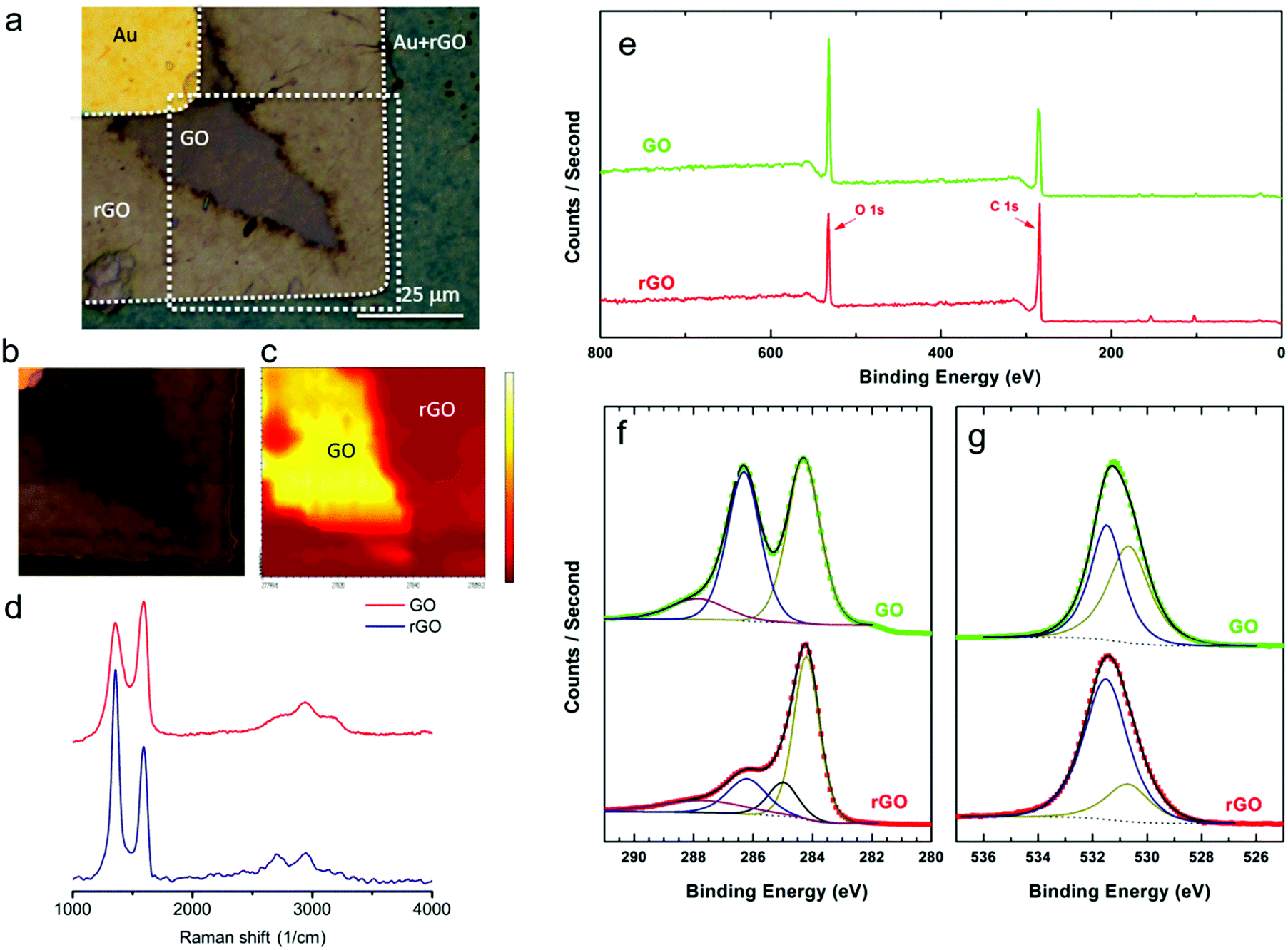 | ||
| Fig. 2 Chemical nature of the dendrites. (a) Optical image of a partially reduced GO film. The Au anode is on the top left corner with unchanged color contrast. The Au cathode changes in contrast due to reduction of GO. The dark brown color in the channel is remaining GO whereas the light brown color is rGO. (b) The marked region shows the area that is used for 2D scanning Raman spectroscopy. (c) 2D-Raman spectra (G-mode) mapping at the edge of a reducing front highlighted by a dashed square in (a). The scale bar is from 0 to 1.2 × 10⁶ counts. (d) Representative normalized Raman spectra measured at different spots of the sample for GO (D mode at 1357.0 cm−1, G mode at 1590.5 cm−1 and 2D mode at 2738.6 cm−1) and rGO (D mode at 1363.5 cm−1, G mode at 1583.7 cm−1 and 2D mode at 2703.1 cm−1). (e) XPS survey of GO and electrically conductive rGO using a photon energy of 1487 eV. High-resolution spectra for C 1s (f) and O 1s (g) peaks measured for GO and rGO, and the corresponding deconvolutions. | ||
A two-dimensional map of the Raman spectra of the marked region in Fig. 2a was obtained and is presented in Fig. 2c. The map was extracted from the intensity of the G mode (1590 cm−1), by taking point-by-point Raman spectra of the indicated area. The color map is based on an intensity color scale with yellow and red corresponding to the high and low intensity regions, respectively. The 2D Raman map clearly shows that the area under investigation is composed of two distinct regions of rGO and GO.
In order to quantify the extent of reduction we first reduced the GO layer at +3 V. Remaining GO was washed away with water. Subsequently, XPS spectra were measured to quantify the degree of reduction. XPS spectra were taken from rGO between the Au electrodes and from GO on the bare substrate far away from the electrodes. The survey spectra of as deposited GO and rGO are presented in Fig. 2e. With increasing binding energy, the marked emissions can be assigned to Si 2p (101 eV), Si 2s (152 eV), C 1s (284 eV) and O 1s (532 eV). Clearly, the relative intensity of O 1s photoemission with respect to C 1s is reduced for rGO as compared to GO. A close up of the C 1s and O 1s X-ray photoemission spectra are presented in Fig. 2f and g, respectively. The XPS spectra were self-fitted according to the Voigt function, after performing a Shirley background subtraction.43 The C 1s spectrum of GO was deconvoluted into three peaks corresponding to different types of carbon species. The peaks were centered at 284.2, 286.2 and 287.8 eV corresponding to C sp2, combination of C–O and CO, and COO, respectively.6,13,44 By contrast, the deconvoluted spectrum of rGO is dominated by the emission peak from C sp2. The amount of C–O, CO and COO bonds has substantially been reduced. Moreover, a fourth peak, centred at 285 eV and corresponding to C–C sp3 bonds, needs to be introduced in order to reproduce the experimental rGO spectrum.
The O 1s spectrum of GO can be mainly deconvoluted into two peaks. The peaks centred at 530.7 eV and 531.5 eV are assigned to COO bonds and to O atoms directly bonded to carbon C–O, respectively.45–47 The O species existing in OH or bonded to aromatic C, appearing at binding energies above 533 eV,48 cannot be excluded; the spectra components for these species were weak and superimposed by the peak at 531.5 eV. The O from absorbed water (>534 eV) is not detected since the water species are evaporated in the ultra high vacuum.49 In accordance with the C 1s spectra, the O 1s spectrum of rGO is dominated by the reduced C–O states, despite the fact that no complete reduction of the oxygen-containing functional groups has been achieved.
The degree of reduction in rGO was obtained by calculating the spectral weight of the C sp2 contribution within the whole C 1s region. The sp2 percentage was found to be 47% and 55% for GO and rGO, respectively. It has been shown that a small increase in sp2 fraction yields substantially enhanced electrical conductivity.50 Finally, using the XPS data, the elemental composition percentage was determined to be 71.4 ± 1.2 (C) and 28.6 ± 1 (O) for GO and 79.8 ± 1 (C) and 20.8 ± 0.8 (O) for rGO.
Reduction mechanism
To pinpoint the reduction mechanism, we performed two-electrode cyclic voltammetry (CV) measurements both on a pristine GO thin-film and on a demi-water droplet deposited on the substrate. The electrode spacing was 50 μm. One electrode was taken as the working electrode and the other one as the counter electrode. The CV diagrams were obtained at a low sweep rate of 0.1 V s−1. We first measured CV for a GO layer deposited on the test structure. The CV curve of GO, Fig. 3a, showed that the current passing through the GO film slowly increased from 0 to 10 μA as the voltage increased from 0 to about 3.2 V. Subsequently, the current increased exponentially with the applied bias, indicative of the complete reduction of the GO film. Upon scanning back, the current remained high at about 5 mA, which indicated that the formation of rGO is an irreversible process. The formation of rGO is confirmed by the quasi-rectangular shape of the CV curve indicating a capacitive behavior typical of an electrical double-layer. Electrical energy can be stored at the electrode–electrolyte interface when a voltage bias is applied.51 Thus, increased scan rate results in an increase of the discharge current of the CV demonstrating an ultrafast charging and discharging capability.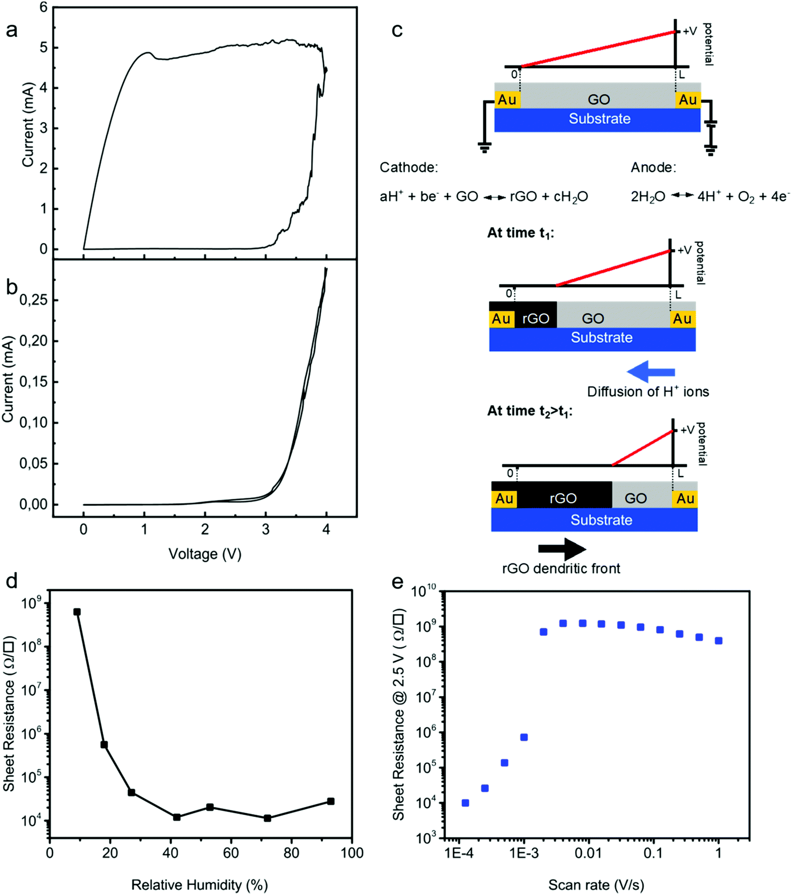 | ||
| Fig. 3 Spatially resolved solid-state GO reduction mechanism. (a) CV measurement on a GO film. The scan rate was 0.1 V s−1. The inset shows the second CV measurement after reduction of GO to rGO on a linear scale. (b) The CV curve of only demi water. The measurements in (a) and (b) were performed at an ambient temperature of 23 °C and humidity of 45%. (c) Schematic of the reduction process, where water is oxidized at the anode, the working electrode. The H+ ions diffuse towards the grounded cathode, the counter electrode, and reduce GO leading to rGO dendrite growth from the cathode to the anode. Since GO exhibits a very high sheet resistance, the potential drops linearly from the anode to cathode. The potential drop over the conducting rGO is disregarded. (d) Influence of humidity on the sheet resistance obtained after a single bias swept from 0 V to +4.5 V at a scan rate of 0.01 V s−1 at an ambient temperature of 23 °C. (e) Sheet resistance as a function of bias scan rate obtained after a single bias swept from 0 V to +4.5 V at an ambient temperature of 23 °C and relative humidity of 45%. The electrode spacing was 50 μm for all CV measurements. | ||
The CV curve of demi water deposited on the test structures was subsequently measured under identical conditions, and is presented in Fig. 3b. The oxidation peak is observed at around ∼3.2 V. In a conventional electrochemical cell, water electrolysis takes place at an electrode potential of 1.26 V; hence, the overpotential is about 2 V. This overpotential is due to the special geometry of the electrochemical cell, using two Au electrodes and is in good agreement with predictions from DFT calculations for electrolysis on ideal polarizable electrodes such as Au.52,53
More importantly, the CV curves of the GO film and demi water at high bias coincide. This means that the oxidation of water is the rate determining step for the reduction of GO. The two-step mechanism is as follows. First water is oxidized at the anode:
| 2H2O ⇆ 4H+ + O2 + 4e− | (1) |
| aH+ + be− + GO ⇆ rGO + cH2O | (2) |
The reduction mechanism is schematically depicted in Fig. 3c. Water is oxidized at the anode and H+ ions are formed, which diffuse towards the cathode and reduce GO. Due to the high resistance of the GO film, the reduction is not homogeneous in the channel. Starting from a pristine GO film, due to the high resistance the potential varies linearly from the cathode to anode. Only close to the cathode is the potential low enough to reduce GO. The rGO formed is a good electrical conductor and, therefore, the potential drop over the formed rGO can be disregarded. The remaining GO film remains highly resistive; there is no current flowing through the GO film and the potential therefore varies linearly from the boundary between GO and rGO to the anode. Subsequent reduction then takes place at this boundary. This means that the effective channel length decreases, and that the dendrites of rGO grow in a front from the cathode to anode. During this growth the sheet resistance remains high, until the first conducting rGO dendrites cross the electrode spacing. This two-step electrochemical mechanism readily explains that the GO reduction is a one-dimensional process. Therefore, the reduction time is independent of the width of the electrode. To further substantiate the mechanism, we investigated the reduction kinetics, meaning we varied the relative humidity, the scan rate as well as the applied potential, and measured the sheet resistance and reduction time. To demonstrate that water is a crucial component, we performed single CV sweeps as a function of relative humidity. The bias was swept from 0 V to 4.5 V. We used a scan rate of only 0.01 V s−1 to mimic quasi-static measurements. The sheet resistance after the sweep is presented in Fig. 3d as a function of relative humidity. At zero humidity, i.e. in a vacuum, the sheet resistance was the same as that of the starting GO; electrochemical reduction of GO is impeded. The sheet resistance decreases with increasing humidity, down to about 20 kΩ □−1 at 25%. Under these conditions GO is reduced but the reduction is incomplete. Above a relative humidity of 25% the sheet resistance does not further decrease but remains constant. Within the single sweep the reduction of GO to rGO then is complete. These measurements confirm that the first step in the reduction of GO is the oxidation of water, cf.eqn (1). Without water the reduction of GO is inhibited.
Complete reduction only occurs when the measuring time is long enough so that the dendritic rGO front can bridge the gap between the electrodes. As an illustration we performed single CV sweeps with a bias from 0 V to +2.5 V and back, under ambient conditions, 23 °C and 45% relative humidity. The sheet resistance is presented as a function of scan rate in Fig. 3e. At high scan rates the sheet resistance remains equal to that of GO films. In a single sweep, there was not enough time to fully reduce the GO. At a scan rate of about 10−3 V s−1 the resistance suddenly drops by orders of magnitude and the first rGO dendrites bridge the gap between the electrodes. The sheet resistance further decreases with decreasing scan rate, until the whole film is reduced in a single sweep.
Electrical characterization of spatially resolved rGO
The presence of the working and counter electrodes on the substrate confines the reduction in the area between the electrodes. The solid-state reduction process is therefore spatially resolved. The spatial resolution could lead to an anti-fuse technology, wherein a non-conducting GO thin-film becomes conductive upon applying a DC potential over the contacts. Since the reduction process depends on the applied bias, in the next step, we fixed the electrode spacing and applied different DC biases on the contacts at an ambient temperature of 23 °C and 45% humidity. The reduction time, extracted as the time where the sheet resistance dropped from 109 Ω □−1 to 105 Ω □−1, is presented as a function of the applied bias in Fig. 4a. The reduction time depends on the applied bias. The shape of the curve obtained mimics the oxidation of water, cf.Fig. 3b. Up to a bias of about +2 V, the sheet resistance remained unchanged. Hence, the reduction time is large and constant. For biases larger than 2 V, water gets oxidized; the faradaic current increases exponentially with the applied bias. Consequently, the reduction time decreases about exponentially with the applied bias.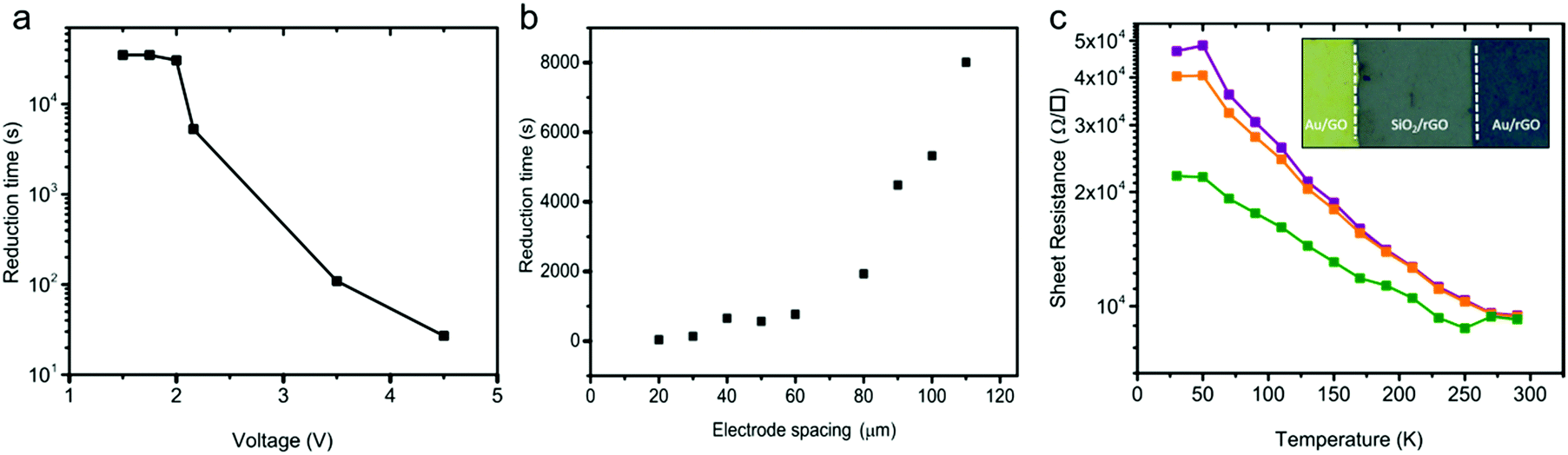 | ||
| Fig. 4 Reduction kinetics and anti-fuse characterization. (a) Reduction time as a function of the applied bias. The electrode spacing was fixed at 50 μm. (b) Reduction time as a function of electrode spacing for an applied bias of +3 V. (c) Temperature dependence of the rGO sheet resistance at various applied biases. The inset shows an optical image of an in-plane anti-fuse where spatial resolution of the area between the Au electrodes is homogeneously reduced. All measurements were performed at an ambient temperature of 23 °C and relative humidity of 45%. | ||
In the next step we applied a fixed bias of 3 V and varied the electrode spacing. The reduction time obtained for different anti-fuses is given in Fig. 4b. The diffusion of H+ ions implicitly shows up in the scaling of the reduction time with electrode spacing as presented in Fig. 4b. The observed trend for the reduction time suggests that the diffusion of H+ ions is the rate-determining step in the reduction of the GO thin-films.
A picture of a GO anti-fuse with a contact spacing of 50 μm is given in the inset of Fig. 4c. The anti-fuse was formed uniformly by applying a fixed bias of 2.16 V. The GO in between the Au electrodes is fully reduced under ambient conditions within 5000 seconds.
To drive the contact resistance, Rc, a series of anti-fuses with co-centric electrode geometry, and different electrode spacings were tested. Four-point probe measurement was performed. The contact resistance was extracted with the circular transfer line method.54 The values of Rc amount to 7 ± 2 kΩ μm, which is comparable to those obtained for transferred CVD graphene, indicating the formation of a good ohmic contact between the rGO film and Au electrodes.
To characterize the conduction mechanism and to estimate the activation energy, Ea, temperature dependent conductivity measurements were carried out under high vacuum conditions at 1 × 10⁻⁶ mbar. The sheet resistance extracted at three bias levels of 40 mV, 400 mV and 4 V is presented as a function of temperature between 30 K and 290 K in Fig. 4c. The sheet resistance amounts to typically 104 Ω □−1 at 290 K and increases monotonically to ∼5 × 10⁴ Ω □−1 as the temperature decreases to 30 K. The conductivity of the rGO films shows an activation energy of 12 ± 5 meV. Observation of a low activation energy is indicative of a highly conductive rGO film. Previous works have reported strongly temperature dependent charge transport and therefore have suggested a hopping transport mechanism with large activation energies that were ascribed to the large number of defects present in the rGO films.44,55,56 Here, the observed weak temperature dependence of the conductivity down to 30 K indicates a high degree of reduction in rGO.
Conclusion
We have presented the spatially resolved solid-state reduction of graphene oxide thin-films. The reduction is based on an electrochemical process that is driven by electrolysis of ambient water (humidity) at the anode. The reduction is initiated at the cathode, upon diffusion of protons. Reduced graphene oxide shows a one-dimensional dendritic growth. The spatially resolved re-establishment of the conductivity by applying a constant DC bias on the electrodes is similar to an anti-fuse and interconnect formation procedure in the microelectronic industry. We have shown that the formation of spatially resolved reduced graphene oxide thin-films is influenced by two factors viz. applied bias, and humidity. Biases larger than 2 V and humidity above 30% are required to form homogeneously reduced graphene oxide thin-films. The diffusion of protons determines the reduction time of the thin-films. Application of spatially resolved rGO could be an economical replacement particularly interesting for vias (vertical interconnect). Furthermore, the conclusive demonstration that the reduction process is irreversible and driven by voltage clarifies the ambiguities regarding the reported enhanced conductivities in the literature.Author contributions
MCMM and KA devised the experiment. MCMM, JH, and NGG performed majority of the electrical measurements and optical imaging. GG performed SEM. RB performed AFM. HL carried out XPS. MCMM, KM, DMdL, and KA worked out the reduction mechanism. All authors have commented on the results, and co-wrote the manuscript. KA supervised the work.Conflicts of interest
The authors declare no competing financial interest.Acknowledgements
M. C. M.-M. acknowledges Gobierno Vasco, Dpto. Industria, Innovación, Comercio y Turismo under the ELKARTEK Program (Grant No. KK-2017/00012) and Dr A. Seifert and Dr M. Knez for letting her to use their laboratory facilities at CIC nanoGUNE. Nerea Gil-Gonzalez was supported by a PhD fellowship from the University of Navarra. K. A. acknowledges the Alexander von Humboldt Foundation for the funding provided in the framework of the Sofja Kovalevskaja Award, endowed by the Federal Ministry of Education and Research, Germany. We gratefully acknowledge financial support from the Max Planck Institute for Polymer Research. The authors thank H. Burg and H. J. Menges for the AFM and scanning Raman measurements. Open Access funding provided by the Max Planck Society.References
- D. A. Stewart and K. A. Mkhoyan, in Graphene Nanoelectronics: Metrology, Synthesis, Properties and Applications, ed. H. Raza, Springer, Berlin Heidelberg, 2012, pp. 435–464 Search PubMed.
- S. Pei and H.-M. Cheng, Carbon, 2012, 50, 3210 CrossRef.
- K. Parvez, R. Li, S. R. Puniredd, Y. Hernandez, F. Hinkel, S. Wang, X. Feng and K. Müllen, ACS Nano, 2013, 7, 3598 CrossRef PubMed.
- J. Yang, J.-W. Kim and H. S. Shin, Adv. Mater., 2012, 24, 2299 CrossRef PubMed.
- X. Wang, L. Zhi, N. Tsao, Ž. Tomović, J. Li and K. Müllen, Angew. Chem., Int. Ed., 2008, 47, 2990 CrossRef PubMed.
- G. Eda, G. Fanchini and M. Chhowalla, Nat. Nanotechnol., 2008, 3, 270 CrossRef PubMed.
- K.-G. Zhou, K. S. Vasu, C. T. Cherian, M. Neek-Amal, J. C. Zhang, H. Ghorbanfekr-Kalashami, K. Huang, O. P. Marshall, V. G. Kravets, J. Abraham, Y. Su, A. N. Grigorenko, A. Pratt, A. K. Geim, F. M. Peeters, K. S. Novoselov and R. R. Nair, Nature, 2018, 559, 236 CrossRef PubMed.
- H. Feng, R. Cheng, X. Zhao, X. Duan and J. Li, Nat. Commun., 2013, 4, 1539 CrossRef PubMed.
- K. Parvez, Z.-S. Wu, R. Li, X. Liu, R. Graf, X. Feng and K. Müllen, J. Am. Chem. Soc., 2014, 136, 6083 CrossRef PubMed.
- S. Yang, S. Brüller, Z.-S. Wu, Z. Liu, K. Parvez, R. Dong, F. Richard, P. Samorì, X. Feng and K. Müllen, J. Am. Chem. Soc., 2015, 137, 13927 CrossRef PubMed.
- H. A. Becerril, J. Mao, Z. Liu, R. M. Stoltenberg, Z. Bao and Y. Chen, ACS Nano, 2008, 2, 463 CrossRef PubMed.
- Z.-S. Wu, W. Ren, L. Gao, B. Liu, C. Jiang and H.-M. Cheng, Carbon, 2009, 47, 493 CrossRef.
- S. Stankovich, D. A. Dikin, R. D. Piner, K. A. Kohlhaas, A. Kleinhammes, Y. Jia, Y. Wu, S. T. Nguyen and R. S. Ruoff, Carbon, 2007, 45, 1558 CrossRef.
- S. Stankovich, R. D. Piner, X. Chen, N. Wu, S. T. Nguyen and R. S. Ruoff, J. Mater. Chem., 2006, 16, 155 RSC.
- V. C. Tung, M. J. Allen, Y. Yang and R. B. Kaner, Nat. Nanotechnol., 2009, 4, 25 CrossRef PubMed.
- M. Alanyalıoğlu, J. J. Segura, J. Oró-Solè and N. Casañ-Pastor, Carbon N. Y., 2012, 50, 142 CrossRef.
- Z. Wang, X. Zhou, J. Zhang, F. Boey and H. Zhang, J. Phys. Chem. C, 2009, 113, 14071 CrossRef.
- S. Y. Toh, K. S. Loh, S. K. Kamarudin and W. R. W. Daud, Chem. Eng. J., 2014, 251, 422 CrossRef.
- M. Zhou, Y. Wang, Y. Zhai, J. Zhai, W. Ren, F. Wang and S. Dong, Chem. – Eur. J., 2009, 15, 6116 CrossRef PubMed.
- R. Lanche, L. E. Delle, M. Weil, X. T. Vu, V. Pachauri, W. M. Munief, P. Wagner and S. Ingebrandt, Phys. Status Solidi, 2013, 210, 968 CrossRef.
- K. V. Sankar and R. Kalai Selvan, Carbon, 2015, 90, 260 CrossRef.
- S. J. An, Y. Zhu, S. H. Lee, M. D. Stoller, T. Emilsson, S. Park, A. Velamakanni, J. An and R. S. Ruoff, J. Phys. Chem. Lett., 2010, 1, 1259 CrossRef.
- J. M. Mativetsky, E. Treossi, E. Orgiu, M. Melucci, G. P. Veronese, P. Samorì and V. Palermo, J. Am. Chem. Soc., 2010, 132, 14130 CrossRef PubMed.
- J. M. Mativetsky, A. Liscio, E. Treossi, E. Orgiu, A. Zanelli, P. Samorì and V. Palermo, J. Am. Chem. Soc., 2011, 133, 14320 CrossRef PubMed.
- J. M. Mativetsky, M. Palma and P. Samorì, in STM and AFM Studies on (Bio)molecular Systems: Unravelling the Nanoworld, ed. P. Samorì, Springer, Berlin Heidelberg, 2008, pp. 157–202 Search PubMed.
- D. den Boer, J. G. Weis, C. A. Zuniga, S. A. Sydlik and T. M. Swager, Chem. Mater., 2014, 26, 4849 CrossRef.
- A. C. Faucett and J. M. Mativetsky, Carbon, 2015, 95, 1069 CrossRef.
- H. H. Gürel and S. Ciraci, J. Phys.: Condens. Matter, 2013, 25, 435304 CrossRef PubMed.
- H. Seo, S. Ahn, J. Kim, Y.-A. Lee, K.-H. Chung and K.-J. Jeon, Sci. Rep., 2014, 4, 5642 CrossRef PubMed.
- P. Yao, P. Chen, L. Jiang, H. Zhao, H. Zhu, D. Zhou, W. Hu, B.-H. Han and M. Liu, Adv. Mater., 2010, 22, 5008 CrossRef PubMed.
- H. F. Teoh, Y. Tao, E. S. Tok, G. W. Ho and C. H. Sow, Appl. Phys. Lett., 2011, 98, 1 CrossRef.
- M. Rogala, P. J. Kowalczyk, P. Dabrowski, I. Wlasny, W. Kozlowski, A. Busiakiewicz, S. Pawlowski, G. Dobinski, M. Smolny, I. Karaduman, L. Lipinska, R. Kozinski, K. Librant, J. Jagiello, K. Grodecki, J. M. Baranowski, K. Szot and Z. Klusek, Appl. Phys. Lett., 2015, 106, 263104 CrossRef.
- Y. Yao, X. Chen, J. Zhu, B. Zeng, Z. Wu and X. Li, Nanoscale Res. Lett., 2012, 7, 363 CrossRef PubMed.
- O. Ö. Ekiz, M. Ürel, H. Güner, A. K. Mizrak and A. Dâna, ACS Nano, 2011, 5, 2475 CrossRef PubMed.
- A. C. Pearson, S. Jamieson, M. R. Linford, B. M. Lunt and R. C. Davis, Nanotechnology, 2013, 24, 135202 CrossRef PubMed.
- B. C. de Brito, E. C. P. Smits, P. A. van Hal, T. C. T. Geuns, B. de Boer, C. J. M. Lasance, H. L. Gomes and D. M. de Leeuw, Adv. Mater., 2008, 20, 3750 CrossRef.
- (a) L. Rojo, I. Castro-Hurtado, M. C. Morant-Miñana, G. G. Mandayo and E. Castaño, CrystEngComm, 2014, 16, 6033 RSC; (b) L. Rojo, I. Castro-Hurtado, M. C. Morant-Miñana, G. G. Mandayo and E. Castaño, CrystEngComm, 2015, 17, 1597 RSC.
- J. S. Mehta, A. C. Faucett, A. Sharma and J. M. Mativetsky, J. Phys. Chem. C, 2017, 121, 16584 CrossRef.
- H. F. Teoh, Y. Tao, E. S. Tok, G. W. Ho and C. H. Sow, Appl. Phys. Lett., 2012, 112, 064309 Search PubMed.
- D. A. Sokolov, Y. V. Morozov, M. P. McDonald, F. Vietmeyer, J. H. Hodak and M. Kuno, Nano Lett., 2014, 14, 3172 CrossRef PubMed.
- A. C. Ferrari and J. Robertson, Phys. Rev. B: Condens. Matter Mater. Phys., 2000, 61, 14095 CrossRef.
- M. M. Lucchese, F. Stavale, E. H. M. Ferreira, C. Vilani, M. V. O. Moutinho, R. B. Capaz, C. A. Achete and A. Jorio, Carbon, 2010, 48, 1592 CrossRef.
- N. Lin, D. Payer, A. Dmitriev, T. Strunskus, C. Wöll, J. V. Barth and K. Kern, Angew. Chem., Int. Ed., 2005, 44, 1488 CrossRef PubMed.
- R. Y. N. Gengler, D. S. Badali, D. Zhang, K. Dimos, K. Spyrou, D. Gournis and R. J. D. Miller, Nat. Commun., 2013, 4, 2560 CrossRef PubMed.
- C. Shen, I. Cebula, C. Brown, J. Zhao, M. Zharnikov and M. Buck, Chem. Sci., 2012, 3, 1858 RSC.
- I. Cebula, H. Lu, M. Zharnikov and M. Buck, Chem. Sci., 2013, 4, 4455 RSC.
- H. Aitchison, H. Lu, M. Zharnikov and M. Buck, J. Phys. Chem. C, 2015, 119, 14114 Search PubMed.
- D. V. Yang, A. Velamakanni, G. Bozoklu, S. Park, M. Stoller, R. D. Piner, S. Stankovich, I. Jung, D. A. Field, C. A. Ventrice and R. Ruoff, Carbon, 2009, 47, 145 CrossRef.
- A. Ganguly, S. Sharma, P. Papakonstantinou and J. Hamilton, J. Phys. Chem. C, 2011, 115, 17009 CrossRef.
- C. Mattevi, G. Eda, S. Agnoli, S. Miller, K. A. Mkhoyan, O. Celik, D. Mastrogiovanni, G. Granozzi, E. Garfunkel and M. Chhowalla, Adv. Funct. Mater., 2009, 19, 2577 CrossRef.
- (a) H. Ji, X. Zhao, Z. Qiao, J. Jung, Y. Zhu, Y. Lu, L. L. Zhang, A. H. MacDonald and R. S. Ruoff, Nat. Commun., 2014, 5, 1 Search PubMed; (b) X. Chen, D. Akinwande, K. J. Lee, G. F. Close, S. Yasuda, B. C. Paul, S. Fujita, J. Kong and H. S. P. Wong, IEEE Trans. Electron Devices, 2010, 57, 3137 Search PubMed.
- J. K. Nørskov, T. Bligaard, A. Logadottir, S. Bahn, L. B. Hansen, M. Bollinger, H. Bengaard, B. Hammer, Z. Sljivancanin, M. Mavrikakis, Y. Xu, S. Dahl and C. J. H. Jacobsen, J. Catal., 2002, 209, 275 CrossRef.
- J. Rossmeisl, A. Logadottir and J. K. Nørskov, Chem. Phys., 2005, 319, 178 CrossRef.
- K. Asadi, E. C. Timmering, T. C. T. Geuns, A. Pesquera, A. Centeno, A. Zurutuza, J. H. Klootwijk, P. W. M. Blom and D. M. de Leeuw, ACS Appl. Mater. Interfaces, 2015, 7, 9429 CrossRef PubMed.
- I. Jung, D. A. Dikin, R. D. Piner and R. S. Ruoff, Nano Lett., 2008, 8, 4283 CrossRef PubMed.
- C. Gómez-Navarro, R. T. Weitz, A. M. Bittner, M. Scolari, A. Mews, M. Burghard and K. Kern, Nano Lett., 2007, 7, 3499 CrossRef PubMed.
Footnote |
| † Electronic supplementary information (ESI) available. See DOI: 10.1039/c8mh00895g |
| This journal is © The Royal Society of Chemistry 2018 |