
 Open Access Article
 This Open Access Article is licensed under a
 Creative Commons Attribution 3.0 Unported Licence
Hard-magnetic cell microscaffolds from electroless coated 3D printed architectures†
Roberto
Bernasconi
 *a,
Federico
Cuneo
a,
Elena
Carrara
a,
George
Chatzipirpiridis
b,
Marcus
Hoop
b,
Xiangzhong
Chen
b,
Bradley J.
Nelson
b,
Salvador
Pané
b,
Caterina
Credi
c,
Marinella
Levi
c and
Luca
Magagnin
*a
*a,
Federico
Cuneo
a,
Elena
Carrara
a,
George
Chatzipirpiridis
b,
Marcus
Hoop
b,
Xiangzhong
Chen
b,
Bradley J.
Nelson
b,
Salvador
Pané
b,
Caterina
Credi
c,
Marinella
Levi
c and
Luca
Magagnin
*a
aDipartimento di Chimica, Materiali e Ingegneria Chimica Giulio Natta, Politecnico di Milano, Via Mancinelli 7, 20131, Milano, Italy. E-mail: roberto.bernasconi@polimi.it; luca.magagnin@polimi.it
bMulti-Scale Robotics Lab, Institute of Robotics and Intelligent Systems, ETH Zurich, Tannenstrasse 3, 8092, Zurich, Switzerland
cDipartimento di Chimica, Materiali e Ingegneria Chimica Giulio Natta, Politecnico di Milano, Piazza Leonardo da Vinci 32, 20133, Milano, Italy
First published on 18th May 2018
Abstract
The combination of 3D printing and wet metallization is a promising methodology for the manufacturing of functional microdevices able to carry out biomedical tasks in vivo. Following this approach, prototypical cell scaffolds are successfully manufactured in the present work. Functional layers are sequentially deposited employing electroless metallization on stereolitography 3D printed moveable structures. Final devices are characterized and magnetically actuated in a precise way using a novel rolling motion approach, which allows for a superior control over speed and position. From the living cells compatibility point of view, the scaffolds show good biocompatibility with fibroblasts after the application of a gold layer.
Conceptual insightsIn this work, we combine for the first time 3D printing and wet metallization for the fabrication of complex multifunctional magnetically driven microscaffolds for targeted cell delivery applications. An all-wet, versatile and costless metallization approach is developed to impart both semi-hard magnetic properties and biocompatibility to the microscaffolds, demonstrating thus its versatility for providing different functionalities on the same device. The use of hard-magnetic materials can be significantly advantageous for the manipulation of microdevices, as these materials can retain magnetization after being subject to a magnetic field. These magnetic memory attributes of hard-magnetic materials can be exploited to program the easy magnetization axis of the device. In this manuscript, cylindrical microscaffolds are pre-magnetized perpendicularly to their long axis to achieve rolling locomotion under the application of rotating magnetic fields. Control over the speed in different fluids and actuation of the microscaffolds along different trajectories are successfully demonstrated. This study represents a significant advance in the manufacturing of magnetically driven biomedical small-scale devices. |
The quest for minimally invasive therapeutic technologies has been one of the main trends in the biomedical arena during the last two decades.1 Conventional treatments, which involve systemic administration of drugs or surgery, carry more side effects, discomfort for patients or longer recovery times. Many of these drawbacks can be significantly reduced by limiting the invasiveness of therapies. While minimally invasive techniques are already in use,1 more innovative ones are currently under development. The use of remotely controlled micro and nanodevices – also known as micro- and nanorobots – is a promising approach for future high-precision minimally invasive therapies, such as targeted delivery of drugs2 and stem cells,3,4 localized surgery,5,6 or diagnosis.4 To this end, many efforts have been made to engineer small-scale machines that can be wirelessly navigated in liquids. The locomotion of these devices has been one of the most investigated aspects by researchers during the last decade. Moving through fluids is challenging for a small-scale device because viscous forces dominate over inertial forces. The ratio between these two types of forces is given by the Reynolds number Re. Microorganisms, such as bacteria or parasites, are characterized by Re in the range of 10−1–10−4. The immediate consequence of swimming at low Re is that reciprocal mechanisms for swimming will not result in forward motion at micro- and nanoscales in Newtonian fluids. This is known as Purcell's scallop theorem.7 Hence, to be able to swim in these conditions, microorganisms have adopted non-reciprocal mechanisms, which imply the use of appendages such as flagella or cilia.
In the field of small-scale machines, two main strategies have been proposed to confer motion to these devices: (a) using chemical fuels that are in the surrounding fluid;8,9 (b) using an external source of energy such as light,10 ultrasounds11 or magnetic fields.12,13 The first implies that a chemical will react with the device's surface, for instance, a catalyst, and the product or products of this reaction will cause the propulsion of the device. The second strategy consists of using materials that are responsive to an external energy input. Among the possible approaches, the use of magnetic fields is a promising way to wirelessly control the locomotion of micro- and nanodevices especially for in vivo biomedical applications.14 Magnetic fields are already in use for clinical applications and diagnosis. Advantageously, magnetic fields can penetrate human tissues and they can be used in a wide range of conditions. Different types of applied magnetic patterns have been proposed to move micro- and nanomachines according to their shape: magnetic field gradients,15 oscillating,16 or rotating magnetic fields.17–22 Such patterns can be easily applied, even in vivo, using existing state-of-the-art technologies.23 Among all these possibilities, an interesting way to propel magnetic structures consists of rolling or tumbling them on surfaces by applying rotating magnetic fields. For example, Chatzipirpiridis et al. have recently shown that hard-magnetic microtubes magnetized perpendicularly to their long axis can roll on surfaces when they are subject to rotating magnetic fields.24 Choi and co-workers have shown that magnetic 3D porous scaffold structures fabricated by two-photon lithography and e-beam evaporation can successfully roll on surfaces and act as conveyors of cells.25 Pieters et al.26 have also investigated the rolling locomotion of cuboid microstructures containing soft-magnetic micropillars, known as RodBots. The microdevices were used to transport protein crystals by means of the vortices generated during the rolling of the device. Bi et al.27 have recently described the fabrication and manipulation of magnetic tumbling robots, which can move in multiple environments and complex terrains. The microdevices were manufactured using a two-step photolithography process and were made of SU-8 composites containing aligned hard-magnetic NdFeB microparticles.
While there is a wealth of examples of magnetic surface micro- and nanowalkers,28–31 many developments are still required to produce optimal devices, for instance, in terms of their magnetic materials. Electrochemical processing methodologies, such as electroless or electrodeposition, offer a wide range of possibilities regarding the integration of different materials in micro- and nanodevices. Electroless deposition, in particular, is highly convenient from the cost and simplicity point of view to deposit metallic layers on non-conductive surfaces. Magnetic and functional layers can be deposited in a more convenient way with respect to other techniques like e-beam evaporation or sputtering. From the applicative point of view, Pumera and co-workers have recently emphasized the versatility of electrochemistry in the production of micro- and nanomachines.32,33
In this work, we wanted to investigate the potential of electroless metallization to coat 3D-printed porous scaffolds with a hard-magnetic material. The 3D structures are fabricated by means of stereolithography (SLA). SLA is based on the polymerization of a photocurable resin using a UV laser source, computer-controlled by galvano-mirrors.34 This technology is not able to reach ultrasmall dimensions like two-photon polymerization, but it's ideal for feature sizes in the hundreds of micrometers range. Due to the limited investment cost for the equipment and to the lack of a clean room, SLA is the best choice to allow a low cost approach to the manufacturing of microdevices that does not require considerably small dimensions.35 To metallize the 3D polymeric structures, an electrolyte to produce cobalt–nickel–phosphorus (CoNiP) films was selected. CoNiP alloys exhibit semi-hard-magnetic properties, which can be easily tuned by modifying the deposition parameters.36,37 To increase the biocompatibility characteristics of the devices, the surface of the CoNiP top layer was covered with gold by means of the electroless nickel-immersion gold technique (ENIG), a process usually employed in the electronic manufacturing field.38
In the first manufacturing step, microscaffolds were 3D printed using stereolithography. According to the specifications provided by the manufacturer (DWS systems), the stereolithography machine employed is able to focus a beam spot down to 22 μm. This parameter, mainly affecting the lateral resolution, is however not representative of the actual minimum SLA-printable feature size, which is strictly related to the vertical resolution, in terms of thickness of single cured layer, that in turn is dependent on both the Z-platform movement and on the resin-laser interaction.39 While the former is dependent on the specific machine exploited (10–100 μm with our apparatus), the latter could be quantified by the critical energy Ec and the penetration depth Dp defined as the required energy dose to cross-link the resin and the length of penetration of the laser within the resin, respectively, for a single-line scan. As a result, achieving higher resolution of built objects requires minimizing the penetration depth so that thinner slices can be fabricated and stacked together while small critical energies enable fast polymerization and speed up the whole printing technologies. To tailor the penetration depth and to obtain very thin polymerized layers, highly absorbing resins need to be designed to confine the laser radiance at the surface of the reactive medium.40 To this end, organic and inorganic additives, differently affecting the photopolymerization process by absorbing photons, scavenging radicals or inducing scattering, can be mixed to the basic formulation of the photopolymers.
Finally, micrometric samples were successfully printed within 30 minutes (Fig. 1b), thus highlighting the huge impact that 3D printing processes have on decreasing the overall time of the microfabrication process respect to the time-consuming standard lithographic-based technologies. Microdevices were printed in two sizes, namely L (large) and S (Small). L samples are characterized by a 4.5 mm length, while S samples are 3 mm long. Nominal dimensions of the devices are fully described in Fig. S1 and Table S1 (ESI†). Optical images of the samples, visible in Fig. S2 (ESI†), certify the good dimensional adherence of the printed samples to the 3D model. SEM analysis, reported in Fig. 2a, revealed the excellent physical integrity of the printed microdevices showing fully interconnected pore networks as well as a well-defined and repetitive architecture with the smallest features almost coinciding with the printing resolution. The sidewall of the samples is not smooth but is characterized by a micron-sized wavy structure as a result of a layer-by-layer construction typical of a SLA process.
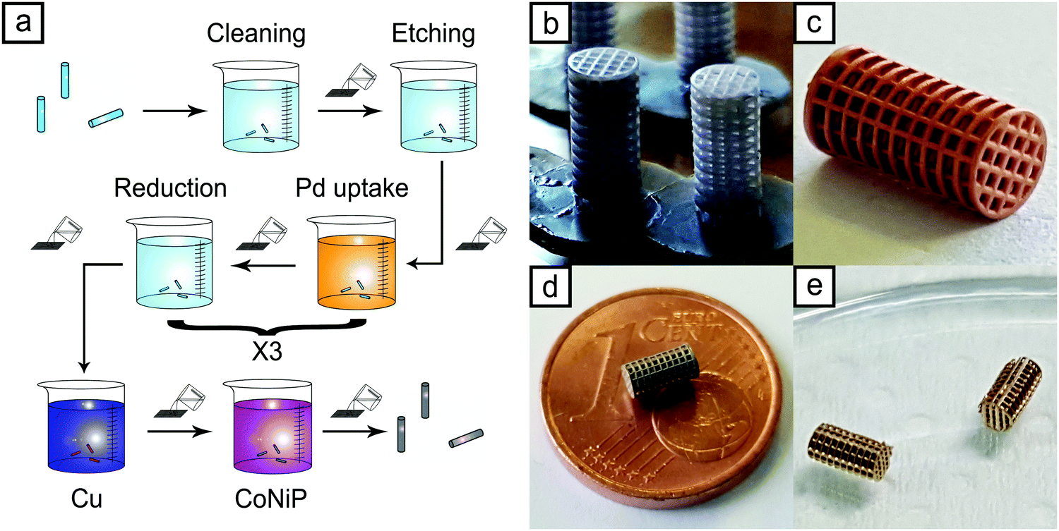 | ||
| Fig. 1 Electroless metallization process (a); visual appearance of the L scaffolds as printed (b) and after being coated with Cu (c) and CoNiP (d); ENIG Au metallized S samples (e). | ||
 | ||
| Fig. 2 SEM image of a L microdevice metallized with Cu/CoNiP/NiP/Au ((a) scale bar = 100 μm); particular of a L sample metallized only with Cu and CoNiP ((b) scale bar = 10 μm); particular of a S sample metallized with Cu/CoNiP/NiP/Au ((c) scale bar = 60 μm); particular of the same S sample ((d) scale bar = 20 μm); XRD of the CoNiP plated on a planar Cu substrate for 30 minutes (e); AFM analysis of the surface of a L sample ((f) scale bar = 500 μm). | ||
After 3D printing, samples were metallized, but prior to this step the most relevant properties of the deposited metallic layers were investigated to evaluate their use as functional layers on the printed microdevices. Such properties, together with plating speed during metallization, are strongly connected to the relatively low temperature used for their deposition. A temperature below or equal to 45 °C is necessary due to the physical properties of the DL260 resin, which present a glassy transition around 50 °C.41 Conversely, temperature should be as high as possible to allow high deposition rate. For these reasons, a temperature slightly lower than 50 °C was selected as optimal.
The first layer applied on the surface of the resin is made of Cu, which must provide good adhesion and improved activation for the following CoNiP layer. It was in fact observed that the direct application of CoNiP on the resin at relatively low temperature (45 °C) resulted in low adhesion, activation problems for the electroless plating of the surface and in general an insufficient morphological quality of the alloy. The use of an intermediate Cu coating was found to be a good solution for these problems. Properties of the first Cu layer, deposited on DL260, have been investigated in a previous work.41 The mean thickness of the coating, as a consequence of the low temperature used during the deposition, was found to be around 400 nm. Adhesion to the substrate, qualitatively evaluated by means of a peel test, was found to be good.
The second layer applied on the surface is made of CoNiP. This material works as active material for the actuation of the microdevices. Considering the actuation mechanism selected,24 the main desired properties for this layer are high magnetic coercivity and good remanence, as the devices must not lose their magnetization upon exposure to the actuation field. Coercivities higher than 200 Oe are preferred, since this value should ensure a reasonable resistance to demagnetization during magnetic manipulation. A secondary property imparted by the CoNiP layer is mechanical resistance. Due to the presence of P in the alloy, hardness and elastic modulus of CoNiP are typically high. This is beneficial for the devices, which results in an improvement of the mechanical properties after the application of the CoNiP. 4.5 μm of CoNiP were applied on the Cu plated resin. Its composition, analyzed by EDS, is as follows: 71 wt% Co, 26 wt% Ni and 3 wt% P.
Magnetic properties of the CoNiP layer were evaluated using VSM. Fig. S4 (ESI†) shows the results obtained depositing CoNiP on a planar Cu sheet, while Fig. 3a reports the results of the same analysis performed on a microdevice already metallized with Cu. In the case of the planar sample, an “in plane” direction indicates a magnetization parallel to the plane, while an “out of plane” direction is indicative of a magnetization perpendicular to the plane. In the case of the device, a “parallel” direction indicates a magnetization along the long axis of the cylinder, while a “perpendicular” direction indicates a magnetization perpendicular to such axis. Magnetization was normalized with respect to saturation magnetization.
 | ||
| Fig. 3 Magnetic hysteresis curves obtained via VSM for CoNiP on a L microdevice (a); schematics of the actuation mechanism (b); circular pattern actuation of an L device (c); S shaped actuation of an S device (d); rotation of an S device (e). | ||
The first hysteresis curve, obtained from a planar CoNiP layer, is characterized by a strong anisotropy between the two magnetization directions. This phenomenon is common in electroless deposited magnetic materials and it is connected to the internal structure of the coating, which typically presents a columnar structure with grains elongated in the growth direction of the layer. Concentration gradients for the various elements may be present as well, with the final result of a significant difference between the in plane and the out of plane directions. The in plane and out of plane coercivity values were 780 Oe and 618 Oe, respectively. Remanence values were 218 emu cm−3 in plane and 81 emu cm−3 out of plane. Squareness was equal to 0.202 in the in plane direction and to 0.083 in the out of plane orientation. Due to the already discussed microstructural anisotropy of the film, all the values are lower for the out of plane direction. Coercivity values for the alloy are indicative of a semi-hard material and are high enough to retain efficiently a permanent magnetization during rolling actuation.
The microdevices described in the text are however not planar. They are on the contrary tridimensional objects, where the metallic layer can exhibit many different orientations. It is reasonable thus to expect less anisotropy connected to microstructural inhomogeneity and more related to the shape of the sample. Moreover, thickness of the metallic layer is higher in the case of the microdevices than the planar sample described. This aspect is clearly visible in Fig. 3a, where the VSM analysis of a device is presented. Magnetic properties along the two perpendicular directions are similar. Minor differences between the two curves are mainly due to the shape anisotropy of the sample. Remanence values are 140 emu cm−3 in the parallel direction and 96 emu cm−3 in the perpendicular direction. Squareness is 0.116 in the perpendicular direction and 0.168 in the parallel orientation. Coercivity values are comparable with the ones obtained from the planar sample. Such values are: 632 Oe along the parallel direction and 606 Oe along the perpendicular direction. These values are similar to the ones obtained from the planar sample in the out of plane direction, implying that the thickness increase between 30 minutes and 3 hours of deposition does not decrease significantly coercivity. This behavior is coherent with existing literature, as typically magnetic properties are constant after roughly 1 μm of thickness of the electroless deposited layer.42,43 Moreover, independency of coercivity from thickness is indicative of the deposition of a good layer from the compositional point of view. It is in fact reasonable to state that composition should be constant along the thickness of the coating, as variations of composition are known to cause strong variations in magnetic properties. Such compositional homogeneity is a consequence of the small dimension and the small quantity of devices prepared in each metallization batch. From four to six samples were metallized in a 200 ml solution, allowing thus a low plating surface to electrolyte volume ratio. The main result of such small ratio is a reduced variation of pH during deposition (pH is a vital parameter for compositional control of electroless deposited CoNiP37). To avoid compositional inhomogeneity in the samples, it is convenient to keep as low as possible the number of devices plated with respect to the volume of solution employed.
To better understand magnetic properties, the microstructure of CoNiP plated on a planar substrate for 30 minutes was evaluated using XRD. The result obtained is visible in Fig. 2e. According to the XRD graph visible in Fig. 2e, the CoNiP alloy is composed of a microcrystalline fcc Ni-rich phase and of a hcp Co-rich phase. This structure has already been reported in the past44 in the case of chemically deposited CoNiP. According to the theoretical positions and relative intensities of the Ni peaks (JCPDS card 04-0850), the Ni-rich phase is prevalently oriented along the [111] crystallographic direction and has relatively large crystallites. On the contrary, the Co-rich phase (JCPDS card 05-0727) is characterized by a nanocrystalline structure (as easily assumed from the broadening of the [101] peak, which is the most intense for hcp Co). Due to its microstructure, it is probable that the Co phase is the most P rich. As already discussed by Homma et al.,44 these two phases possess some orientation in the CoNiP grains. Such orientation is the origin of the magnetocrystalline anisotropy observed in Fig. 3a.
Another important effect of the addition of a CoNiP layer to the structure of the microdevices is the increase in mechanical properties and shape stability. By performing microindentation on a CoNiP section, an elastic modulus of 139 GPa was estimated. For comparison, the elastic modulus of the DL260 resin was determined with the same technique and it was found to be two orders of magnitude lower (1.82 GPa). The final structure obtained, composed of a DL260 resin core and a metal overlayer, presents mechanical properties analogous to a composite.
NiP was deposited as the third metallic layer to allow displacement deposition of gold. ENIG deposition was attempted directly on CoNiP, but the results were found to be not acceptable in terms of surface appearance and layer porosity. NiP was therefore deposited on CoNiP according to a methodology already used.41 Final thickness was found to be 1.1 μm and the phosphorus content to be 2.5 wt%.
Finally, gold was deposited on NiP from a commercial ENIG solution. Such solution should be used in the 80–90 °C temperature range for at least 30 minutes to achieve a good quality ENIG layer. DL260 resin, however, cannot withstand temperatures higher than 45–50 °C without deforming, and for this reason the temperature was limited to 45 °C. At such low temperature the kinetic for gold displacement is considerably slower. For this reason, immersion time in the ENIG solution was prolonged to 4 h. Two samples, obtained at 30 minutes and 3 h immersion time, were used for the biocompatibility tests to show the influence of the final gold layer uniformity on the functionality of the devices. Typical final Au thickness after ENIG is in the range 80–120 nm. If necessary, Au thickness can be further increased by using gold electroless deposition.45
Once the properties of the metallic layer employed were determined, the devices were removed from the printing supports and subjected to the metallization process described previously. Fig. 1 represents the visual appearance of the samples after each metallization step (after copper in Fig. 1c, after CoNiP in Fig. 1d and after ENIG in Fig. 1e). Conversely, Fig. S5 (ESI†) depicts the appearance of some L samples coated with CoNiP and ENIG.
As expected from the results obtained in the past on DL260, metallization was found to be adherent and homogeneous on the surface of the samples. It is however impossible to determine, only with a visual inspection, if the metallization is complete also in the inner zone of the scaffold. To check the uniformity of the metal layer inside the structure, a cross section of an L device was obtained and observed using optical microscopy. The result is visible in Fig. S6 (ESI†).
As visible in the composite section presented, deposition is uniform also inside the device. Electroless deposition is able to deposit metallic layer in high aspect ratio micrometric trenches, thus it is reasonable to observe a good uniformity in devices presenting pores in the order of hundreds of micrometers. To confirm what observed qualitatively, thickness was evaluated in three different points (A, B and C in Fig. S6, ESI†) starting from a region close to the outer surface of the device and then moving deeper. Thickness was found to be 4.63 μm in zone A, 4.58 μm in zone B and 4.64 μm in zone C, respectively. No significant differences between the three points were therefore observed.
The two kinds of samples, L and S, were observed also with SEM. Fig. 2a and Fig. S7 (ESI†) depict the result obtained. The first important feature extrapolated from Fig. S7 (ESI†) is the difference between the nominal dimensions and the real ones. In particular for the L sample is visible a higher line dimension along the printing direction (that is parallel to the symmetry axis). The circular slices that compose the device present therefore a thickness higher than the lines that connect them. This could be likely ascribed to the laser penetration, as previously explained. The residues of the printing supports are visible on the left in Fig. 2a.
In the case of the S sample (Fig. S7, ESI†), dimensions are more homogeneous. Conversely, a strong edge rounding is present. This effect can be due to the surface tension of the resin, which is more relevant as a consequence of the reduced dimension with respect to L samples, but also to the different printing direction used for S devices. In this case, the printing was performed along a direction perpendicular to the symmetry axis (as visible in Fig. S3, ESI†). Printing supports were therefore placed on the face opposite to the one visible in Fig. S7 (ESI†). Their residues are visible in Fig. 2c.
Fig. 2b and d show different particulars of two samples at two different metallization stages. Fig. 2b shows the typical nodular morphology of the electroless deposited CoNiP layer at the intersection between two printed lines. A CoNiP layer characterized by a good uniformity and compactness uniformly covers the surface. After the ENIG process, morphology is slightly altered (as visible in Fig. 2d). The nucleation of new nuclei (as a consequence of NiP deposition) and the Au displacement deposition changed the appearance of the surface. Fig. 2c and d visually demonstrate that complete metallization of the device was successfully achieved, also in its inner parts. The appearance of the 3D printed surface in Fig. 2c looks different with respect to the zone shown in Fig. S7 (ESI†). Such inhomogeneity is probably due to the effect of printing direction.
Morphology of the gold covered surface is a fundamental parameter to evaluate the functionality of the device. Surface roughness is in fact able to strongly influence cell adhesion on the microrobot. For this reason, surface roughness Ra was evaluated on the final device after the application of the Au layer. AFM was performed on the zone at the intersection between two printed lines, as visible in Fig. 2f. From Fig. 2f, two levels of surface structuring can be observed. The first one is characterized by large nodules coming from the CoNiP layer. These nodules, clearly visible in the SEM analysis (Fig. 2b), are well defined also in the AFM picture. A finer structure can be observed on the surface of the nodules. Such structure is probably a result of the nucleation of a new layer (the NiP used as first step of the ENIG process) coupled with the displacement reaction occurred during gold deposition. The presence of two well defined levels of surface structuring can be also confirmed analyzing surface roughness at different scan sizes. Table 1 reports the results obtained with respect to AFM scan size.
| Scan size (μm) | R a value (nm) |
|---|---|
| 50 × 50 | 350 |
| 20 × 20 | 312 |
| 10 × 10 | 266 |
| 5 × 5 | 119 |
| 2 × 2 | 53 |
As long as scan size is larger than the dimension of the nodules (typically in the range 3–6 μm from SEM and AFM), roughness values are high. This effect is clearly visible in Table 1, where Ra values are roughly comparable down to 10 × 10 μm scan size. At 5 × 5 μm, roughness suddenly drops and at 2 × 2 μm it is one order of magnitude lower than at 50 × 50 μm.
Microscaffolds were actuated employing a rolling mechanism based on the presence of a rotating magnetic field. This method has already been investigated in the past24 and was found to be able to guarantee a good control on speed and direction of the microdevice. Fig. 3b depicts schematically the working principle.
The CoNiP layer present in the device is premagnetized under a strong static magnetic field, produced by a NdFeB permanent magnet. When such field is removed, a residual magnetization M is present. The value of M can be qualitatively evaluated from the hysteresis curve presented in Fig. 3a. When an external field H is applied to the device, M (and consequently the device itself) align according to the direction of H. If H rotates with frequency ω, the final result is a rotation of the device with frequency ω′ and a net forward motion with speed v. ω′ is never perfectly equal to ω due to the resistance of the fluid in which the motion takes place and to rolling friction with the substrate. Therefore the speed of the device is never equal to the theoretical speed. Theoretical speed can be correlated to the diameter of the device by eqn (1).
| v = 2πrω′ | (1) |
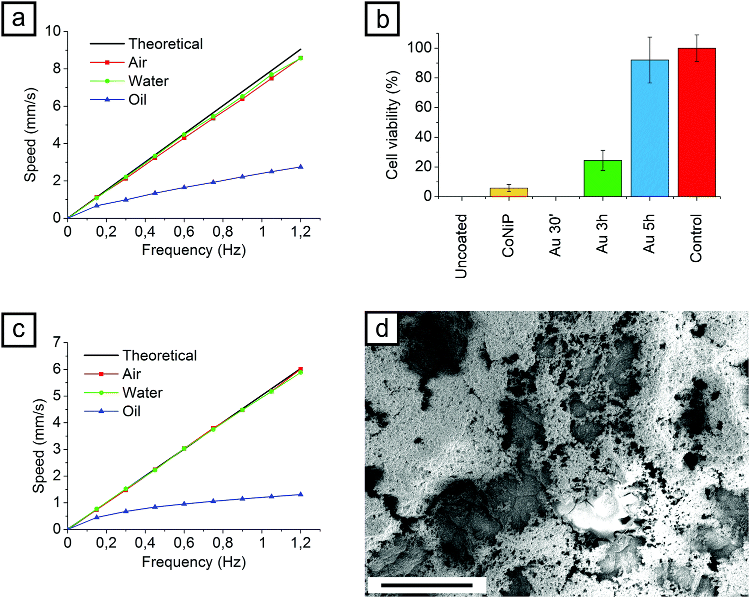 | ||
| Fig. 4 Magnetic field rotation frequency vs. device speed relationship in the case of L (a) and S (c) devices; cell viability after 2 days for microdevices in different production stages (b); surface of the sample Au 30′ after the cell viability test (d). | ||
If the rotation axis of the magnetic field H is changed, the direction of the device can be controlled. Fig. 3c shows a L samples describing with its motion a circular pattern. Direction of the rotation axis was continuously modified from 0° to 360° to achieve such controlled movement. In Fig. 3d a S scaffolds describes a S shaped pattern. In this case the rotation axis was rotated of 90° and subsequently moved back to 0°. The scaffolds can be put in rotation as well by tilting the rotation plane for H of 90° outside the plane (Fig. 3e).
The surface of the scaffolds, as a consequence of the Au layer deposited by the ENIG process, was expected to become biocompatible. Biocompatibility of gold deposited by galvanic displacement has already been reported,46 but only on nanometric features. A biocompatibility test was therefore performed using L samples (Fig. 4b).
As printed and CoNiP plated samples were investigated together with gold plated scaffolds for comparison. Three immersion times in the ENIG bath, 30 minutes (Au 30′), 3 hours (Au 3 h) and 5 hours (Au 5 h) were considered. The DL 260 resin is characterized by a 0% cell viability after 2 days, making it cytotoxic for fibroblasts. Both the CoNiP plated and the Au 30′ samples are cytotoxic as well. The reason for the cell viability lower for the Au 30′ sample than for the CoNiP sample is the porosity of the gold layer. Since gold displacement kinetic is slower at 50 °C, 30 minutes are not enough to obtain a complete coverage of the surface. The coating presents thus a nanometric porosity and the galvanic coupling with the NiP layer underneath results in a strong corrosion. An image of the surface of the sample after the test, showing the gold layer completely damaged, is represented by Fig. 4d.
If the ENIG deposition is prolonged up to 3 h, the surface becomes more biocompatible, as visible in Fig. 4b. Almost complete cell viability (92%) after 2 days can be obtained after 5 hours of immersion in the gold galvanic displacement. After the test (Fig. S8, ESI†), the surface of the devices appears unaltered and similar to the one depicted in Fig. 2c and d.
By increasing plating time in ENIG, surface porosity of the gold layer can be reduced sufficiently to allow good values of cell viability after 2 days.
Conclusions
The possibility to obtain fully functional microrobots combining cost effective manufacturing techniques like stereolithography 3D printing and wet metallization was demonstrated. A cylindrical scaffold structure was successfully printed and subsequently metallized with different functional layers. Semi-hard magnetic properties were achieved depositing an electroless CoNiP layer on the scaffolds. Such layer proved to be sufficiently magnetically hard to program the easy magnetization direction of the device and subsequently enable the devices to roll on surfaces. Control over the speed and position of the scaffolds was demonstrated by applying suitably oriented rotating magnetic fields. Microrobots were capped with an ENIG treatment to impart biocompatibility to the otherwise cytotoxic CoNiP layer. Biocompatibility tests evidenced a good fibroblasts compatibility of the final devices over a time window of two days. The rolling actuated microscaffolds described in the present work constitute potential tools for targeted cell delivery in human body cavities characterized by millimetric diameters, like the digestive apparatus or large blood vessels. Most importantly, they constitute a benchmark that demonstrate the applicability of a novel manufacturing route and of an innovative actuation approach to the realization of functional microdevices.Author contributions
R. Bernasconi and F. Cuneo designed the manufacturing process and metallized the samples, E. Carrara metallized the samples, C. Credi 3D printed the samples, M. Hoop performed biocompatibility tests. G. Chatzipirpiridis, X. Chen, B. J. Nelson, Salvador Pané, M. Levi and L. Magagnin wrote the paper.Conflicts of interest
The authors declare that there are no conflicts of interest for the present paper.Acknowledgements
The work described in the text was carried out in the framework of the interdepartmental laboratory MEMS&3D at Politecnico di Milano, Milano, Italy. The authors would like to acknowledge networking support by the COST Action MP1407 (e-MINDS) and the SBFI Cost Project No. C16.0061 under the frame of this COST Action. They would also like to acknowledge the contribution of S. Bernasconi to the realization of some images present in the text.References
- A. H. Vernon and S. W. Ashley, Atlas of Minimally Invasive Surgical Techniques, Elsevier Health Sciences, 2011 Search PubMed.
- Z. Wu, Y. Wu, W. He, X. Lin, J. Sun and Q. He, Angew. Chem., Int. Ed., 2013, 52, 7000–7003 CrossRef PubMed.
- B. J. Nelson, I. K. Kaliakatsos and J. J. Abbott, Annu. Rev. Biomed. Eng., 2010, 12, 55–85 CrossRef PubMed.
- M. Kim, E. Steager and J. Agung, Microbiorobotics: biologically inspired microscale robotic systems, William Andrew, 2012 Search PubMed.
- K. B. Yesin, Int. J. Rob. Res., 2006, 25, 527–536 CrossRef.
- Z. Wu, T. Li, W. Gao, T. Xu, B. Jurado-Sánchez, J. Li, W. Gao, Q. He, L. Zhang and J. Wang, Adv. Funct. Mater., 2015, 25, 3881–3887 CrossRef.
- E. M. Purcell, Am. J. Phys., 1977, 45, 3–11 CrossRef.
- W. F. Paxton, K. C. Kistler, C. C. Olmeda, A. Sen, S. K. S. Angelo, Y. Cao, T. E. Mallouk, P. E. Lammert and V. H. Crespi, J. Am. Chem. Soc., 2004, 126, 13424–13431 CrossRef PubMed.
- D. Kagan, R. Laocharoensuk, M. Zimmerman, C. Clawson, S. Balasubramanian, D. Kang, D. Bishop, S. Sattayasamitsathit, L. Zhang and J. Wang, Small, 2010, 6, 2741–2747 CrossRef.
- F. Cheng, R. Yin, Y. Zhang, C.-C. Yen and Y. Yu, Soft Matter, 2010, 6, 3447–3449 RSC.
- D. Ahmed, T. Baasch, B. Jang, S. Pane, J. Dual and B. J. Nelson, Nano Lett., 2016, 16, 4968–4974 CrossRef PubMed.
- S. Erni, S. Schürle, A. Fakhraee, B. E. Kratochvil and B. J. Nelson, J. Micro-Bio Robot., 2013, 8, 107–120 CrossRef.
- J. J. Abbott, Z. Nagy, F. Beyeler and B. Nelson, IEEE Robot. Autom. Mag., 2007, 14, 92–103 CrossRef.
- X.-Z. Chen, M. Hoop, F. Mushtaq, E. Siringil, C. Hu, B. J. Nelson and S. Pané, Appl. Mater. Today, 2017, 9, 37–48 CrossRef.
- S. Fusco, M. S. Sakar, S. Kennedy, C. Peters, R. Bottani, F. Starsich, A. Mao, G. A. Sotiriou, S. Pané, S. E. Pratsinis, D. Mooney and B. J. Nelson, Adv. Mater., 2014, 26, 952–957 CrossRef PubMed.
- H. W. Tung, M. Maffioli, D. R. Frutiger, K. M. Sivaraman, S. Pané and B. J. Nelson, IEEE Trans. Robot., 2014, 30, 26–32 CrossRef.
- R. Mhanna, F. Qiu, L. Zhang, Y. Ding, K. Sugihara, M. Zenobi-Wong and B. J. Nelson, Small, 2014, 10, 1953–1957 CrossRef.
- F. Qiu, R. Mhanna, L. Zhang, Y. Ding, S. Fujita and B. J. Nelson, Sens. Actuators, B, 2014, 196, 676–681 CrossRef.
- K. E. Peyer, E. Siringil, L. Zhang and B. J. Nelson, Bioinspiration Biomimetics, 2014, 9, 46014 CrossRef.
- K. E. Peyer, S. Tottori, F. Qiu, L. Zhang and B. J. Nelson, Chem. – Eur. J., 2013, 19, 28–38 CrossRef.
- B. J. Nelson and K. E. Peyer, ACS Nano, 2014, 8, 8718–8724 CrossRef.
- A. W. Mahoney and J. J. Abbott, Appl. Phys. Lett., 2011, 99, 1–4 Search PubMed.
- M. P. Kummer, J. J. Abbott, B. E. Kratochvil, R. Borer, A. Sengul and B. J. Nelson, IEEE Trans. Robot., 2010, 26, 1006–1017 CrossRef.
- G. Chatzipirpiridis, E. Avilla, O. Ergeneman, B. J. Nelson and S. Pane, IEEE Trans. Magn., 2014, 50, 10–12 CrossRef.
- S. Kim, F. Qiu, S. Kim, A. Ghanbari, C. Moon, L. Zhang, B. J. Nelson and H. Choi, Adv. Mater., 2013, 25, 5863–5868 CrossRef.
- R. Pieters, H.-W. Tung, S. Charreyron, D. F. Sargent and B. J. Nelson, in Robotics and Automation (ICRA), 2015 IEEE International Conference on, IEEE, 2015, pp. 4042–4047 Search PubMed.
- C. Bi, M. Guix, B. V. Johnson, W. Jing and D. J. Cappelleri, Micromachines, 2018, 9, 68–85 CrossRef.
- L. Zhang, T. Petit, Y. Lu, B. E. Kratochvil, K. E. Peyer, R. Pei, J. Lou and B. J. Nelson, ACS Nano, 2010, 4, 6228–6234 CrossRef.
- X.-Z. Chen, N. Shamsudhin, M. Hoop, R. Pieters, E. Siringil, M. S. Sakar, B. J. Nelson and S. Pané, Mater. Horiz., 2016, 3, 113–118 RSC.
- X. Chen, M. Hoop, N. Shamsudhin, T. Huang, B. Özkale, Q. Li, E. Siringil, F. Mushtaq, L. Di Tizio and B. J. Nelson, Adv. Mater., 2017, 29, 1605458 CrossRef PubMed.
- F. Mushtaq, A. Asani, M. Hoop, X. Z. Chen, D. Ahmed, B. J. Nelson and S. Pané, Adv. Funct. Mater., 2016, 26, 6995–7002 CrossRef.
- H. Wang and M. Pumera, Chem. Rev., 2015, 115, 8704–8735 CrossRef PubMed.
- J. G. S. Moo, C. C. Mayorga-Martinez, H. Wang, B. Khezri, W. Z. Teo and M. Pumera, Adv. Funct. Mater., 2017, 27, 1604759 CrossRef.
- I. Gibson, D. W. D. W. Rosen and B. Stucker, Additive Manufacturing Technologies: Rapid Prototyping to Direct Digital Manufacturing, Springer, 2009, vol. 54 Search PubMed.
- F. P. W. Melchels, J. Feijen and D. W. Grijpma, Biomaterials, 2010, 31, 6121–6130 CrossRef.
- R. Tarozaite, G. Stalnionis, A. Sudavičius and M. Kurtinaitiene, Surf. Coat. Technol., 2001, 138, 61–70 CrossRef.
- R. Bernasconi, F. Cuneo, C. Credi, M. Levi, A. Lucotti, P. L. Cavallotti and L. Magagnin, ECS Trans., 2017, 75, 43–60 CrossRef.
- B. K. Kim, S. J. Lee, J. Y. Kim, K. Y. Ji, Y. J. Yoon, M. Y. Kim, S. H. Park and J. S. Yoo, J. Electron. Mater., 2008, 37, 527–534 CrossRef.
- P. F. Jacobs, Rapid prototyping & manufacturing: fundamentals of stereolithography, Society of Manufacturing Engineers, 1992 Search PubMed.
- A. Bertsch, P. Bernhard, C. Vogt and P. Renaud, Rapid Prototyp. J., 2000, 6, 259–266 CrossRef.
- R. Bernasconi, C. Credi, M. Tironi, M. Levi and L. Magagnin, J. Electrochem. Soc., 2017, 164, B3059–B3066 CrossRef.
- T. Homma, K. Inoue, H. Asai, K. Ohrui, T. Osaka, Y. Yamazaki and T. Namikawa, J. Magn. Soc. Jpn., 1991, 6, 113–116 CrossRef.
- D. Y. Park, N. V. Myung, M. Schwartz and K. Nobe, Electrochim. Acta, 2002, 47, 2893–2900 CrossRef.
- T. Homma, T. Osaka, Y. Yamazaki and T. Namikawa, Scr. Metall. Mater., 1995, 33, 1569–1573 CrossRef.
- L. Berdondini, P. D. van der Waals, N. F. De Rooij and M. Koudelka-Hep, Sens. Actuators, B, 2004, 99, 505–510 CrossRef.
- C.-W. Hsu, C.-W. Li and G.-J. Wang, RSC Adv., 2014, 4, 12127–12132 RSC.
Footnote |
| † Electronic supplementary information (ESI) available. See DOI: 10.1039/c8mh00206a |
| This journal is © The Royal Society of Chemistry 2018 |