
Surface modification of a hole transporting layer for an efficient perovskite solar cell with an enhanced fill factor and stability†
Mohammad Mahdi
Tavakoli
 *ab,
Rouhollah
Tavakoli
a,
Daniel
Prochowicz
c,
Pankaj
Yadav
d and
Michael
Saliba
*e
*ab,
Rouhollah
Tavakoli
a,
Daniel
Prochowicz
c,
Pankaj
Yadav
d and
Michael
Saliba
*e
aDepartment of Materials Science and Engineering, Sharif University of Technology, 14588 Tehran, Iran
bDepartment of Electrical Engineering and Computer Science, Massachusetts Institute of Technology, Cambridge, MA, USA. E-mail: mtavakol@mit.edu
cInstitute of Physical Chemistry, Polish Academy of Sciences, Kasprzaka 44/52, 01-224 Warsaw, Poland
dDepartment of Solar Energy, School of Technology, Pandit Deendayal Petroleum University, Gandhinagar-382 007, Gujarat, India
eAdolphe Merkle Institute, Chemins des Verdiers 4, CH-1700 Fribourg, Switzerland. E-mail: michael.saliba@unifr.ch
First published on 17th July 2018
Abstract
The improvement of the quality of the hole transporting layer (HTL) plays a key role in the fabrication of highly efficient and stable perovskite solar cells (PSCs). Here, we used rubrene as a surface treatment agent on top of a spiro HTL. We found that rubrene can cover the pinholes of the spiro layer and provide an excellent contact layer for planar PSCs. Based on this modification, mobile gold ions from the metal electrode are prevented from diffusing through the HTL hindering the degradation of PSCs. The optimized device shows a maximum power conversion efficiency (PCE) of 19.87% and a 79% fill factor (FF), which are higher than the 17.98% PCE and 72% FF of the reference device. In addition, the device after modification demonstrates better stability after 100 h under continuous light illumination retaining 97% of its initial performance compared with 65% of the reference device.
Design, System, ApplicationAlmost all perovskite solar cells use evaporated metal electrodes for charge extraction. These metals can migrate easily through the hole-transporting layer causing detrimental, irreversible damage in the active perovskite absorber. The small rubrene molecule, which can be modified and designed to fulfill additional functions, can be evaporated on the perovskite layer before the metal electrode is deposited. Thus, rubrene forms a thin buffer layer that protects the underlying device stacked against the elevated temperature during the metal evaporation. It also covers pinholes that are particularly problematic for planar perovskite solar cells which frequently suffer from shunt pathways between the electron and hole transporting layers. The rubrene interlayer has an immediate impact for improving the stability and efficiency of perovskite solar cells which frequently suffer from metal electrode induced degradation during evaporation. This can be extended to a whole range of perovskite-based optoelectronic applications ranging from LEDs and lasers to detectors. Moreover, related molecules that have additional functionalities, e.g. protection from water ingress, can be investigated. |
Introduction
Organic–inorganic halide perovskites are promising candidates for highly efficient solar cells due to their excellent mobility, lifetime, strong absorption, bandgap tunability and ease of fabrication.1–6 Through the modification of the perovskite composition, interface layers, additive engineering and surface passivation high performance have been achieved with a certified PCE of 22.7% within only a few years.7–12 Interface engineering of PSC devices is an effective and well-documented strategy to improve the charge transfer properties and stability of PSCs.13–16 Therefore, many research groups have focused on the modification of the interface between perovskite films with either the electron transporting layer (ETL) or the HTL, which resulted in efficient, stable, and hysteresis-less PSCs.17–21 In addition, the interface between the HTL and the metal electrode plays a critical role in both performance and stability.22–24 It was demonstrated that gold atoms can diffuse through the HTL and degrade the perovskite layer. This can occur during metal evaporation of the electrodes but also later when the devices are measured (or tested for elevated heat stability). Such metal diffusion through the HTL is greatly facilitated in the presence of pinholes within the HTLs, which reduce the FF and stability of PSCs.25,26 An HTL additive is one solution to achieve pinhole-free HTLs.27 For example, Jung et al. doped a spiro HTL with decamethylcobaltocene (DMC) to deposit a pinhole-free layer with a suitable band alignment (with respect to the perovskite layer).28 Unfortunately, despite this advantage, the addition of DMC affects the electrical properties of the HTL negatively.In this work, we introduce a double layered HTL that contains spiro and rubrene, boosting the device performance and stability. Rubrene is a p-type semiconductor and its valence band level is close to that of the perovskite absorber.29 A thin rubrene layer with an optimized thickness of 5 nm on the spiro HTL improved the FF and PCE of planar devices. Importantly, the double layered HTL device shows better stability after 100 h under continuous illumination as compared to the reference cell.
Results and discussion
In this study, methylammonium lead triiodide (MAPbI3) perovskite was deposited using an anti-solvent technique.30 Fig. S1† shows the optical characterization of the perovskite film (UV visible and photoluminescence), indicating a bandgap of 1.59 eV. The top-view scanning electron microscopy (SEM) image shows the crystallinity of the perovskite film with an average grain size of 200 ± 80 nm (Fig. S2†). A conventional, planar device architecture based on a 40 nm-thick SnO2 ETL was used, as schematically shown in Fig. 1. This is followed by a 400 nm-thick perovskite layer, 200 nm of spiro, and a thermally evaporated 5 nm-thick rubrene layer, as schematically shown in Fig. 1a. Then a gold electrode with a thickness of 100 nm is deposited to complete the device stack. A top-view SEM image of the spiro HTL (on perovskite) is shown in Fig. 1b indicating the presence of pinholes (red circles). Fig. S3† shows the roughness (56 ± 20 nm) of the perovskite film fabricated by the anti-solvent technique. As can be seen, the film roughness can increase the potential of solvent trapping after HTL spin-coating. Trapped solvent in the HTL is the main cause of pinholes due to the evaporation of the trapped solvent. In this situation, the gold atoms can migrate and cause shunting paths as well as degradation of the PSCs resulting in a lowered FF and poor stability. Fig. 1c shows a SEM image of a rubrene coated spiro HTL with almost no pinholes.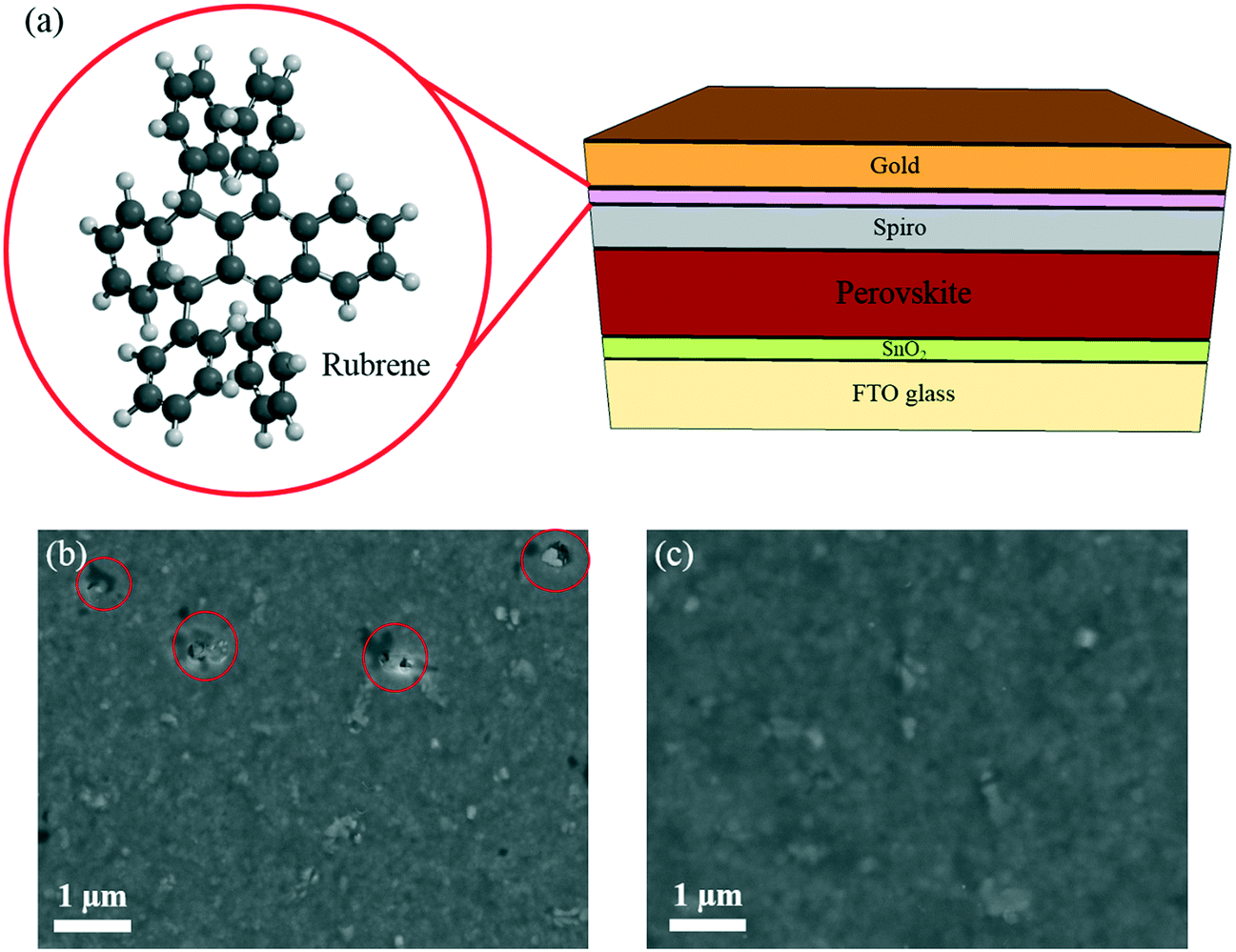 | ||
| Fig. 1 (a) Schematic of the device architecture used and the molecular structure of rubrene (white and grey spheres are hydrogen and carbon atoms, respectively). Top-view SEM images of (b) a spiro coated perovskite film and of (c) a rubrene coated spiro HTL. | ||
In order to study the role of rubrene, we have fabricated solar cells with only rubrene as the HTL. Fig. 2a shows the short current–voltage (J–V) curve of the PSC device based on rubrene as a HTL. This resulted in a short circuit current density (Jsc) of 19.1 mA cm−2, an open circuit voltage (Voc) of 0.92 V, a FF of 67%, and a PCE of 11.8% (reverse scan). We note that the device shows a slightly lower FF and PCE under forward scan. This result is significantly below the state-of-the art results showing that rubrene itself cannot act as an HTL. Following this observation, we evaporated rubrene on top of spiro as a modification layer and optimized the thickness of this interface layer, as shown in Fig. 2b. We observe an increase in values of FF and Voc for devices containing 5 and 10 nm thick rubrene layers. For thicker layers, this trend does not hold, and the performance parameters drop with lowered FF and Voc values due to poorer hole transporting properties and higher recombination rates. This demonstrates that the thickness of rubrene has an effective impact on the FF of the PSC device. We found that the optimum thickness of rubrene is around 5 nm.
 | ||
| Fig. 2 (a) J–V curve of the PSC device based on pure rubrene as a HTL (no spiro). (b) J–V curves of the PSC devices based on a spiro HTL with different thicknesses of the rubrene layer. Note that the devices were measured at a scan rate of 10 mVs−1. | ||
Fig. 3a shows a cross-sectional SEM image of the PSC device based on a spiro/rubrene HTL. After modification of the HTL by rubrene, the photovoltaic parameters of PSCs are improved in comparison to reference devices. Fig. 3b depicts the J–V curve characteristics of the best performing devices with and without a rubrene interface layer in the forward and reverse scan directions. Table 1 shows the collected photovoltaic parameters for the corresponding devices. The spiro based device (reference) gave a Jsc of 22.6 mA cm−2, a Voc of 1.105 V, a FF of 72%, and a PCE of 17.98% measured under reverse scan. In contrast, the device with a spiro/rubrene HTL exhibits a significant improvement of 7% for the FF with a Jsc of 22.4 mA cm−2, a Voc of 1.123 V, a FF of 79%, and a PCE of 19.87%. In particular, the spiro/rubrene device shows negligible hysteresis. The hysteresis index of the spiro and spiro/rubrene based devices are 2.33% and 1.12%, respectively (hysteresis index = ((PCEbackward − PCEforward)/PCEforward) × 100); see Table 1 for all the performance parameters. Fig. S4† demonstrates the photoluminescence spectra of the perovskite film deposited on glass with spiro and spiro/rubrene HTLs. As can be seen, the spiro/rubrene film shows a stronger quenching effect as compared to the spiro based film. This indicates that by adding rubrene, the device shows better carrier extraction and charge balance in the device, resulting in lower hysteresis.
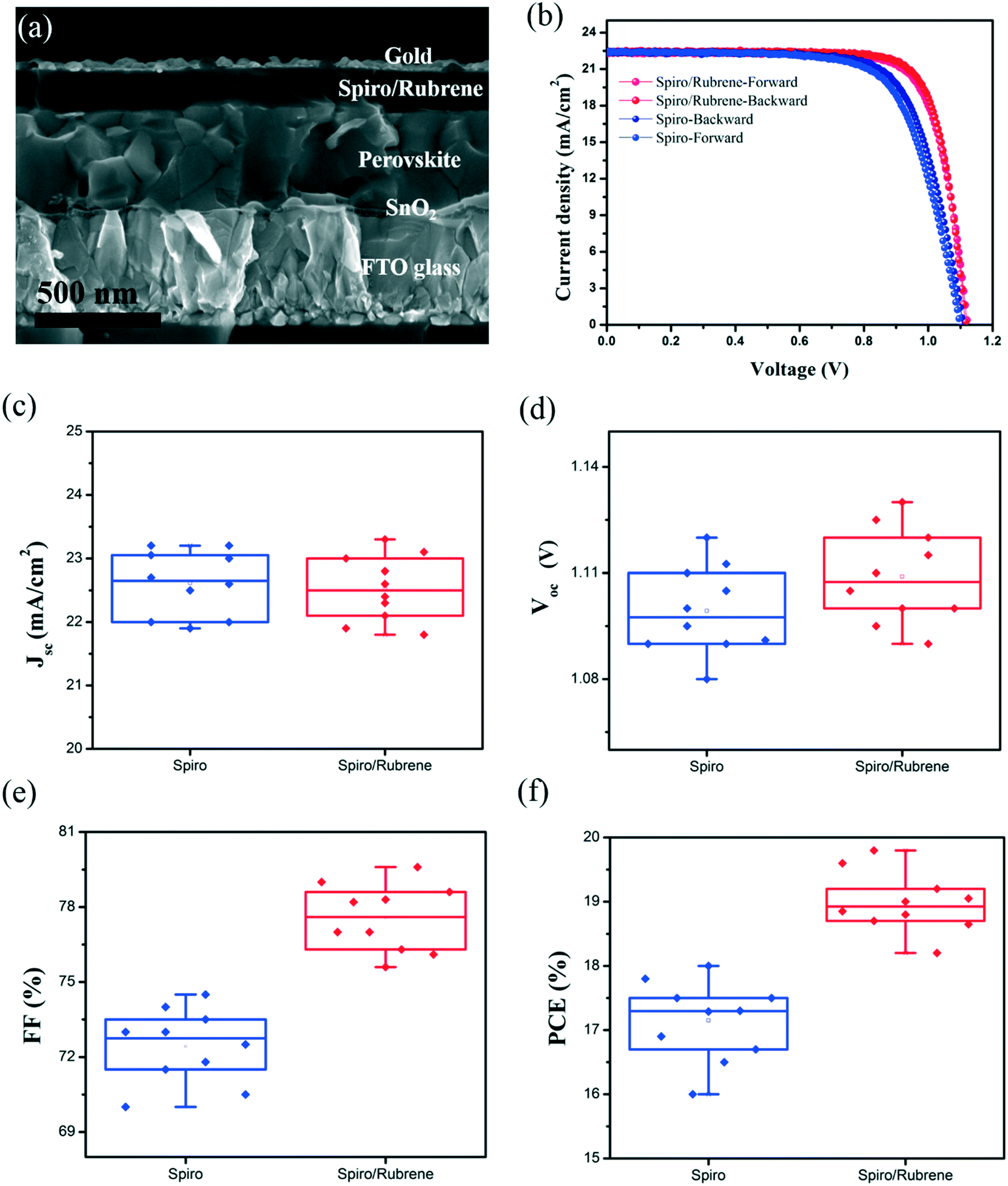 | ||
| Fig. 3 (a) Cross-sectional SEM image of the PSC device based on a rubrene/spiro HTL. (b) J–V curves of the best performing PSC devices based on pure spiro and rubrene/spiro HTLs in the forward and backward scan directions. (c–f) Distribution of photovoltaic parameters of PSC devices based on spiro and rubrene/spiro HTLs. | ||
| Sample | V oc (V) | J sc (mA cm−2) | FF (%) | PCE (%) | Hysteresis index (%) |
|---|---|---|---|---|---|
| Spiro-forward | 1.1 | 22.5 | 71 | 17.57 | 2.33 |
| Spiro-backward | 1.105 | 22.6 | 72 | 17.98 | |
| Spiro/rubrene-forward | 1.12 | 22.5 | 78 | 19.65 | 1.12 |
| Spiro/rubrene-backward | 1.123 | 22.4 | 79 | 19.87 |
Fig. 3c–f show the statistical histograms of photovoltaic parameters for 10 PSC devices with and without a rubrene interface layer. The average values of FF and Voc improved by 4.5% and 0.01 V, while the average value of Jsc decreased slightly.
Stability measurement of devices under light, heat, and humidity is still a big challenge for PSC devices.31–33 To study the stability of devices, the contact angle (CA) of water droplets on spiro and spiro/rubrene HTLs was measured, as shown in Fig. 4a and b. The CA of water droplets for spiro and spiro/rubrene layers was 38° and 62°, respectively. This shows that rubrene improves the stability of devices in a humid environment due to lower water wettability.
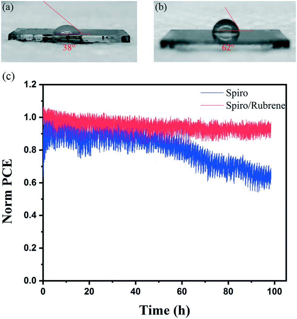 | ||
| Fig. 4 Contact angle measurement of a water droplet on (a) spiro and (b) spiro/rubrene HTLs. (c) Stability test of spiro and spiro/rubrene devices for 100 h under continuous full sun illumination and maximum power point tracking. | ||
In addition to increased stability against water ingress, the rubrene layer can cover the pinholes of the spiro HTL, which can stop detrimental gold migration (as shown in Fig. 1b and c). To further investigate this effect, the device stability was studied under constant illumination. Fig. 4c depicts the stability results for rubrene/spiro and spiro based devices at room temperature under a nitrogen atmosphere and under continuous light illumination and maximum power point tracking. Importantly, while the device with rubrene exhibits a slight decay after 100 h of continuous operation, the reference device has a 35% loss in PCE. This suggests that the spiro layer is a poor barrier against gold migration, consistent with the large number of observed pinholes within the entire layer, as shown in Fig. 1b.
Conclusions
In this work, we have modified the surface of a spiro HTL by applying a thin layer of rubrene. The additional interface layer improved mainly the FF of the planar PSC device covering pinholes within the bare spiro layer. The optimized device shows a high PCE of 19.87% with negligible hysteresis. Intriguingly, this device demonstrates great operational stability under continuous light illumination at maximum power point tracking.Materials and methods
Device fabrication
Nippon Sheet glass (10 Ω sq−1) was etched and patterned with zinc powder and diluted HCl solution. Then, the FTO glasses were washed with Triton X100 (1 vol% in deionized water), DI water, acetone, and ethanol by sonication followed by 15 min of UV ozone cleaning. Then, a solution of SnO2 nanocrystals (US Research Nanomaterials, 18 nm) was spin coated on substrates at 3000 rpm for 30 s, followed by annealing at 150 °C for 30 min. Before perovskite deposition, the substrates were exposed to UV ozone for 20 min. For the perovskite layer, MAPbI3 perovskite was deposited by spin coating a solution of PbI2 (1.2 M, TCI) and methylammonium iodide (1.15 M, dyesol) in a mixed solvent of DMF![[thin space (1/6-em)]](https://www.rsc.org/images/entities/char_2009.gif) :DMSO (4:1) at 1000 rpm for 10 s and 6000 rpm for 30 s. During the second step, 200 μL of an anti-solvent, i.e., chlorobenzene (CB), was dropped onto the film 10 seconds before the end of spinning. The perovskite film was annealed at 100 °C for 50 min. After annealing, a solution of spiro (52 mg/500 μL CB) containing 23 μL of 4-tert-butyl pyridine (TBP) and 12.34 μL of bis(trifluoromethylsulfonyl)imide lithium salt (Li-TFSI, Sigma-Aldrich) solution (520 mg/1 mL acetonitrile) was spin-coated at 4000 rpm for 20 s (at a ramp rate of 2000 s−1). Finally, gold was thermally evaporated as an electrode with a thickness of 100 nm.
:DMSO (4:1) at 1000 rpm for 10 s and 6000 rpm for 30 s. During the second step, 200 μL of an anti-solvent, i.e., chlorobenzene (CB), was dropped onto the film 10 seconds before the end of spinning. The perovskite film was annealed at 100 °C for 50 min. After annealing, a solution of spiro (52 mg/500 μL CB) containing 23 μL of 4-tert-butyl pyridine (TBP) and 12.34 μL of bis(trifluoromethylsulfonyl)imide lithium salt (Li-TFSI, Sigma-Aldrich) solution (520 mg/1 mL acetonitrile) was spin-coated at 4000 rpm for 20 s (at a ramp rate of 2000 s−1). Finally, gold was thermally evaporated as an electrode with a thickness of 100 nm.
Film characterization
The morphology of the perovskite, HTL, and device structure was studied by scanning electron microscopy (SEM, ZEISS Merlin). A Varian Cary 5 was used for UV-vis measurement. The steady-state photoluminescence (PL) was measured using a Fluorolog 322 (Horiba Jobin Yvon Ltd).Device measurement
A 450 W xenon lamp (Oriel, USA) as a light source and a digital source meter (Keithley model 2400, USA) were employed for the solar cell measurement. For the device measurement, a black aperture was applied on the device to obtain a fixed area of 0.16 cm2. All measurements were performed at a scan rate of 10 mVs−1. The light intensity was fixed to 1000 W m−2 for the device measurement. The range of voltage was between 0 and 1.2 V, with a step increment of 0.005 V. The delay time was 200 ms at each point.Stability test
The stability of the devices was studied using a Biologic MPG2 potentiostat under full AM 1.5. A sun-equivalent white LED lamp was used to measure the device stability. In this measurement, the maximum power point (MPP) of the devices was recorded every 10 seconds in a nitrogen environment under continuous light illumination. The substrate temperature was fixed to 25 °C using a Peltier element in direct contact with the devices. The active device area was fixed to 0.16 cm2. In this test, the J–V curves were measured every 15 min.Conflicts of interest
The authors declare no conflicts of interest for this work.Acknowledgements
M. M. T wants to thank the Laboratory of Photonics and Interfaces (LPI) at Ecole Polytechnique Fédérale de Lausanne (EPFL) and the School of Engineering at the Hong Kong University of Science and Technology for their support.References
- M. Saliba, T. Matsui, K. Domanski, J. Y. Seo, A. Ummadisingu, S. M. Zakeeruddin, J. P. Correa-Baena, W. R. Tress, A. Abate, A. Hagfeldt and M. Grätzel, Science, 2016, 354, 206–209 CrossRef PubMed.
- M. Saliba, J. P. Correa-Baena, M. Grätzel, A. Hagfeldt and A. Abate, Angew. Chem., Int. Ed., 2018, 57, 2554–2569 CrossRef PubMed.
- J. P. Correa-Baena, M. Saliba, T. Buonassisi, M. Grätzel, A. Abate, W. Tress and A. Hagfeldt, Science, 2017, 358, 739–744 CrossRef PubMed.
- M. M. Tavakoli, A. Simchi, X. Mo and Z. Fan, Mater. Chem. Front., 2017, 1, 1520–1525 RSC.
- M. Yavari, M. Mazloum-Ardakani, S. Gholipour, M. M. Tavakoli, S. H. Turren-Cruz, N. Taghavinia, M. Grätzel, A. Hagfeldt and M. Saliba, Adv. Energy Mater., 2018, 1800177 CrossRef.
- M. M. Tavakoli, K. H. Tsui, Q. Zhang, J. He, Y. Yao, D. Li and Z. Fan, ACS Nano, 2015, 9, 10287–10295 CrossRef PubMed.
- https://www.nrel.gov/pv/assets/images/efficiency-chart.png .
- Z. Wang, Q. Lin, F. P. Chmiel, N. Sakai, L. M. Herz and H. J. Snaith, Nat. Energy, 2017, 2, 17135 CrossRef.
- M. M. Tavakoli, L. Gu, Y. Gao, C. Reckmeier, J. He, A. L. Rogach, Y. Yao and Z. Fan, Sci. Rep., 2015, 5, 14083 CrossRef PubMed.
- S. Gholipour, A. M. Ali, J. P. Correa-Baena, S. H. Turren-Cruz, F. Tajabadi, W. Tress, N. Taghavinia, M. Grätzel, A. Abate, F. De Angelis and C. A. Gaggioli, Adv. Mater., 2017, 29, 1702005 CrossRef PubMed.
- M. M. Tavakoli, S. M. Zakeeruddin, M. Grätzel and Z. Fan, Adv. Mater., 2018, 30, 1705998 CrossRef PubMed.
- M. Zhang, J. S. Yun, Q. Ma, J. Zheng, C. F. J. Lau, X. Deng, J. Kim, D. Kim, J. Seidel, M. A. Green and S. Huang, ACS Energy Lett., 2017, 2, 438–444 CrossRef.
- M. M. Tavakoli, R. Tavakoli, Z. Nourbakhsh, A. Waleed, U. S. Virk and Z. Fan, Adv. Mater. Interfaces, 2016, 3, 1500790 CrossRef.
- J. Min, Z. G. Zhang, Y. Hou, C. O. Ramirez Quiroz, T. Przybilla, C. Bronnbauer, F. Guo, K. Forberich, H. Azimi, T. Ameri and E. Spiecker, Chem. Mater., 2014, 27, 227–234 CrossRef.
- M. M. Tavakoli, R. Tavakoli, S. Hasanzadeh and M. H. Mirfasih, J. Phys. Chem. C, 2016, 120, 19531–19536 CrossRef.
- M. Xu, J. Feng, X. L. Ou, Z. Y. Zhang, Y. F. Zhang, H. Y. Wang and H. B. Sun, IEEE Photonics J., 2016, 8, 1–7 Search PubMed.
- M. M. Tavakoli, F. Giordano, S. M. Zakeeruddin and M. Grätzel, Nano Lett., 2018, 18, 2428–2434 CrossRef PubMed.
- M. M. Tavakoli, P. Yadav, R. Tavakoli and J. Kong, Adv. Energy Mater., 2018, 1800794 CrossRef.
- T. Li, Y. Pan, Z. Wang, Y. Xia, Y. Chen and W. Huang, J. Mater. Chem. A, 2017, 5, 12602–12652 RSC.
- J. A. Christians, P. Schulz, J. S. Tinkham, T. H. Schloemer, S. P. Harvey, B. J. T. de Villers, A. Sellinger, J. J. Berry and J. M. Luther, Nat. Energy, 2018, 3, 68 CrossRef.
- M. Saliba, S. Orlandi, T. Matsui, S. Aghazada, M. Cavazzini, J. P. Correa-Baena, P. Gao, R. Scopelliti, E. Mosconi, K. H. Dahmen and F. De Angelis, Nat. Energy, 2016, 1, 15017 CrossRef.
- T. Matsui, I. Petrikyte, T. Malinauskas, K. Domanski, M. Daskeviciene, M. Steponaitis, P. Gratia, W. Tress, J. P. Correa-Baena, A. Abate and A. Hagfeldt, ChemSusChem, 2016, 9, 2567–2571 CrossRef PubMed.
- M. M. Tavakoli, D. Bi, L. Pan, A. Hagfeldt, S. M. Zakeeruddin and M. Grätzel, Adv. Energy Mater., 2018, 1800275 CrossRef.
- N. Arora, M. I. Dar, A. Hinderhofer, N. Pellet, F. Schreiber, S. M. Zakeeruddin and M. Grätzel, Science, 2017 DOI:10.1126/science.aam5655.
- Y. Hou, X. Du, S. Scheiner, D. P. McMeekin, Z. Wang, N. Li, M. S. Killian, H. Chen, M. Richter, I. Levchuk, N. Schrenker, Y. Hou, X. Du, S. Scheiner, D. P. McMeekin, Z. Wang, N. Li, M. S. Killian, H. Chen, M. Richter, I. Levchuk, N. Schrenker, E. Spiecker, T. Stubhan, N. A. Luechinger, A. Hirsch, P. Schmuki, H.-P. Steinrück, R. H. Fink, M. Halik, H. J. Snaith and C. J. Brabec, Science, 2017, 358, 1192–1197 CrossRef PubMed.
- S. Gholipour, J. P. Correa-Baena, K. Domanski, T. Matsui, L. Steier, F. Giordano, F. Tajabadi, W. Tress, M. Saliba, A. Abate and A. Morteza Ali, Adv. Energy Mater., 2016, 6, 1601116 CrossRef.
- X. Zheng, B. Chen, J. Dai, Y. Fang, Y. Bai, Y. Lin, H. Wei, X. C. Zeng and J. Huang, Nat. Energy, 2017, 2, 102 Search PubMed.
- M. C. Jung, S. R. Raga, L. K. Ono and Y. Qi, Sci. Rep., 2015, 5, 9863 CrossRef PubMed.
- G. Ji, G. Zheng, B. Zhao, F. Song, X. Zhang, K. Shen, Y. Yang, Y. Xiong, X. Gao, L. Cao and D. C. Qi, Phys. Chem. Chem. Phys., 2017, 19, 6546–6553 RSC.
- N. J. Jeon, J. H. Noh, Y. C. Kim, W. S. Yang, S. Ryu and S. I. Seok, Nat. Mater., 2014, 13, 897 CrossRef PubMed.
- R. B. Dunbar, B. C. Duck, T. Moriarty, K. F. Anderson, N. W. Duffy, C. J. Fell, J. Kim, A. Ho-Baillie, D. Vak, Y. Wu and K. Weber, J. Mater. Chem. A, 2017, 5, 22542–22558 RSC.
- R. Roesch, T. Faber, E. von Hauff, T. M. Brown, M. Lira-Cantu and H. Hoppe, Adv. Energy Mater., 2015, 5, 1501407 CrossRef.
- M. Saliba, Science, 2018, 359, 388–389 CrossRef PubMed.
Footnote |
| † Electronic supplementary information (ESI) available. See DOI: 10.1039/c8me00036k |
| This journal is © The Royal Society of Chemistry 2018 |