 Open Access Article
 This Open Access Article is licensed under a Creative Commons Attribution-Non Commercial 3.0 Unported Licence
The ultimate switching speed limit of redox-based resistive switching devices
Stephan
Menzel
 *a,
Moritz
von Witzleben
b,
Viktor
Havel
b and
Ulrich
Böttger
b
*a,
Moritz
von Witzleben
b,
Viktor
Havel
b and
Ulrich
Böttger
b
aForschungszentrum Jülich, Peter Grünberg Institut (PGI-7), 52425 Jülich, Germany. E-mail: st.menzel@fz-juelich.de
bRWTH Aachen University, Institut für Werkstoffe der Elektrotechnik (IWE 2), 52074 Aachen, Germany
First published on 24th August 2018
Abstract
In contrast to classical charge-based memories, the binary information in redox-based resistive switching devices is decoded by a change of the atomic configuration rather than changing the amount of stored electrons. This offers in principle a higher scaling potential as ions are not prone to tunneling and the information is not lost by tunneling. The switching speed, however, is potentially smaller since the ionic mass is much higher than the electron mass. In this work, the ultimate switching speed limit of redox-based resistive switching devices is discussed. Based on a theoretical analysis of the underlying physical processes, it is derived that the switching speed is limited by the phonon frequency. This limit is identical when considering the acceleration of the underlying processes by local Joule heating or by high electric fields. Electro-thermal simulations show that a small filamentary volume can be heated up in picoseconds. Likewise, the characteristic charging time of a nanocrossbar device can be even below ps. In principle, temperature and voltage can be brought fast enough to the device to reach the ultimate switching limit. In addition, the experimental route and the challenges towards reaching the ultimate switching speed limit are discussed. So far, the experimental switching speed is limited by the measurement setup.
Introduction
Redox-based resistive switching devices have attracted great attention due to their potential use in future non-volatile memories, logic-in-memory or neuromorphic applications.1 Based on their switching mechanism, it can be distinguished between devices showing a thermo-chemical mechanism (TCM), electrochemical metallization (ECM), and a valence change mechanism (VCM).2 In contrast to classical DRAMs, SRAMs or flash memories, the binary information in resistive switching devices is decoded by a change of an atomic configuration rather than changing the amount of stored electrons. The change of the atomic configuration is achieved by the movement of ionic defects. Memories based on the storage of electrons in a potential well suffer from two different drawbacks. The electrons can leave the potential well if they have sufficient thermal energy to escape over the potential barrier. In addition, electrons can tunnel through the potential barrier if it is thin enough. This latter loss mechanism is not present in memories exploiting atomic configurations due to the high atomic mass. Thus, redox-based resistive switching devices have a higher scaling potential as electronic memories.3,4 In contrast, the switching speed is potentially smaller as the ionic mass is much higher than the electron mass. Still, it is not clear how fast a redox-based resistive switching device can switch.Resistive switching in the low nanosecond regime has been frequently demonstrated.5–13 Studies showing switching in the sub-nanosecond regime, however, are rare. In 2011, Torrezan et al. demonstrated that the set and reset switching of Ta2O5-based VCM devices is faster than 120 ps.14 Other groups observed set and reset switching times below 500 ps.15–17 Switching below 100 ps was shown for a Pt/SiO2-based device18 and the record switching speed of <85 ps was achieved for a nitride-based resistive switch.19 In all of these studies, however, it was concluded that the switching speed was still limited by the measurement setup.
In this work, the ultimate switching speed limit of redox-based resistive switching devices is discussed. First, a theoretical limit based on the underlying atomic processes under high electric field and temperature will be derived. It will be further discussed to what extent the theoretical limit is influenced by the speed of Joule heating and the speed of charging the device. Besides the theoretical discussion, an experimental route towards reaching the ultimate switching speed limit will be presented.
The theoretical limit
Analytical analysis
The ultimate switching speed limit is closely linked to the atomistic processes that cause the switching event in the metal/insulator/metal memory stack. These processes are the migration of ionic defects in the insulating material, redox processes occurring at the metal/insulator interfaces and the nucleation of new phases (or electro-crystallisation if the nucleation involves a charge-transfer process) within the insulating material, as discussed in ref. 20. For example, it has been demonstrated that the non-linearity of the switching kinetics in filamentary switching VCM cells originates from the temperature-accelerated drift of the ionic defects.21–26 In AgI-based ECM cells, the strong nonlinearity of the switching kinetics results from the nucleation of the conducting filament at the inert electrode at low voltages, the redox reactions at the metal/insulator interfaces at intermediate voltages and ion migration at very high voltages.27 Also for other ECM systems these processes have been identified as rate-limiting.28–34 In the case of a unipolar switching TiO2-based TCM cell, the formation of a filamentary-shaped Magnéli phase was observed by the means of TEM.35,36 This phase transition, however, is induced by the movement of the ionic defects within the switching layer. In the end, the slowest process involved in the switching will determine the switching speed. Which process is the slowest one, will depend on the voltage applied and on the ambient temperature.In order to derive the ultimate switching speed limit from theory, one needs to consider the mathematical rate equations for the three processes. The electro-crystallisation rate is given by
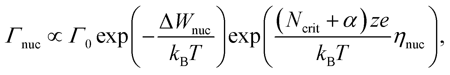 | (1) |
 | (2) |
In eqn (2), c is the concentration of the moving ionic defects, a is mean hopping distance, f is the attempt frequency, ΔWhop is the hopping barrier, and E is the electric field. The electron (charge)-transfer processes determining the speed of the redox processes at the metal/insulator interfaces can be described by the Butler–Volmer equation:
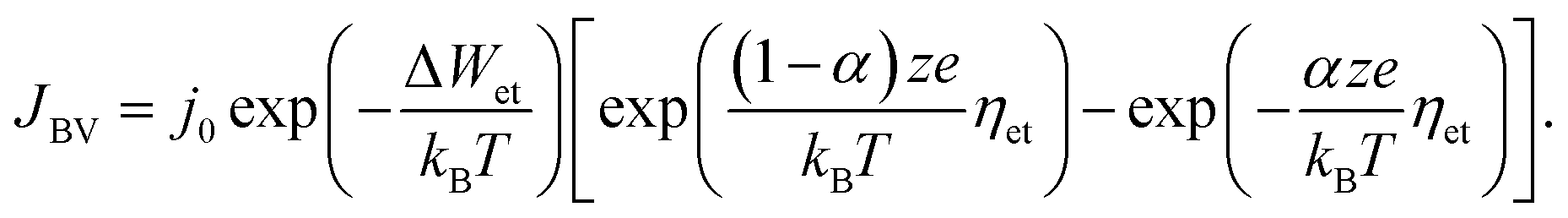 | (3) |
Eqn (1)–(3) exhibit a very similar form. All the processes obey an Arrhenius-type law and depend nonlinearly on the applied electric potential (electric field). For high electric fields the sinh term can be approximated with an exponential function, which results in the more generalized relation for the process rate
 | (4) |
In the following, we will assume that the ion hopping process will determine the ultimate switching speed. As all processes have the same functional form, this assumption does not lead to a loss of generality. From a physical perspective this is a very likely scenario as the ionic defects need to travel some distance (so many hops are involved), but the other processes only involve a single transition at an interface.
Using eqn (2), the relation Jhop = cev as well as assuming high electric fields, the drift velocity v results in
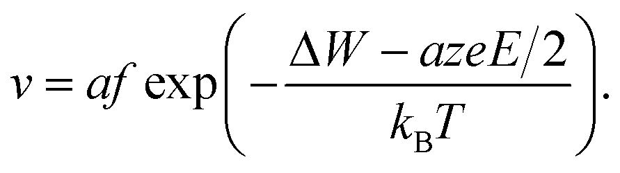 | (5) |
It is clear that the drift velocity will get maximal if the temperature goes to infinity, that is,
 | (6) |
With respect to the electric field, the drift velocity will be maximized if the activation energy ΔW is lowered as much as possible by the electric field. From a physical point of view, a barrier lower than zero is not possible. In fact, the formulation in eqn (5) is incorrect for very high electric fields as has been discussed by Genreith-Schriever et al.37 The authors considered a sinusoidal potential landscape where the minima give the stable sites for the hopping ionic defects. By application of an external field E the energy landscape eψ(x) is tilted according to
eψ(x) = ΔWhop![[thin space (1/6-em)]](https://www.rsc.org/images/entities/char_2009.gif) sin(2πx/a) − eEx. sin(2πx/a) − eEx. | (7) |
The effective hopping barrier can be simply derived from evaluating the potential difference between a local minima and its neighbouring local maximum. Plotting the energy landscapes for different electric fields clearly shows that the barrier in the direction of the electric field is lowered, whereas it is increased in the reverse direction (see Fig. 1a). For very high electric fields the maxima and minima vanish and eventually the energy landscape approaches eψ(x) = −eEx. Thus, at very high electric fields the acceleration would not become exponential anymore. Fig. 1b shows the difference from calculating the effective hopping barrier as in eqn (5) or by extracting it from the energy landscape in Fig. 1a. The standard approach according to eqn (5) clearly overestimates the barrier lowering for high electric fields and would even predict negative hopping barriers at very high electric fields. Such a negative barrier will appear at even lower electric fields if a field-acceleration factor is used as proposed in ref. 38. First of all, this field-enhancement factor is not consistent with the derivation of the ionic hopping process based on the inner energy landscape.37,39–42 The more severe issue is that the exponential law is maintained even for negative barriers, which lead to drift velocities higher than the speed of light at moderate applied fields, e.g. for the parameters used in ref. 43 and 44. This issue is illustrated in Fig. 1c, which shows the drift velocity calculated according to eqn (5) (red solid line) and using the effective hopping barrier extracted from the energy landscape (blue solid line). In the negative barrier regime the calculated drift velocity exceeds the speed of light, i.e. c0 ≈ 3 × 10⁸ m s−1. The difference between the two approaches appears at electric fields relevant for scaled redox-based resistive switching memories: typically, a few volts are applied to a few nanometre thick active switching layers. If Joule heating is considered, the difference between the two approaches becomes less dramatic. In this case, the increase in drift velocity is dominated by Joule heating (dashed lines). In addition, the quotient in the exponential function becomes smaller for increasing temperature, which leads to a saturation of the drift velocity at high electric fields.
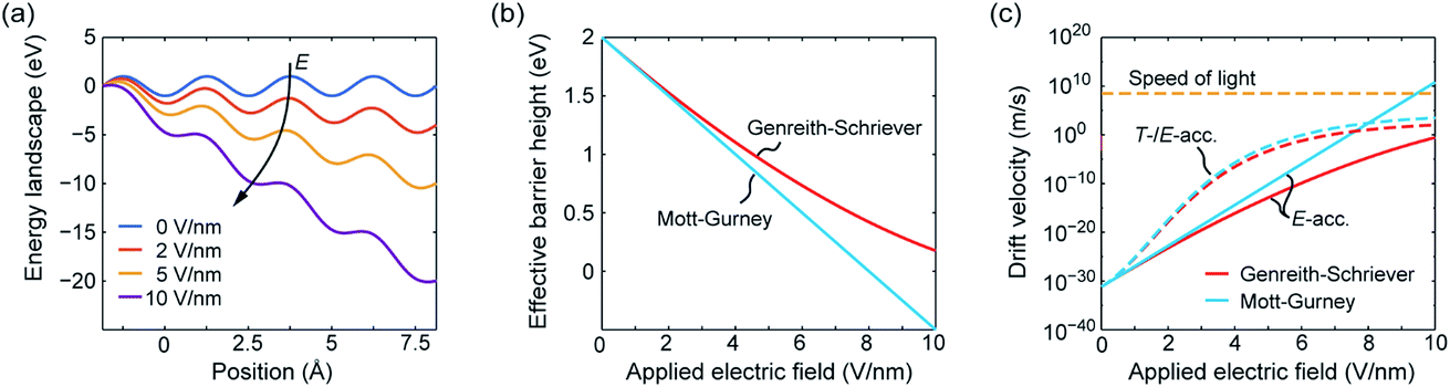 | ||
| Fig. 1 (a) Energy landscape calculated using eqn (7) for different applied electric fields. The effective barrier height and the corresponding drift velocity calculated according to Mott–Gurney (blue lines) and Genreith-Schriever (red lines) are shown in (b) and (c), respectively. In (c) the drift velocity is illustrated for assuming only electric field acceleration at T0 = 300 K (solid lines) and for including additional Joule heating effects (dashed lines). The temperatures resulting from Joule heating are calculated using T = T0 + RthV2/R assuming an ohmic resistance. The parameters used are a = 0.25 nm, ΔWhop = 2 eV, z = 2, f = 1 THz, R = 100 kΩ, and Rth = 1.6 MW K−1. The electric field is supposed to drop over 1 nm. | ||
In ref. 37 it was further demonstrated that the ionic crystal becomes unstable at such high electric fields and all constituting ions start to move. It should be noted that this result is independent of the form of the interatomic energy landscape as the amplitude will be always given by eΔWhop. The consideration of the potential landscape under high electric fields underpins the assumption that the minimum possible effective migration barrier is zero. Hence, the maximum drift velocity under the limit of high electric fields is given by
 | (8) |
To conclude, independent of the means of process acceleration, the theoretical analysis yields the same maximum drift velocity. Finally, the ultimate switching speed is given by the phonon frequency. For typical values of f ≈ 1–10 THz and considering that a single event is sufficient to result in a resistance change, a lower limit of the switching time of about a picosecond is expected.
To reach this limit, however, the temperature and/or the electric field are supposed to be applied with the same speed. In the following we will discuss if this condition can be fulfilled.
Joule heating speed limit
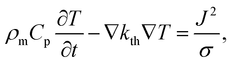
The speed of Joule heating is assessed by means of transient electro-thermal simulations using a 3D model of a filamentary switching VCM (or TCM) cell. For ECM cells the currents at which the set transition triggers are typically too small to cause any Joule heating effects. In addition, the materials forming the filament in ECM cells (typically Ag or Cu) are excellent heat conductors and less Joule heating is expected. In contrast, the oxide materials of VCM and TCM are bad thermal conductors with thermal conductivities around 1 W m−1 K−1.The geometry of the ReRAM cell, which resembles a typical lab-scale device, is shown in Fig. 2a. It consists of a 100 nm thick Si 1 μm2 substrate layer, followed by a 100 nm thick SiO2 layer and a crossbar structure on top. The top and bottom electrodes are 10 nm thick and 50 nm wide resulting in a junction of 50 × 50 nm2. The two electrodes are separated by a 5 nm-thick switching layer, which is a quite reasonable thickness of a state-of-the-art device. In the middle of the junction a cylindrical filament with a diameter of 10 nm is assumed. This value is in agreement with different spectro-microscopic observations of filaments in resistive switching devices.24,35,45,46 To calculate the temperature distribution in this structure, the transient heat equation,
 | (9) |
| −∇J = ∇σ∇φ = 0, | (10) |
| σ = σ0/(1 + αth(T − T0)). | (11) |
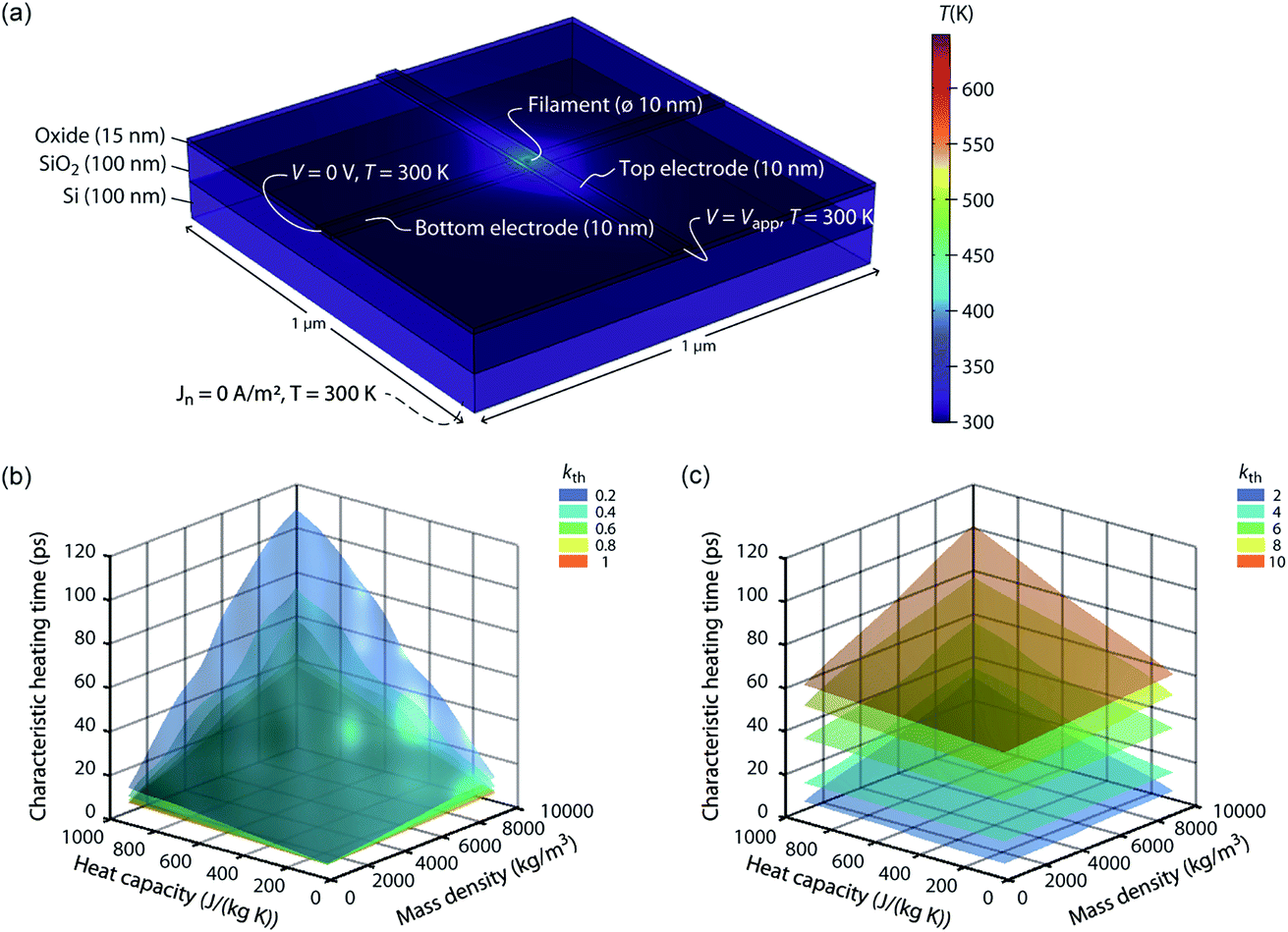 | ||
| Fig. 2 (a) Simulation geometry and boundary conditions for solving eqn (9) and (10). The active oxide switching region at the junction of the two electrodes has only a thickness of 5 nm. The bottom electrode is embedded in the oxide layer covering the whole substrate. The dashed line indicates the boundary conditions at the bottom of the Si substrate. For all boundaries not labelled, Neumann boundary conditions were chosen, i.e., the heat flux and the normal current flow are set to zero. A typical temperature distribution is shown in colour. The oxide material parameters for this simulation are kth = 1 W m−1 K−1, Cp = 500 J kg−1 K−1, and ρm = 5000 kg m−3. The simulated characteristic heating times are shown as a function of the heat capacity and the mass density for different thermal conductivities, i.e., in (b) kth = {0.2, 0.4, 0.6, 0.8, 1} W m−1 K−1 and in (c) kth = {2, 4, 6, 8, 10} W m−1 K−1. | ||
In eqn (11)σ0 is the electric conductivity at the reference temperature T0 and αth is the first order temperature coefficient. The thermal conductivity of the metal electrodes is connected to the electronic conductivity via the Wiedemann–Franz law
| kth = σLT, | (12) |
000 kg m−3, Cp varies from 100 J kg−1 K−1 to 1000 J kg−1 K−1, and the thermal conductivity kth is varied from 0.1 W m−1 K−1 to 10 W m−1 K−1. The remaining simulation parameters are listed in Table 1. Apart from the filament region, the material parameters are identical to the ones determined in a previous publication.22
| Pt (top electrode) | Ti (bottom electrode) | Oxide | SiO2 | Si | |
|---|---|---|---|---|---|
| Electric conductivity σ | 4.76 × 10⁶ S m−1 | 1.26 × 10⁶ S m−1 | 1 × 10³ S m−1 (filament) | 1 × 10⁻¹⁶ S m−1 | 1 × 10⁻⁶ S m−1 |
| 1 × 10⁻¹⁰ S m−1 (matrix) | |||||
| Thermal conductivity kth | Eqn (12) | Eqn (12) | Variable | 1.2 W m−1 K−1 | 4 W m−1 K−1 |
| Heat capacity Cp | 133 J kg−1 K−1 | 522 J kg−1 K−1 | Variable | 1000 J kg−1 K−1 | 100 J kg−1 K−1 |
| Mass density ρm | 21450 kg m−3 |
4506 kg m−3 | Variable | 2196 kg m−3 | 1000 kg m−3 |
| Temperature coefficient αth | 1.39 × 10⁻³ K−1 | 1.13 × 10⁻³ K−1 | — | — | — |
From the simulation results we extracted the time evolution of the maximum temperature in the filament during the applied pulse. Based on this data we determined the characteristic heating time constant τth that is required to achieve 63% of the static maximum temperature. The final maximum temperature during the transient simulation at t = 50 ns deviates less than 0.25% from the static one, which was determined by an additional static electro-thermal simulation at 2 V. In Fig. 2b and c the characteristic heating time is plotted as a function of the variable parameters Cp, ρm, and kth. Each coloured surface represents the results for the thermal conductivity specified in the figure legends. Two trends can be observed: The thermal time constant increases more or less linearly with the increase of the heat capacity of the oxide material and for increasing mass densities. This result is consistent with the theory of heat conduction, which predicts a linear relation τth ∝ Cpρm.47 The dependence between the thermal time constant and the thermal conductivity is a lot more complicated. The relation of the thermal conductivity of the oxide material and the surrounding materials will influence the heated volume, which is another crucial factor for determining the thermal time constant.47 In our case it seems that the thermal time constant decreases up to a thermal conductivity of 1 W m−1 K−1 and then increases again. How strong this effect is, however, depends also on the value of the two other parameters. Overall, the characteristic heating time stays well below 120 ps, which means heating will take place on the order of tens of picoseconds or even less. Of course, a sufficiently high temperature is required to accelerate the processes driving the resistive switching. The extra thermal time constant, however, is independent of the applied voltage. So, to achieve a high temperature, the applied voltage can be increased leading to higher temperatures during the heating phase. This is of most importance for oxides with a high thermal conductivity. In our simulations, the steady state temperature is lowest for these oxides.
Joule heating is based on the scattering of electrons at phonons. Only by these events can the electron and the phonon temperature be balanced. To reach the thermal equilibrium a couple of collisions between the energy carriers is required, which should result in an equilibration time of the order of the phonon frequency.48 Therefore, the ultimate switching speed limit and the limit of Joule heating are in the same range. Joule heating in the low picosecond range has been experimentally demonstrated in photoconductive switch electrodes.49 The latter result supports the claim of sufficiently fast Joule heating in order to reach the ultimate switching speed limit.
Charging speed limit
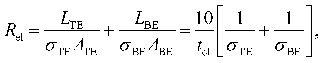
In the previous section an ideal voltage pulse with a rise time of 1 fs was assumed, but is it really possible to apply this voltage so fast to the cell when parasitic capacitances are taken into account? To answer this question the characteristic charging time is analysed. The same structure as in the previous section is assumed (see Fig. 3a). First, we consider only the charging time of the device itself including the resistance of the electrodes Rel, the resistance of the filament channel Rdev and the device capacitance Cdev. The corresponding equivalent circuit diagram is shown in the inset of Fig. 3a. For a scaled crossbar structure it is important to include parasitic capacitances in addition to the parallel plate capacitance C‖. Here, we consider the four parasitic angle capacitances C∠ as illustrated in Fig. 3b. As the dimensions of the electrodes are identical all four angle capacitances are identical. The overall device capacitance then reads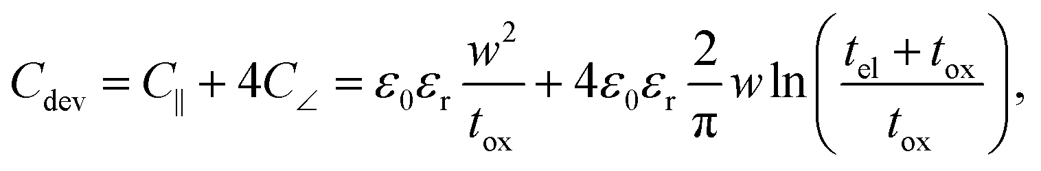 | (13) |
 | (14) |
| Rdev = tox/(σfilA) = tox/(σfilπr2). | (15) |
 | ||
| Fig. 3 (a) The assumed geometry of the ReRAM device (not to scale). It is similar to the one used in the previous section. The equivalent circuit is drawn in the inset. The cross-section along the Pt electrode is shown in (b). The parallel plate capacitance C‖ originates from the direct overlap of both electrodes. Here the field lines are straight. The additional curved field lines correspond to the parasitic angle capacitances C∠. The device capacitance and the characteristic time constant are plotted in (c) as a function of the line width for different dielectric constant of the oxide layer. | ||
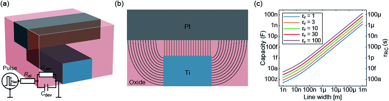
In eqn (13) it is assumed that the length of the top/bottom electrode (TE/BE) is ten times the width of the electrode. The values for the conductivities are given in Table 1 assuming T = 300 K.
By solving the differential equation describing the equivalent circuit diagram in Fig. 3a, a time-dependent expression for the device voltage results:
 | (16) |
The characteristic RC-time τ of this circuit is
 | (17) |
Under the assumption Rdev ≫ Rel, eqn (17) simplifies to τ = RelCdev. This means that the characteristic time constant is not limited by the filament resistance itself but rather by the electrode resistance in series.
Fig. 3c shows the calculated device capacitance and characteristic time constant in dependence of the line width w. As shown in eqn (14), Rel does not depend on w and therefore only Cdev depends on w. Consequently, τ and Cdev have the same dependence on w. As expected, larger dimensions lead to higher device capacitances and, therefore, to longer charging times. Both the device capacitance and the characteristic time constant depend linearly on the dielectric constant of the active material. This is also illustrated in Fig. 3c. For very small structures, theoretical charging times of less than 1 ps can be achieved.
Based on these analytical analyses we can draw the following conclusion. For a scaled crossbar device, the characteristic time constant is small enough to enable the reaching of the intrinsic switching speed limit. To this end, the voltage needs to be brought to the device without any delay due to the measurement setup. It is clear that any capacitance in parallel to the device capacitance or any inductance in series would lead to an increase of the characteristic time constant. An additional problem arises in the sub-nanosecond regime. In this regime, high frequency effects need to be taken into account due to the wavelength being comparable to the dimension of the physical circuits.
Experimental: approaching the limit
The determination of the lower limits of both the charging and Joule heating speed is beyond the possibility of current measurement equipment. Also the fast switching times predicted by the models of Mott–Gurney and Genreith-Schriever have not been reached yet. As mentioned in the introduction, it is possible so far to study switching times in the sub-nanosecond regime, which allows most of the relevant part of the set kinetics to be covered. This section aims to explain the measurement techniques required for such short timescales.Two specific experimental challenges have to be faced. Firstly, the applied pulses to the device need very short rise and fall times and must have a relatively high amplitude (>1 V), too. Commercial solutions that are able to generate such short pulses usually have amplitudes below 1 V and are only available as pattern generators with relatively high repetition rates. For probing the switching event, however, this is not favourable. Torrezan et al. solved this issue by an experimental setup that includes a commercial pattern generator, an additional amplifier and a switch that separates one pulse from the generated pattern.14 The fastest switching time of a ReRAM device has been measured with this setup and amounts to 85 ps.19 The second challenge is to design the experiment in a way that the generated signal is preserved until it reaches the ReRAM device. Therefore, every component in the setup has to be chosen carefully and requires a high bandwidth. To provide proper impedance matching at the contact between the sample and the high frequency probes, coplanar waveguides are usually used, in which the ReRAM device is embedded (see Fig. 4). It consists of two ground conductors and the middle signal conductor. Its characteristic impedance can be designed by the dimensions of the line width and the spacing. Usually it is set to 50 Ω as this is the characteristic impedance of all other components in the setup. To provide ideal signal preservation, this transmission line needs to be terminated by 50 Ω in order to minimize effects of parasitic capacitances and inductances. The resistance of a ReRAM device, however, is usually much higher and therefore those capacitive effects still have to be considered. To illustrate this measurement technique, an exemplary measurement is provided in the following.
 | ||
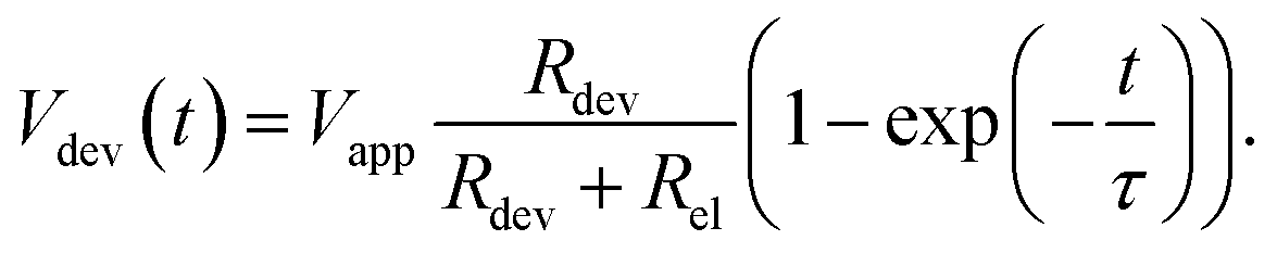
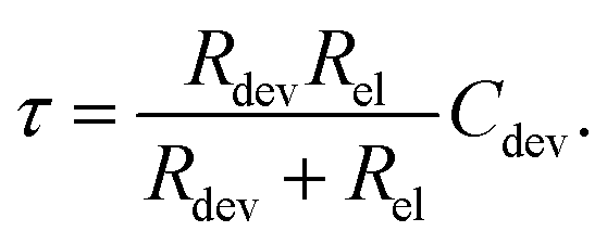
| Fig. 4 (a) An optical microscope picture of the coplanar waveguide structure. The inset is a zoom into the centre, where the ReRAM device is located. The dotted lines label the profiles A and B, which are shown in (b). The profile A is lengthwise to the sample and the profile B corresponds to its cross-section. The Si substrate has a high resistivity ρ > 10 Ω cm−1 and the top 450 nm are oxidized. The bottom electrode consists of a 5 nm-thick Ti adhesion layer and a 25 nm-thick Pt layer and has been deposited by means of DC-sputtering. The 5 nm-thick Ta2O5 layer is deposited via RF-sputtering. Both layers were structured using ion beam etching. The top electrode consists of 5 nm Ta and 25 nm Pt, which have been deposited by e-beam evaporation. It was structured by means of a lift-off process. | ||
The setup used in this paper is similar to the one presented by Torrezan et al.14 The device (Pt/Ta2O5/Ta) is embedded in a coplanar waveguide structure with a characteristic impedance of 50 Ω. The overlap of top and bottom electrodes amounts to 20 × 30 μm2. As explained above, this results in a significant capacitance of the ReRAM device and, therefore, in long charging times. An optical microscope picture of this structure is shown in Fig. 4a and the cross-sections perpendicular and along the middle electrode are depicted in Fig. 4b. Additional information about the manufacturing can be found in the figure caption.
An exemplary measurement result is shown in Fig. 5.17 Before the application of the pulse the device was programmed into the HRS of about 1 kΩ. Then, a short pulse with an amplitude of −10.8 V was applied and the current was measured with a real-time oscilloscope. The measured current is shown in Fig. 5a and consists in parts of a capacitive current and the current through the device. The full width at half maximum (FWHM) of the pulse is about 350 ps. Subsequently, an I–V sweep was carried out (see Fig. 5b). It started in a low resistive state and, thereby, proves that the ReRAM device was successfully set to the LRS during the application of the 350 ps pulse. If longer pulses with smaller amplitude are applied, resolving the switching event at a nanosecond time scale becomes possible. Fig. 5c shows an example of a 10 ns pulse with an amplitude of −1.8 V. After a significant capacitive current at the beginning of the pulse, the device switched to the LRS. In this example, the switching event occurred after about 5 ns and can be seen in a second current increase. A typical set event would be a quite abrupt switching event (at least if the current in the HRS is not too high). Here, the parasitic capacitances mask the intrinsic device behaviour. To extract more information from the current transients in the sub-nanosecond regime, the parasitic capacitances need to be lowered. In addition, the charging of the device limits the switching speed. In the experiment, the slow charging can be overcompensated by simply applying voltage pulses with higher magnitude than actually required. In the end, the maximum voltage that can be supplied by the pulse generator limits this approach and thus the switching speed.
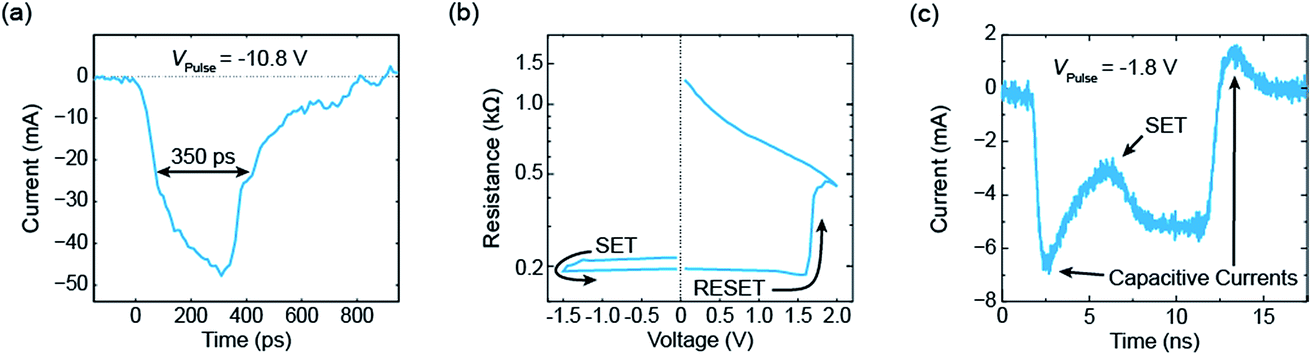 | ||
| Fig. 5 Selected measurements from ref. 17. (a) The current response of an electrical voltage pulse with an amplitude of −10.8 V. Its FWHM amounts to 350 ps. The subsequent I–V sweep is shown in (b). As it starts in the LRS, the ReRAM device must have set during the application of the 350 ps pulse. In (c) the current response of a 10 ns voltage pulse with an amplitude of −1.8 V is shown. It is possible to resolve the set event after about 5 ns. | ||
Discussion: designing fast redox-based resistive switching devices
Based on our theoretical analyses some design guidelines for developing fast redox-based resistive switching devices can be deduced. The challenge is to achieve very fast switching at reasonable operating voltages and at the same time a high read-disturb immunity. This challenge is also known as the voltage–time dilemma.2,21 Assuming without loss of generality the ionic drift velocity of eqn (5) as the limiting process, the switching time becomes | (18) |
The constant K will include the distance the ions have to travel (cf.ref. 21), but also the ion concentration c (cf.eqn (2)). The local temperature depends on the dissipated electrical power Pel and is approximated by
| T = T0 + RthPel = T0 + RthI(V)V. | (19) |
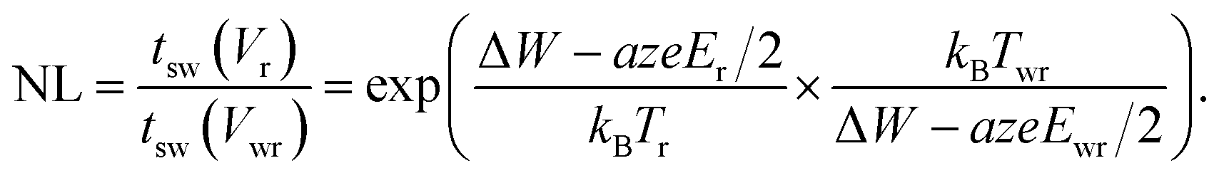
In eqn (19), T0 is the ambient temperature and Rth is the effective thermal resistance of the specific device configuration. It includes the heat dissipation via the electrodes and the oxide matrix as well as the geometry of the heated volume.50 Based on eqn (18) and (19), design rules for developing ultrafast ReRAMs can be deduced already. To evaluate the voltage–time dilemma, the figure of merit NL is introduced, according to
 | (20) |
This figure of merit describes the ratio between the switching time at a read voltage Vr and the switching time at the write voltage Vwr. It is straightforward to define likewise the local temperatures Tr and Twr and the active electric fields Er and Ewr at the read and write voltage, respectively.
First, let us consider a ReRAM device, the operation of which is only accelerated by the electric field without any Joule heating. This condition applies to ECM cells due to their low operation currents and to area-dependent switching VCM systems. In the latter case, the current density is too low to induce any significant Joule heating. ECM devices show a filamentary switching operation, but the switching currents are typically quite low and the electrode materials involved (Ag or Cu) are excellent heat conductors, effectively dissipating the heat.51 To achieve fast switching in these devices, the ionic mobility at room temperature should be as high as possible. Analysing eqn (18) gives two viable routes. The more obvious one is to reduce the thickness of the oxide layer. In this way, the ions have to move a shorter distance, thus reducing the constant K. Even more important is the fact that the electric field E will increase, which gives rise to an exponential decrease of the switching time. Another advantage of reducing the oxide thickness is the potential reduction of the switching energy, as lower voltages need to be applied to achieve the same switching speed. Higher electric fields can also be generated by fabrication. It is clear that the local electric field is enhanced at sharp edges.52 Deliberately introducing such sharply-edged structures will thus enable faster switching devices. The reduction of the oxide thickness is, however, limited. Below 2 nm significant electron tunnelling current from one electrode to the other should set in, which reduces the resistance ratio RHRS/RLRS. Further, increasing the electric field will also enhance the switching speed at read voltages. The figure of merit NL will stay more or less constant if the oxide thickness is reduced. So, there is a trade-off between fast switching speed and device retention.
The second option to accelerate the switching speed is to increase the ionic current density driving the switching process by increasing the ion concentration (compare the discussion of the switching kinetics of ECM devices in ref. 20). For ECM devices, it has been shown that the choice of the counter electrode material effectively influences the speed of the redox reactions at the active metal/insulator-interface, and thus the injected amount of the active ionic species.33,53,54 In addition, mechanical stress might influence the ionic mobility to some extent. Again, the increased ionic mobility will come with the expense of a faster switching at the read voltage. As the ionic mobility will influence mainly K, the figure of merit NL will keep constant. Again, there is a trade-off between fast switching speed and data retention. A way out of this dilemma would be if read and write operations are limited by different physical processes. Thus, the switching speed of read and write operations can be tuned separately. For different ECM devices it has been shown that the switching speed is determined by a nucleation reaction or electron-transfer reactions at lower voltage, but by the ionic drift at higher voltages.20,27,34 Redox reactions at the metal/oxide interfaces also play a role in VCM devices,55–57 but up to now it is not clear how they influence the switching speed in different voltage regimes.
For filamentary VCM systems, it was shown that local Joule heating will finally determine the switching speed at write voltages and is the origin of the nonlinear switching kinetics.20–22 Higher local temperatures will lead to faster switching speed. According to eqn (19), the value of the effective thermal resistance is the design parameter of choice. To increase this parameter, the device design should be optimized with respect to its thermal properties. First of all, an oxide with a low thermal conductivity could be chosen. This will increase the heating efficiency of the device and reduce the lateral heat loss via the oxide layer. In addition, a lateral heat barrier could be introduced. A material with a lower thermal conductivity than the switching oxide, surrounding the active switching volume in a kind of via structure, will lead to a lateral heat confinement. Additional heating layers could be introduced into the device stack. These layers should exhibit a low thermal conductivity, but a high electronic conductivity to avoid parasitic voltage drops across these layers. One candidate material would be amorphous carbon (a-C), which has been used to optimize PCM devices. Another option is to use a bilayer structure consisting of the active switching material and a well conducting sub-stoichiometric oxide layer. If the conductivity is not too high, the heat conduction of these sub-stoichiometric oxide layers will still be governed by phonons and a low thermal conductivity results. The increased effective thermal resistance will also influence the heating at read voltages, but less effectively. The main reason is that the dissipated electric power depends nonlinearly on the applied voltage. The nonlinearity of the I–V curve can even be exploited for optimization of NL. A very high nonlinearity will lead to an increased nonlinearity of the switching kinetics.20 Please note that a selector in series to the resistive switching cell will result in a similar effect. In an optimal case, there is no temperature increase at the read voltage, but due to an optimized thermal device design a high temperature is obtained at the write voltage.
Conclusions
Our theoretical analysis shows that the ultimate switching speed limit of redox-based resistive switching devices is determined by the phonon frequency of the switching material. This limit can be either achieved by local Joule heating or by applying high electric fields. Thus, the limit should be identical for all types of ECM, VCM and TCM cells. It is further shown that Joule heating and electric charging are potentially fast enough to approach the ultimate switching speed limit. The main problem, however, is the limitation of the measurement setup. First of all, the commercially available pulse generators do not provide fast enough pulses. Moreover, there is a trade-off between impedance matching at the required high frequencies and the capacitances of the used waveguide structures. To approach the ultimate switching speed, two problems need to be solved. First, ultrashort pulses need to be provided, e.g. by using photoelectric switches. Second, the parasitic capacitances need to be brought down to enable fast device charging. This could be achieved by a suitable device and waveguide design. Finally, design rules for ReRAM devices to achieve faster switching speed while still maintaining the read-disturb immunity were deduced.Conflicts of interest
There are no conflicts to declare.Acknowledgements
This works was supported in parts by the Deutsche Forschungsgemeinschaft (DFG) under grant SFB 917 “Nanoswitches”.References
- Y. Yang and W. Lu, Nanoscale, 2013, 5, 10076 RSC.
- R. Waser, R. Dittmann, G. Staikov and K. Szot, Adv. Mater., 2009, 21, 2632 CrossRef CAS.
- V. V. Zhirnov, R. Meade, R. K. Cavin and G. Sandhu, Nanotechnology, 2011, 22, 254027 CrossRef PubMed.
- V. V. Zhirnov, R. Meade, S. C. Pandey and G. Sandhu, ECS Trans., 2015, 69, 69 CrossRef CAS.
- W.-C. Chien, M.-H. Lee, F.-M. Lee, W.-C. Chen, D.-Y. Lee, Y.-Y. Lin, E.-K. Lai, H.-L. Lung, K.-Y. Hsieh and C.-Y. Lu, Proceedings of the 2013 Symposium on VLSI Technology, 2013 Search PubMed.
- M. Meier, S. Gilles, R. Rosezin, C. Schindler, S. Trellenkamp, A. Ruediger, D. Mayer, C. Kuegeler and R. Waser, Microelectron. Eng., 2009, 86, 1060 CrossRef CAS.
- Y. C. Yang, F. Pan, Q. Liu, M. Liu and F. Zeng, Nano Lett., 2009, 9, 1636 CrossRef CAS.
- M. Son, J. Lee, J. Park, J. Shin, G. Choi, S. Jung, W. Lee, S. Kim, S. Park and H. Hwang, IEEE Electron Device Lett., 2011, 32, 1579 CAS.
- H. D. Kim, H. M. An, E. B. Lee and T. G. Kim, IEEE Trans. Electron Devices, 2011, 58, 3566 CAS.
- H. D. Kim, H. M. An and T. G. Kim, IEEE Trans. Electron Devices, 2012, 59, 2302 CAS.
- M. Chang, S. Sheu, K. Lin, C. Wu, C. Kuo, P. Chiu, Y. Yang, Y. Chen, H. Lee, C. Lien, F. Chen, K. Su, T. Ku, M. Kao and M. Tsai, IEEE J. Solid-State Circuits, 2013, 48, 878 Search PubMed.
- Y. Zhou, X. Chen, C. Ko, Z. Yang, C. Mouli and S. Ramanathan, IEEE Electron Device Lett., 2013, 34, 220 CAS.
- A. Kawahara, R. Azuma, Y. Ikeda, K. Kawai, Y. Katoh, Y. Hayakawa, K. Tsuji, S. Yoneda, A. Himeno, K. Shimakawa, T. Takagi, T. Mikawa and K. Aono, IEEE J. Solid-State Circuits, 2013, 48, 178 Search PubMed.
- A. C. Torrezan, J. P. Strachan, G. Medeiros-Ribeiro and R. S. Williams, Nanotechnology, 2011, 22, 485203 CrossRef.
- H. Y. Lee, Y. S. Chen, P. S. Chen, T. Y. Wu, F. Chen, C. C. Wang, P. J. Tzeng, M. Tsai and C. Lien, IEEE Electron Device Lett., 2010, 31, 44 CAS.
- C. Wang, H. Wu, B. Gao, W. Wu, L. Dai, X. Li and H. Qian, Adv. Electron. Mater., 2017, 3, 1700263 CrossRef.
- V. Havel, K. Fleck, B. Rösgen, V. Rana, S. Menzel, U. Böttger and R. Waser, Silicon Nanoelectronics Worshop SNW 2016, Hawaii, 2016, 82 Search PubMed.
- B. J. Choi, A. C. Torrezan, K. J. Norris, F. Miao, J. P. Strachan, M.-X. Zhang, D. A. A. Ohlberg, N. P. Kobayashi, J. J. Yang and R. S. Williams, Nano Lett., 2013, 13, 3213 CrossRef CAS.
- B. J. Choi, A. C. Torrezan, S. Kumar, J. P. Strachan, P. G. Kotula, A. J. Lohn, M. J. Marinella, Z. Li, R. S. Williams and J. J. Yang, Adv. Funct. Mater., 2016, 26(29), 5290–5296 CrossRef CAS.
- S. Menzel, M. Salinga, U. Böttger and M. Wimmer, Adv. Funct. Mater., 2015, 25, 6306 CrossRef CAS.
- S. Menzel, M. Waters, A. Marchewka, U. Böttger, R. Dittmann and R. Waser, Adv. Funct. Mater., 2011, 21, 4487 CrossRef CAS.
- M. Witzleben, K. Fleck, C. Funck, B. Baumkötter, M. Zuric, A. Idt, T. Breuer, R. Waser, U. Böttger and S. Menzel, Adv. Electron. Mater., 2017, 3, 1700294 CrossRef.
- K. Fleck, C. La Torre, N. Aslam, S. Hoffmann-Eifert, U. Böttger and S. Menzel, Phys. Rev. Appl., 2016, 6, 064015 CrossRef.
- J. Kwon, A. A. Sharma, C. M. Chen, A. Fantini, M. Jurczak, A. A. Herzing, J. A. Bain, Y. N. Picard and M. Skowronski, ACS Appl. Mater. Interfaces, 2016, 8, 20176 CrossRef CAS PubMed.
- E. Yalon, A. A. Sharma, M. Skowronski, J. A. Bain, D. Ritter and I. V. Karpov, IEEE Trans. Electron Devices, 2015, 62, 2972 Search PubMed.
- E. Yalon, I. Karpov, V. Karpov, I. Riess, D. Kalaev and D. Ritter, Nanoscale, 2015, 7, 15434 RSC.
- S. Menzel, S. Tappertzhofen, R. Waser and I. Valov, Phys. Chem. Chem. Phys., 2013, 15, 6945 RSC.
- I. Valov, I. Sapezanskaia, A. Nayak, T. Tsuruoka, T. Bredow, T. Hasegawa, G. Staikov, M. Aono and R. Waser, Nat. Mater., 2012, 11, 530 CrossRef CAS.
- A. Nayak, T. Tamura, T. Tsuruoka, K. Terabe, S. Hosaka, T. Hasegawa and M. Aono, J. Phys. Chem. Lett., 2010, 1, 604 CrossRef CAS.
- A. Nayak, T. Tsuruoka, K. Terabe, T. Hasegawa and M. Aono, Nanotechnology, 2011, 22, 235201 CrossRef PubMed.
- G. Palma, E. Vianello, G. Molas, C. Cagli, F. Longnos, J. Guy, M. Reyboz, C. Carabasse, M. Bernard, F. Dahmani, D. Bretegnier, J. Liebault and B. De Salvo, Jpn. J. Appl. Phys., 2013, 52, 04CD02 CrossRef.
- J. R. Jameson, N. Gilbert, F. Koushan, J. Saenz, J. Wang, S. Hollmer and M. N. Kozicki, Appl. Phys. Lett., 2011, 99, 063506 CrossRef.
- M. Luebben, S. Menzel, S. G. Park, M. Yang, R. Waser and I. Valov, Nanotechnology, 2017, 28, 135205 CrossRef PubMed.
- J. van den Hurk, S. Menzel, R. Waser and I. Valov, J. Phys. Chem. C, 2015, 119, 18678 CrossRef CAS.
- D.-H. Kwon, K. M. Kim, J. H. Jang, J. M. Jeon, M. H. Lee, G. H. Kim, X.-S. Li, G.-S. Park, B. Lee, S. Han, M. Kim and C. S. Hwang, Nat. Nanotechnol., 2010, 5, 148 CrossRef CAS PubMed.
- W. Lee, S. Yoo, K. J. Yoon, I. W. Yeu, H. J. Chang, J. H. Choi, S. Hoffmann-Eifert, R. Waser and C. S. Hwang, Sci. Rep., 2016, 6, 20550 CrossRef CAS PubMed.
- A. R. Genreith-Schriever and R. A. De Souza, Phys. Rev. B: Condens. Matter, 2016, 94, 224304 CrossRef.
- D. B. Strukov and R. S. Williams, Appl. Phys. A: Mater. Sci. Process., 2009, 94, 515 CrossRef CAS.
- P. Meuffels and H. Schroeder, Appl. Phys. A: Mater. Sci. Process., 2011, 105, 65 CrossRef CAS.
- E. J. W. Verwey, Physica, 1935, 2, 1059 CrossRef CAS.
- N. F. Mott and R. W. Gurney, Electronic Processes in Ionic Crystals, Oxford at the Clarendon Press, 1950 Search PubMed.
- A. T. Fromhold and E. L. Cook, J. Appl. Phys., 1967, 38, 1546 CrossRef CAS.
- S. Yu and H.-S. Wong, IEEE Trans. Electron Devices, 2011, 58, 1352 CAS.
- X. Guan, S. Yu and H. Wong, IEEE Trans. Electron Devices, 2012, 59, 1172 Search PubMed.
- U. Celano, J. Op de Beeck, S. Clima, M. Luebben, P. M. Koenraad, L. Goux, I. Valov and W. Vandervorst, ACS Appl. Mater. Interfaces, 2017, 9, 10820–10824 CrossRef CAS.
- H. Du, C. Jia, A. Koehl, J. Barthel, R. Dittmann, R. Waser and J. Mayer, Chem. Mater., 2017, 29, 3164 CrossRef CAS.
- F. P. Incropera, D. P. DeWitt, T. L. Bergman and A. S. Lavine, Fundamentals of Heat and Mass Transfer, John Wiley & Sons, 2006 Search PubMed.
- J. B. Lee, K. Kang and S. H. Lee, Mater. Trans., 2011, 52, 547 CrossRef CAS.
- B. Vermeersch, G. Pernot, H. Lu, J.-H. Bahk, A. Gossard and A. Shakouri, Phys. Rev. B: Condens. Matter, 2013, 88, 214302 CrossRef.
- U. Russo, D. Ielmini, C. Cagli and A. L. Lacaita, IEEE Trans. Electron Devices, 2009, 56, 186 CAS.
- S. Menzel, J. Comput. Electron., 2017, 16, 1017 CrossRef CAS.
- J. J. Ke, K. Namura, J. R. D. Retamal, C. H. Ho, H. Minamitake, T. C. Wei, D. S. Tsai, C. H. Lin, M. Suzuki and J. H. He, IEEE Electron Device Lett., 2015, 36, 1307 CAS.
- S. Tappertzhofen, R. Waser and I. Valov, ChemElectroChem, 2014, 1, 1287 CrossRef CAS.
- T. Tsuruoka, I. Valov, C. Mannequin, T. Hasegawa, R. Waser and M. Aono, Jpn. J. Appl. Phys., 2016, 55, 06GJ09 CrossRef.
- T. Bertaud, M. Sowinska, D. Walczyk, S. Thiess, A. Gloskovskii, C. Walczyk and T. Schroeder, Appl. Phys. Lett., 2012, 101, 143501 CrossRef.
- W. Kim, S. Menzel, D. J. Wouters, Y. Guo, J. Robertson, B. Rösgen, R. Waser and V. Rana, Nanoscale, 2016, 8, 17774 RSC.
- D. Cooper, C. Baeumer, N. Bernier, A. Marchewka, C. La Torre, R. E. Dunin-Borkowski, S. Menzel, R. Waser and R. Dittmann, Adv. Mater., 2017, 29, 1700212 CrossRef PubMed.
| This journal is © The Royal Society of Chemistry 2019 |