 Open Access Article
 This Open Access Article is licensed under a
 Creative Commons Attribution 3.0 Unported Licence
The Au(111)/IL interfacial nanostructure in the presence of precursors and its influence on the electrodeposition process
Natalia
Borisenko
 *a,
Abhishek
Lahiri
*a,
Giridhar
Pulletikurthi
a,
Tong
Cui
a,
Timo
Carstens
a,
Janine
Zahlbach
a,
Rob
Atkin
b and
Frank
Endres
a
*a,
Abhishek
Lahiri
*a,
Giridhar
Pulletikurthi
a,
Tong
Cui
a,
Timo
Carstens
a,
Janine
Zahlbach
a,
Rob
Atkin
b and
Frank
Endres
a
aInstitute of Electrochemistry, Clausthal University of Technology, Arnold-Sommerfeld-Str. 6, 38678 Clausthal-Zellerfeld, Germany. E-mail: natalia.borissenko@tu-clausthal.de; abhishek.lahiri@tu-clausthal.de
bSchool of Molecular Sciences, The University of Western Australia, WA 6009, Australia
First published on 15th May 2017
Abstract
Ionic liquids have attracted significant interest as electrolytes for the electrodeposition of metals and semiconductors, but the details of the deposition processes are not yet well understood. In this paper, we give an overview of how the addition of various precursors (TaF5, SiCl4, and GaCl3) affects the solid/IL interfacial structure. In situ Atomic Force Microscopy (AFM) and vibrational spectroscopy have been employed to study the changes of the Au(111)/IL interface and in the electrolytes, respectively. Ionic liquids with the 1-butyl-1-methylpyrrolidinium ([Py1,4]+) cation and bis(trifluoromethylsulfonyl)amide ([TFSA]−), trifluoromethylsulfonate ([TfO]−) and tris(pentafluoroethyl)trifluorophosphate ([FAP]−) as anions were chosen for this purpose. In situ AFM force–distance measurements reveal that both the anion of the IL and the solutes (TaF5 or GaCl3) influence the Electrical Double Layer (EDL) structure of the Au(111)/IL interface, which can affect the deposition process of Ta and the morphology of the Ga electrodeposits, respectively. Furthermore, the concentration of the precursor can significantly alter the Au(111)/[Py1,4][FAP]–SiCl4 interfacial structure wherein the presence of 0.25 M SiCl4 a double layer structure forms that facilitates Si deposition. This study may provide some critical insights into the structure of the electrode/IL interface for specific applications.
Introduction
Ionic liquids (ILs) have attracted considerable research interest due to their applications in many areas including electrochemistry, catalysis, energy storage, and lubrication.1–5 For these applications, the structure of the IL/solid interface, where adsorption, charge transfer and mass transfer processes occur, plays an important role in determining performance. ILs are commonly defined as materials that are composed of organic cations and organic (or inorganic) anions that melt below 100 °C. ILs possess a wide electrochemical window, good ionic conductivity, thermal stability, and good solubility for many inorganic salts. Furthermore, these properties can be tuned by changing the IL’s chemical structure and therefore ILs can be strategically designed for specific applications. However, the development of different technologies for industrial electrochemical applications is not straightforward without understanding the IL/solid interfacial structure and the spatial distribution of electroactive species under electrochemical conditions.The distribution of ions at the electrode surface and the double layer capacitance of dilute aqueous electrolyte solutions are usually described by the Gouy–Chapman–Stern (GCS) theory.6–8 This theory suggests the existence of a compact layer (also known as the Stern layer) in direct contact with the electrode surface and a diffuse layer that extends to some distance into the bulk from the electrode surface. In this model the ion is treated as a point charge that interacts via coulombic forces. These assumptions are not valid for ionic liquids. The constituent ions of ILs cannot be regarded as point charges because their ions are large and asymmetrical with charge delocalization, and a complex ion arrangement can lead to supramolecular nanostructures. Therefore, the Electrical Double Layer (EDL) structure of ILs is rather complicated, and leads sometimes to unpredictable capacitance behaviour.
During the last decade the IL/electrode interface has been extensively studied both theoretically and experimentally towards understanding the complex structure of the EDL. Theoretical studies have shown that the interactions between IL ions and electrode surfaces are strong, mainly due to electrostatic attractions and van der Waals forces.9–15 Moreover, the high ionic densities of ILs results in overscreening, crowding, and lattice saturation effects as characterized by various capacitance–voltage dependencies.9 In the model as described by Bazant, an overscreening of ions is predicted if the charge of the innermost (Stern) layer is greater than the potential of the electrode (at low electrode potentials), while crowding of ions and lattice saturation occur if the innermost (Stern) layer is insufficient to neutralize the surface electric potential (at high electrode potentials). Remarkable progress has been made towards understanding the EDL structure of ILs on flat surfaces, and a critical overview is presented in ref. 16.
The IL/electrode interface has been explored experimentally using various experimental methods, such as sum-frequency generation spectroscopy,17–19 surface-force apparatus,20–22 X-ray scattering techniques23–28 and scanning probe microscopy.29–37 The experimental data have shown that ILs form multi-layered structures on solid surfaces, composed of alternating layers enriched in either cations or anions.
Both theoretical and experimental studies of the structure of the EDL in ILs reveal the existence of ion ordering at the IL/solid interface, resulting in the formation of a multi-layered interfacial structure. This multiple layered structure is composed of the innermost (Stern) layer (a well-ordered single layer of ions in direct contact with the solid surface), that templates the surface-induced ordering in the subsequent layers, which can extend up to several nanometers in the solution. These layers play an important role in electrochemical processes. Changing of the surface potential (e.g. by applying a potential), and the addition of co-solvents and salts (e.g. for electrodeposition), can lead to a reordering of the interfacial layer structure that, in turn, may significantly alter electrode reactions.37–40
The role of the IL/solid interface in the electrochemical reactions first attracted our attention about a decade ago. In 2006, we found that under similar experimental conditions the deposition of Al from AlCl3 in 1-butyl-1-methylpyrrolidinium bis(trifluoromethylsulfonyl)amide ([Py1,4][TFSA]) leads to nanocrystalline deposits, whereas in 1-ethyl-3-methylimidazolium bis(trifluoromethylsulfonyl)amide ([EMIm][TFSA]) a microcrystalline deposit is obtained.41 A significant difference in the microstructure/morphology of the Al deposits was obtained with these two liquids although the electroactive aluminium species are similar in both electrolytes, [AlCl2(TFSA)2]−.42 It was suggested that the [Py1,4]+ acts as a grain refiner by adsorbing to the substrate and to the growing nuclei, hindering further crystal growth resulting in nanocrystalline size. This hypothesis was supported by in situ Scanning Tunneling Microscopy (STM) and Atomic Force Microscopy (AFM) results, which revealed that [Py1,4]+ has a 5 times stronger surface interaction with Au(111) than with [EMIm]+.32
Subsequent work examined how the chemical structure of the IL influenced the electrodeposition of various metals and semiconductors.43–48 It was found that the chemical structure of an IL has a strong influence on the morphology and crystal size of Si,44 Sn45 and Zn43,46 electrodeposits. The composition of electrochemically made SixGe1−x depends on the IL solvent.38,47 Furthermore, the choice of the IL cation affects the optical properties of GaSb.48 These examples show that the structure of the EDL in IL significantly alters the deposition process, and this influence has to be considered for electrochemical reactions.
In this paper we present an overview of how the addition of various precursors (TaF5, GaCl3 and SiCl4) affects the Au(111)/IL interfacial structure. Changes in the bulk IL structure on the addition of salt were investigated by Raman and IR spectroscopy, and changes in the structure of the Au(111)/IL interface were probed by in situ AFM and STM measurements, respectively. Based on these results, we try to understand the interfacial processes and correlate the interfacial nanostructure with changes in the electroactive species present in ILs.
Experimental
The ionic liquids 1-butyl-1-methylpyrrolidinium bis(trifluoromethylsulfonyl)amide ([Py1,4][TFSA]) and 1-butyl-1-methylpyrrolidinium trifluoromethylsulfonate ([Py1,4][TfO]) were purchased from IoLiTec. The quality of [Py1,4][TFSA] and [Py1,4][TfO] were given by the supplier to be 99.5% and 99%, respectively. Prior to use, the liquids were dried under vacuum at 100 °C to water contents of below 3 ppm. 1-Butyl-1-methylpyrrolidinium tris(pentafluoroethyl)trifluorophosphate ([Py1,4][FAP]) was purchased from Merck KGaA (EMD) in custom-made quality. For this liquid, all detectable impurities were guaranteed by the supplier to be below 10 ppm. The water content was measured using Karl Fischer titration. The dried ILs were stored in closed bottles in an argon-filled glove-box (OMNI-LAB from Vacuum-Atmospheres) with water and oxygen contents below 2 ppm. TaF5 (99.99%), GaCl3 (99.99%) and SiCl4 (99.999%) salts were purchased from Alfa Aesar. TaF5 was first purified by sublimation and subsequently added to the ionic liquids.Raman spectra were recorded with a VERTEX 70 V, RAM 2 instrument (Bruker Optic GmbH) with a (Nd:YAG 1064 nm laser) Ge detector. For Raman analysis, the electrolytes were sealed in a glass capillary inside the glove-box and the spectra were recorded at an average of 250 scans with a resolution of 2 cm−1. Fourier transform infrared spectroscopy was also recorded using a VERTEX 70 V instrument (Bruker Optic GmbH).
All Scanning Tunneling Microscopy (STM) experiments were performed at room temperature (RT = 23 °C) using in-house-built STM heads and scanners under inert gas conditions (H2O and O2 < 2 ppm) with a Molecular Imaging/Agilent PicoScan 2500 STM controller in the feedback mode. STM tips were made by the electrochemical etching of Pt–Ir wires (90/10, 0.25 mm diameter) with a 4 mol L−1 NaCN solution and subsequently coated electrophoretically with an electropaint (BASF GY85-0030). During the STM experiments the potential of the working electrode was controlled by a PicoStat from Molecular Imaging/Agilent. In all experiments the STM images were obtained by scanning from the bottom to the top with a scan rate of 2 Hz and a resolution of 512 pixels per line.
Force–distance curves were collected using a Molecular Imaging PicoPlus AFM instrument in the contact mode. A silicon SPM-sensor from NanoWorld was employed for all experiments presented in this study. The spring constant was 6 N m−1. The substrate for the AFM experiments was Au(111) (gold on mica) purchased from Agilent Technologies. Pt wires were used as the counter and the reference electrodes, respectively. All force–distance curves were acquired at room temperature in an argon-filled glove-box.
The electrochemical measurements were performed inside an argon-filled glove-box by using a VersaStat II (Princeton Applied Research) potentiostat/galvanostat controlled by PowerCV and PowerStep software. The scan rate during cyclic voltammetry was 10 mV s−1. The electrochemical cell was made of polytetrafluoroethylene (Teflon) and clamped over a Teflon-covered Viton O-ring onto the substrate, yielding a geometric surface area of the working electrode of 0.3 cm2. Prior to the experiments, the Teflon cell and the O-ring were cleaned in a mixture of 50![[thin space (1/6-em)]](https://www.rsc.org/images/entities/char_2009.gif) :50 vol% concentrated H2SO4 and H2O2 (35%) followed by refluxing in distilled water. Au(111) substrates, purchased from Agilent Technologies, and gold (a 300 nm-thick film on glass) produced from Arrandee served as working electrodes. Platinum wires were used as quasi-reference and counter electrodes, which gave good stability in the ILs throughout the experiments. The Pt electrodes were cleaned in a hydrogen flame before use to remove impurities. The morphology of the deposits were characterized by SEM (JSM 7610F, JEOL).
:50 vol% concentrated H2SO4 and H2O2 (35%) followed by refluxing in distilled water. Au(111) substrates, purchased from Agilent Technologies, and gold (a 300 nm-thick film on glass) produced from Arrandee served as working electrodes. Platinum wires were used as quasi-reference and counter electrodes, which gave good stability in the ILs throughout the experiments. The Pt electrodes were cleaned in a hydrogen flame before use to remove impurities. The morphology of the deposits were characterized by SEM (JSM 7610F, JEOL).
Results and discussion
Tantalum electrodeposition
In 2010 we reported that the electrodeposition of Ta from TaF5 is influenced by the IL type.49,50 In general, the electrodeposition of Ta from its halides in an IL is complicated by the formation of non-stoichiometric sub-halides. In the case of [Py1,4][TFSA], TaF5 is reduced via TaF3, TaF2, TaF1.5 and Ta2F to elemental Ta, which can form TaFx again by decreasing the electrode potential to more negative values.49 Nevertheless, it was found that elemental Ta can be deposited from TaF5 in different ILs with [TFSA] anions and various cations.50 However, no elemental Ta was obtained in [Py1,4][FAP] containing TaF5 even at elevated temperature (above 100 °C).51In situ STM and AFM measurements reveal that [Py1,4][TFSA] and [Py1,4][FAP] adsorb differently onto Au(111). Therefore, in [Py1,4][TFSA], TaF5 can be reduced to elemental Ta, while in [Py1,4][FAP] the electroreduction processes are practically inhibited. In the present study we would like to discuss if the electroactive species of TaF5 in [Py1,4][TFSA] differ from [Py1,4][FAP] and how they can alter the deposition process. Before presenting spectroscopy results we first review the cyclic voltammograms (CVs) and our previous STM/AFM data on the interfacial structure of 0.1 M TaF5 in [Py1,4][TFSA] and [Py1,4][FAP] on Au(111). For details we refer the reader to ref. 51.The typical CVs of 0.1 M TaF5 in [Py1,4][TFSA] and of 0.1 M TaF5 in [Py1,4][FAP] on Au(111) at 25 °C are presented in Fig. 1. The electrode potentials were initially swept negatively from the Open Circuit Potential (OCP) at a scan rate of 10 mV s−1. In the case of TaF5–[Py1,4][TFSA], a series of reduction processes (C1–C4) is obtained prior to the decomposition of the organic cation (Fig. 1a). In situ STM shows that at −0.8 V (C1) a thin rough layer is present on the gold surface, at −1.8 V (C2) a clear deposit forms, and by further reducing the electrode potential to −2.9 V (C3–C4) “chopstick like” structures are observed (STM images in the insets of Fig. 1a). Electrochemical Quartz Crystal Microbalance (EQCM) measurements reveal that at C2 the deposition of elemental Ta occurs, while C1, C3 and C4 are correlated with the formation of various non-stoichiometric tantalum sub-halides.51
 | ||
| Fig. 1 CVs of 0.1 M TaF5 in (a) [Py1,4][TFSA] and (b) [Py1,4][FAP] on Au(111) at RT, and in situ STM images of the Au(111) surface in these electrolytes at the mentioned electrode potentials. | ||
In the case of TaF5–[Py1,4][FAP], four cathodic processes (C1–C4) can also be seen, however the current densities are very low for the reduction processes (Fig. 1b). In situ STM reveals that the Au(111) surface is subject to reconstruction. At −0.2 V (OCP), a rough gold surface with wormlike structures is observed. By reducing the electrode potential, a surface restructuring occurs (C1–C3) leading to the (22 × √3) reconstruction, which remains stable until −2.0 V (C4) (insets in Fig. 1b). EQCM measurements do not indicate any deposition of elemental Ta in this IL.51
Changes in the interfacial structures of [Py1,4][TFSA] and [Py1,4][FAP] containing TaF5 were also probed using in situ AFM force–distance measurements. Fig. 2 represents force versus separation curves for an AFM tip approaching Au(111) at −1.0 V (prior to the electrodeposition of Ta) in [Py1,4][TFSA] and [Py1,4][FAP] in the presence (red) and in the absence (black) of 0.1 M TaF5. The steps in the force–distance curves are due to repulsion of the interfacial liquid layers between the gold substrate and the AFM tip. The step width usually corresponds to the dimension of the individual ionic species or ion pair.37 In the case of [Py1,4][TFSA], the appearance of the force–distance curves changes markedly when TaF5 is added to it. For the pure IL five adsorbed layers can be detected at −1.0 V (Fig. 2a, black curve). For all the layers the width of the steps is ∼0.8 nm except for the innermost layer, which corresponds well with the diameter of the IL ion pair. The width of the innermost layer is only 0.47 nm, which indicates that the cation adopts a flatter orientation on the electrode surface under the influence of an applied electrode potential. The addition of TaF5 weakens the interfacial structure (Fig. 2a, red curve). Furthermore, the width of the innermost layer reduces to 0.25 nm, which might be due to the presence of the TaF5 species at the surface, as at more negative electrode potentials the electrodeposition of Ta occurs.51
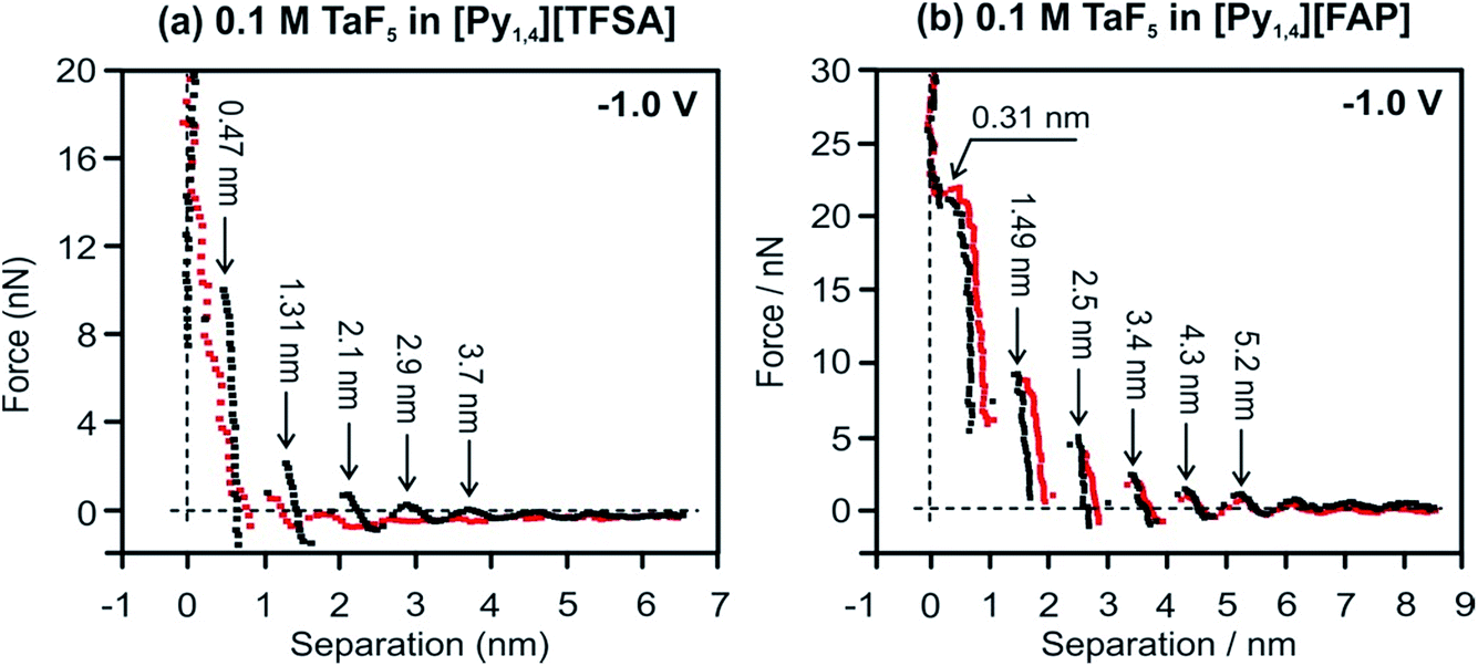 | ||
| Fig. 2 Force versus separation profiles for an AFM tip approaching the Au(111) surface at −1.0 V in (a) [Py1,4][TFSA] and (b) [Py1,4][FAP] in the presence (red curves) and in the absence (black curves) of 0.1 M TaF5. | ||
The important observation is that the addition of 0.1 M TaF5 does not alter the [Py1,4][FAP]/Au(111) interface (Fig. 2b). Both the width of the innermost layer and the push through force remain quite similar with and without TaF5. The width of the innermost layer is 0.31 nm, consistent with the size of [Py1,4]+.37 From these results we can conclude that TaF5 was expelled from the electrode surface in [Py1,4][FAP], while in [Py1,4][TFSA] the interfacial structure is disturbed by the addition of TaF5. Thus, TaF5 might interact in a different manner with [TFSA]− than with [FAP]−, which alters the interface.
Vibrational spectroscopy was performed to find changes in the bulk structure of ILs and TaF5–ILs. Fig. 3 shows the regions in which the changes can be observed in the Raman and IR spectra of the ILs on addition of TaF5.
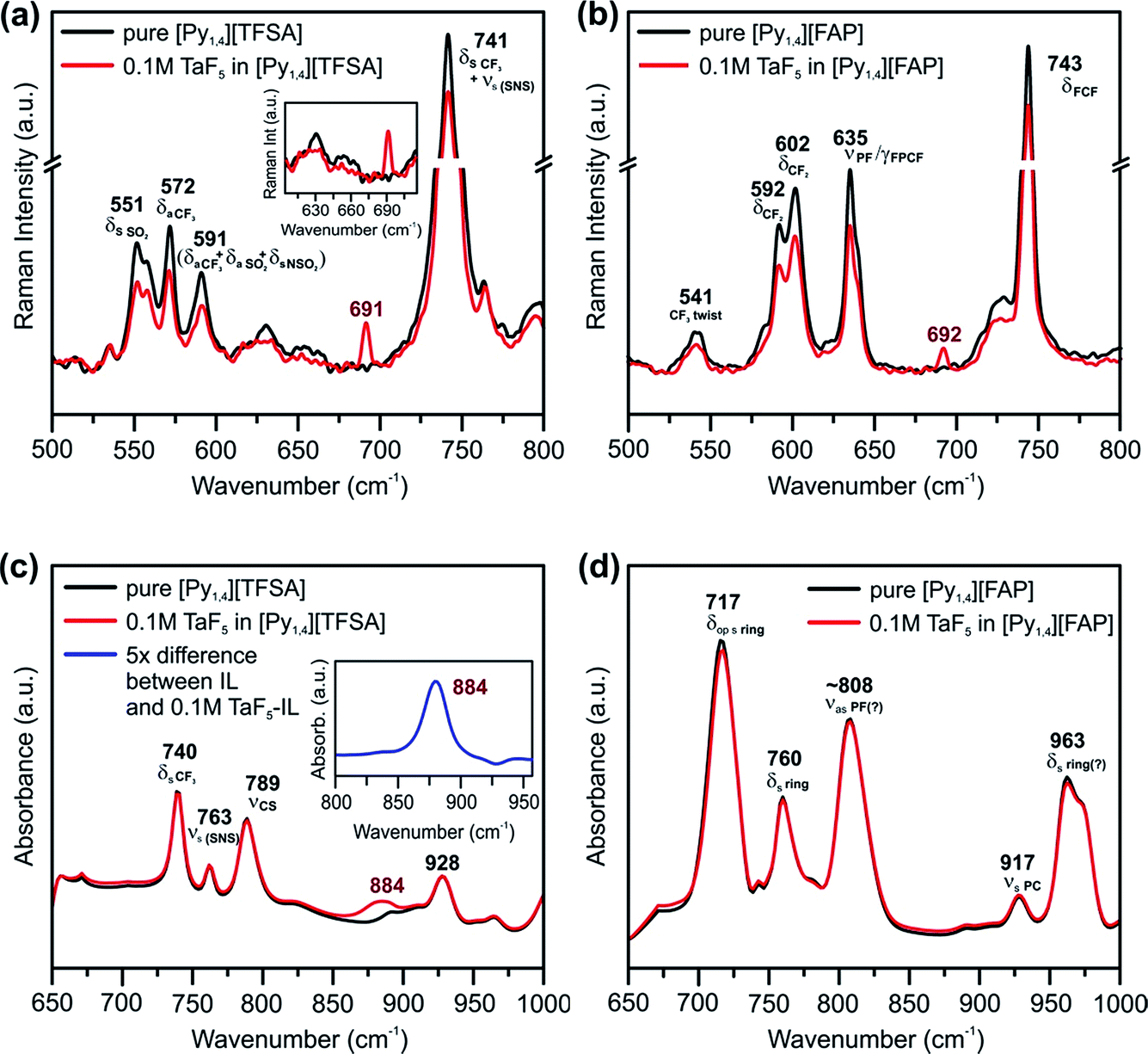 | ||
| Fig. 3 Raman spectra between the wavenumbers of 500 and 800 cm−1 in (a) [Py1,4][TFSA] and (b) [Py1,4][FAP] in the presence (red) and in the absence (black) of 0.1 M TaF5. Comparison of IR spectra between the wavenumbers of 650 and 1000 cm−1 of (c) [Py1,4][TFSA] and (d) [Py1,4][FAP] in the presence (red) and in the absence (black) of 0.1 M TaF5. The insets in (a) show Raman spectra between 605 and 710 cm−1, and in (c) show the difference IR spectrum of the solutions where the absorbance of [Py1,4][TFSA] is subtracted from the absorbance of 0.1 M TaF5–[Py1,4][TFSA] (blue, 5× magnification). The peaks are assigned based on ref. 52–55. | ||
Marginal changes are observed in the intensities of peaks related to the ILs, indicating a weak interaction of the TaF5 in them (Fig. 3a and b). However, we could neither observe new waves/peaks nor new shoulders except a new peak at ∼690 cm−1 for both ILs, which varies by 2 cm−1. This new peak could be related to TaF5–IL species.
In the IR spectra of TaF5–[Py1,4][TFSA] quite a broad and new peak appears at 884 cm−1 (Fig. 3c), which can not yet be assigned to a definite species. Apart from this, no recognizable changes have been observed in the IR spectrum for [Py1,4][FAP] upon addition of 0.1 M TaF5 (Fig. 3d). It is thus quite difficult to comment on the speciation/complexation based on the vibrational spectroscopy results alone and to correlate them with the observed changes in the in situ AFM results. Further investigations like 19F NMR of TaF5–ILs might be required to understand the solvation behavior of Ta species with ILs.
Gallium electrodeposition
Typical CVs of 0.2 M GaCl3 in [Py1,4][TFSA] and of 0.2 M GaCl3 in [Py1,4][TfO] on gold at RT are presented in Fig. 4a and b, respectively. Both GaCl3-containing ILs exhibit similar electrochemical behavior. The reduction processes at −0.9 V (for [Py1,4][TFSA]) and at −1.1 V (for [Py1,4][TfO]) are attributed to the deposition of Ga. The SEM micrographs show micrometer-thick layers of Ga deposited at −1.3 V for 1 hour (Fig. 4c and d). The crystal sizes of the obtained deposits varied in the ILs, and such changes are suggested to be correlated with the IL anion. The deposits made from [Py1,4][TFSA] consist of perfect spherical structures of 60–260 nm in diameter (Fig. 4c), whereas the average sizes of Ga deposits obtained from [Py1,4][TfO] are in the regime of 15 to 110 nm (Fig. 4d). | ||
| Fig. 4 CVs of 0.2 M GaCl3 (a) in [Py1,4][TFSA] and (b) in [Py1,4][TfO] on polycrystalline Au at RT. SEM micrographs of Ga electrodeposited at −1.3 V from (c) 0.2 M GaCl3/[Py1,4][TFSA] and (d) 0.2 M GaCl3/[Py1,4][TfO] at RT. | ||
Raman spectroscopy was used to investigate the influence of the anions of the ILs on the interaction/solvation of GaCl3. Fig. 5 shows the anion region of the Raman spectra of the ILs and their solutions with GaCl3, wherein significant changes can be identified. The peaks at 740 cm−1 (for pure [Py1,4][TFSA]) and at 757 cm−1 (for pure [Py1,4][TfO]) are assigned to a coupled symmetric CF3 bending and SNS bending modes of [TFSA]− (Fig. 5a, black curve), and to the CF3 symmetric bending mode of [TfO]− (Fig. 5b, black curve), respectively. On addition of GaCl3 a decrease in the IL peak intensities occurs. In the case of GaCl3–[Py1,4][TfO] an additional peak is seen at 767 cm−1 (Fig. 5b, red curve), and such a peak is not observed in GaCl3–[Py1,4][TFSA]. A decrease in intensity of the [TFSA]− and [TfO]− peaks at 740 and 757 cm−1, respectively, can be attributed to the interaction of GaCl3 with the anion of the ILs. Furthermore, new peaks were found at 366 and 363 cm−1 for GaCl3–[Py1,4][TFSA] and GaCl3–[Py1,4][TfO], respectively. For further analysis, the Raman modes of GaCl3 (or Ga2Cl6) and GaCl4− were compared with the stretching modes of GaCl3 in ILs. The Raman stretching modes (ν1 and ν3) of tetrachlorogallate complexes (GaCl4−) can be found at 346 and 386 cm−1, respectively.56 The Raman spectra of GaCl3/Ga2Cl6 at 140 °C have peaks at 168, 310, 344, 416, and 472 cm−1.57 However, we could not observe any such peaks in the GaCl3–ILs spectra indicating that either GaCl4− or GaCl3 (or its dimer) were absent in the solutions. Therefore, based on the Raman spectroscopy results we can summarize that anionic complexes/species of GaCl3 with the respective anions ([GaCl3A]−, where A = TFSA or TfO) might be formed in both of the ILs.
 | ||
| Fig. 5 Raman spectra between the wavenumbers of 200 and 800 cm−1 in (a) [Py1,4][TFSA] and (b) [Py1,4][TfO] in the presence (red) and in the absence (black) of 0.3 M GaCl3. The peaks are assigned based on ref. 54, 55 and 58. | ||
In situ AFM force–distance measurements were performed to investigate the interfacial structure of the pure ILs and in the presence of GaCl3 prior to the electrodeposition of Ga. A detailed study of the IL/Au(111) interface in [Py1,4][TFSA] has been reported previously.32,51 At negative electrode potentials multiple interfacial layers are present in the case of the pure ILs (Fig. 6, black curves). For [Py1,4][TfO], the width of the innermost layer (∼0.7 nm) does not change significantly by the decreasing of the electrode potential and corresponds well with the diameter of the IL ion pair.
 | ||
| Fig. 6 Force–distance profiles for an AFM tip approaching the Au(111) surface at (a) −0.8 V in [Py1,4][TFSA] and (b) at −1.0 V in [Py1,4][TfO] in the presence (red) and in the absence (black) of 0.2 M GaCl3. | ||
The structure of the innermost layer changes significantly with the addition of GaCl3. At −0.8 V only 3 solvation layers (at 0.2, 0.95 and 1.7 nm) can be detected in GaCl3–[Py1,4][TFSA] (Fig. 6a, red curve), while five steps can be found for GaCl3–[Py1,4][TfO] at −1.0 V (at 0.2, 0.55, 1.35, 2.5 and 3.5 nm) (Fig. 6b, red curve). In both ILs the innermost layer becomes thinner at the investigated electrode potentials as [GaCl3A]− species can present at the surface, which are responsible for Ga deposition. However, the interaction of the innermost layer with the gold surface differs in these two ILs. The addition of GaCl3 to [Py1,4][TFSA] weakens the interfacial structure, as the force required to rupture the innermost layer reduces to ∼7 nN. In contrast to [Py1,4][TFSA], the electroactive species in [Py1,4][TfO] strongly adsorbs to the electrode surface, wherein a ∼12 nN force is needed to rupture the innermost layer. Such differences in the adsorption structure of the Au(111)/GaCl3–IL interface can control the rate and growth (or particle sizes) of the Ga deposits.
Silicon electrodeposition
A few years ago, it was observed that the morphology and crystal size of Si deposits made electrochemically from ILs containing SiCl4 can be altered by changing the constituent ions.44 Si was electrodeposited from SiCl4 dissolved in three different ILs with the same cation, [Py1,4]+, but three different anions, (e.g. [Py1,4][TFSA], [Py1,4][TfO] and [Py1,4][FAP]). It was found that the number of reduction steps and the deposition potentials of Si differ upon changing the anion. Furthermore, in situ STM on Au(111) revealed a difference in the interfacial behaviour. IR spectroscopy analysis also showed that SiCl4 interacts differently with the ILs, leading to the formation of different silicon electroactive species.44 In the aforementioned examples the influence of the concentration of the solute on the structure of the IL/Au(111) interface was not investigated. In this section we focus on the influence of SiCl4 concentration on the Au(111)/[Py1,4][FAP] interface.The electrochemical behaviour of [Py1,4][FAP] at two different concentrations of 0.1 M and 0.25 M SiCl4 on Au(111) was investigated and the corresponding CVs are shown in Fig. 7a and b, respectively. In the cathodic regime, three reduction processes (C1–C3) can be obtained for 0.1 M SiCl4/[Py1,4][FAP]. The reduction waves C1 and C2 can be associated with the adsorption of SiCl4–IL species complexes. The bulk deposition of Si occurs at C3. The obtained result in this study is consistent with the previously reported results.44 On increasing the concentration of SiCl4 to 0.25 M, the magnitude of the reduction current increases. Furthermore, the potentials of the surface reduction processes were not affected by increasing the concentration of SiCl4 in the IL. However, the onset of Si electrodeposition is significantly shifted to more positive values when increasing the concentration of SiCl4 to 0.25 M. The Si deposits obtained from 0.1 M SiCl4–[Py1,4][FAP] on gold are quite thin and such thin layers have been observed only in STM investigations.44 However, a relatively thick layer of Si can be obtained from 0.25 M SiCl4–[Py1,4][FAP] on gold, which is surprising with respect to the results with TaF5, at a first glance. Therefore, we have investigated the interfacial structure of two different concentrations of SiCl4 in [Py1,4][FAP] on Au(111) using in situ AFM to probe interfacial processes at the conditions prior to the deposition of Si. Furthermore, to correlate the observed changes in the interfacial structure, we have monitored the changes in electroactive species of SiCl4/[Py1,4][FAP] by Raman spectroscopy.
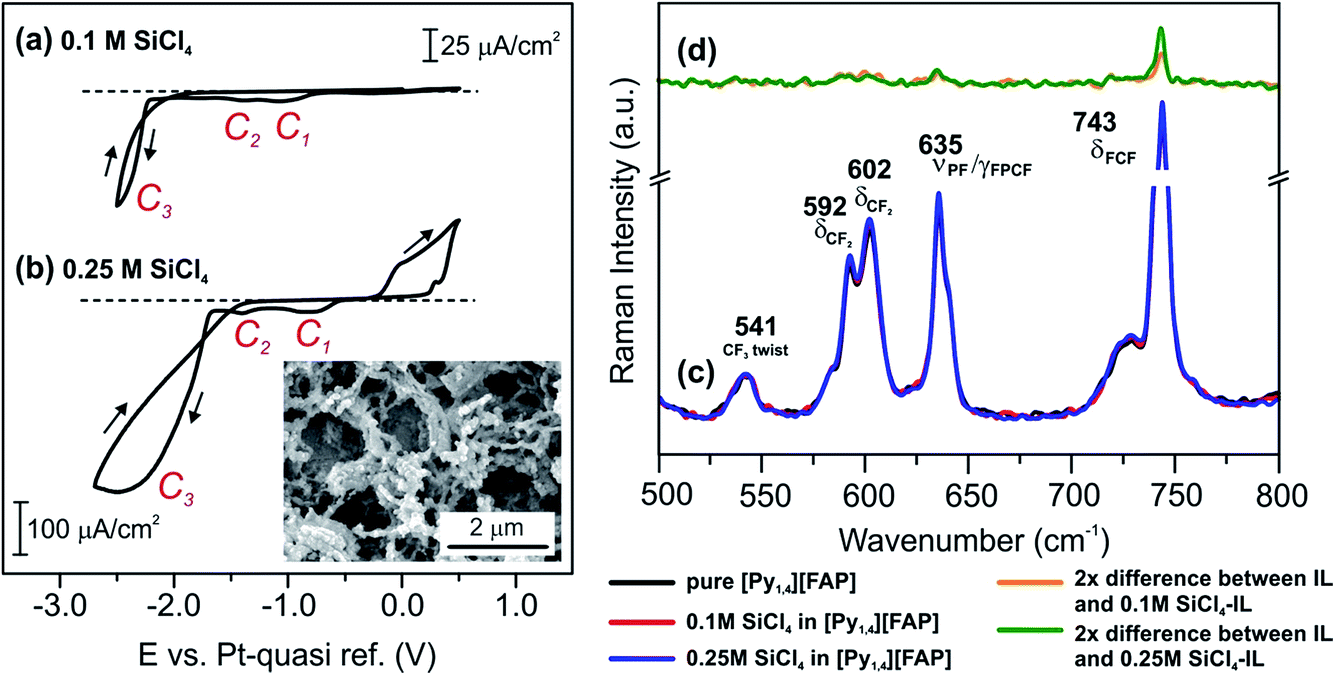 | ||
| Fig. 7 CVs of (a) 0.1 M SiCl4 and (b) 0.25 M SiCl4 in [Py1,4][FAP] on polycrystalline Au at 25 °C. The inset in (b) shows a SEM image of Si electrodeposited at −2.5 V from 0.25 M SiCl4 in [Py1,4][FAP]. (c) Raman spectra between 500 and 800 cm−1 in [Py1,4][FAP] (black), 0.1 M SiCl4–[Py1,4][FAP] (red) and 0.25 M SiCl4–[Py1,4][FAP] (blue). (d) Difference Raman spectra of the solutions, where the absorbance of [Py1,4][FAP] is subtracted from the 0.1 M SiCl4–[Py1,4][FAP] (orange) and 0.25 M SiCl4–[Py1,4][FAP] (green) absorbance (2× magnification). The peaks are assigned based on ref. 52 and 53. | ||
A comparison of the Raman spectra for the neat IL and its solutions with two different concentrations of SiCl4 (0.1 M and 0.25 M) is presented in Fig. 7c. We could neither observe new waves nor new peaks for the ILs containing two different concentrations of SiCl4. However, on addition of 0.1 M SiCl4, the intensity of the neat IL peak at 743 cm−1 increases, which is more pronounced at 0.25 M. This change in the intensity can be related to the formation of SiCl4–IL species. To find changes in the Raman spectra, we have analyzed the recorded ones by subtracting the absorbance of SiCl4/[Py1,4][FAP] from the absorbance of pure [Py1,4][FAP] (Fig. 7d). In the difference spectra, a rise in the intensity of the peak at 743 cm−1 can be noticed. At present, it is unclear why the intensity of this peak increases with the concentration of SiCl4 in this liquid. For a simple approximation, it might be due to weakening of the bending mode of C–F–C in the anion due to a possible interaction of SiCl4 with [FAP]−. Apart from such an intensity change, we could not observe any recognizable change either in the as-recorded spectra or in the difference spectra in this region of wavenumbers (500–800 cm−1).
In situ AFM was performed to understand the effect of SiCl4 concentration on the Au(111)/IL interface at the electrode potentials prior to the electrodeposition of Si. For the pure IL, it was already reported that at OCP and at slightly negative electrode potentials the width of the innermost layer is ∼0.3 nm, indicating the presence of [Py1,4]+ on the Au(111) surface.37 At more negative electrode potentials (at −1.5 V and −2.0 V) the cation layer can be so strongly bound to the surface that the AFM tip cannot displace them and thus probes only the anion layer at ∼0.6 nm (Fig. 8, black curves).51 However, by addition of SiCl4 the appearance of the AFM curves changes significantly. In the case of 0.1 M SiCl4–IL, only 3 layers (at 0.39, 0.85 and 1.9 nm) can be identified (Fig. 8a, red curve). The force required to rupture the layers is significantly reduced, with only 12 nN needed to displace the innermost layer. Furthermore, the innermost layer is only 0.39 nm wide, suggesting the presence of SiCl4–IL species at the surface. Interestingly, on increasing the concentration of SiCl4 to 0.25 M, only a double layer is seen at 0.61 nm (Fig. 8b, red curve). A similar double layer structure was reported for the Au(111)/[EMIm][TfO]–H2O interface.59 On increasing the water content to 50 vol%, the multi-layered IL/electrode interfacial structure was changed to a double layer structure, which consequently affected the rate and morphology of the electrodeposition of Zn.59 The presented results reveal that increasing the concentration of SiCl4 modifies the Au(111)/IL interface significantly, which can enhance the quality of the Si deposits.
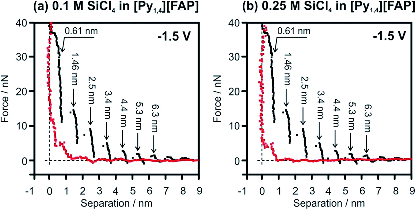 | ||
| Fig. 8 Force versus separation profiles for an AFM tip approaching the Au(111) surface at −1.5 V in [Py1,4][FAP] (black curves) and in [Py1,4][FAP] containing (a) 0.1 M and (b) 0.25 M of SiCl4 (red curves). | ||
The aforementioned examples show that the electrodeposition of metals (e.g. Ga and Ta) and semiconductors (e.g. Si) in ILs is not straightforward. On one side, the (chemical) structure of the IL has an influence on the EDL structure of the Au(111)/IL interface. On the other hand, the addition of precursors, which are required for the deposition processes, can also affect the structure of the electrode/IL interface. Furthermore, the nanostructure of interfacial layers can vary if the concentration of the precursor is increased, which might facilitate the deposition processes. These effects are unique for each IL and therefore cannot be generalized, if at all. An understanding of such interfacial and solvation effects is challenging and needs more fundamental experiments, ideally supported by interfacial theory.
Conclusions
The structure of the IL/Au(111) interface was analyzed in the presence of metal halides (TaF5 and GaCl3) and SiCl4 in ILs composed of [Py1,4]+ and different anions at electrode potentials just before the onset of electrodeposition. In situ AFM and vibrational spectroscopy were employed to evaluate the IL/solid interface and electroactive species, respectively, present in ILs and in the mixtures. The influence of the IL/electrode interfacial structure on the deposition process was discussed. Vibrational spectroscopy has revealed a marginal change in the spectra upon the addition of 0.1 M TaF5 to [Py1,4][TFSA] and to [Py1,4][FAP]. In situ AFM shows that, prior to the electrodeposition, the Ta-containing species are present at the IL/Au(111) interface in [Py1,4][TFSA] and can be further reduced to Ta. In contrast, in [Py1,4][FAP] the Ta species are expelled from the electrode surface, and therefore, the deposition of Ta from it fails completely. Gallium can be electrodeposited in both [Py1,4][TFSA] and [Py1,4][TfO] containing 0.2 M GaCl3. Although Raman spectroscopy reveals the formation of species/complexes like [GaCl4A]− (where A = TFSA or TfO) in both ILs, the obtained Ga layers possess different morphologies. In situ AFM studies indicate that the Au(111)/GaCl3–IL interfacial structure is different for both ILs, which consequently can affect the deposit characteristics. In the case of SiCl4–[Py1,4][FAP]/Au(111), it was found, in general, that the addition of SiCl4 weakens the IL/Au(111) interfacial structure. On increasing the concentration of SiCl4, instead of a multilayered interfacial structure typical for ILs, rather a classical double layer structure is observed prior to electrodeposition, which can facilitate the deposition process. The results obtained in the mentioned examples have shown that the structure of the IL/electrode interface is different for each system. In general, the structure of the IL/electrode interface has to change before the onset of the deposition process, which is crucial for discharge/charge processes to occur at it.Acknowledgements
The part of this work was financially supported by the Deutsche Forschungsgesellschaft (DFG) within Priority Program SPP 1708 (grant number: BO 4290/1-1) and by the Bundesministerium für Bildung und Forschung (BMBF) within the project LUZI (grant number: 03SF0499A).References
- M. Palacio and B. Bhushan, Tribol. Lett., 2010, 40, 247–268 CrossRef CAS.
- A. Somers, P. Howlett, D. MacFarlane and M. Forsyth, Lubricants, 2013, 1, 3–21 CrossRef.
- F. Endres, A. P. Abbott and D. R. MacFarlane, Electrodeposition from Ionic Liquids, Wiley-VCH Verlag GmbH & Co. KGaA, Weinheim, 2nd edn, 2017 Search PubMed.
- M. Watanabe, M. L. Thomas, S. Zhang, K. Ueno, T. Yasuda and K. Dokko, Chem. Rev., 2017, 117, 7190–7239 CrossRef CAS PubMed.
- J. Dupont and L. Kollár, Ionic Liquids (ILs) in Organometallic Catalysis, Springer, Berlin, Heidelberg, 2015 Search PubMed.
- M. Gouy, J. Phys. Theor. Appl., 1910, 9, 457–468 CrossRef.
- D. L. Chapman, Philos. Mag., Ser. 5, 1913, 25, 475–481 CrossRef.
- O. Stern, Z. Elektrochem. Angew. Phys. Chem., 1924, 30, 508–516 CAS.
- M. Z. Bazant, B. D. Storey and A. A. Kornyshev, Phys. Rev. Lett., 2011, 106, 046102 CrossRef PubMed.
- A. A. Kornyshev, J. Phys. Chem. B, 2007, 111, 5545–5557 CrossRef CAS PubMed.
- M. V. Fedorov and A. A. Kornyshev, J. Phys. Chem. B, 2008, 112, 11868–11872 CrossRef CAS PubMed.
- R. M. Lynden-Bell, A. I. Frolov and M. V. Fedorov, Phys. Chem. Chem. Phys., 2012, 14, 2693–2701 RSC.
- A. A. Kornyshev and R. Qiao, J. Phys. Chem. C, 2014, 118, 18285–18290 CAS.
- M. V. Fedorov, N. Georgi and A. A. Kornyshev, Electrochem. Commun., 2010, 12, 296–299 CrossRef CAS.
- C. Merlet, D. T. Limmer, M. Salanne, R. Van Roij, P. A. Madden, D. Chandler and B. Rotenberg, J. Phys. Chem. C, 2014, 118, 18291–18298 CAS.
- M. V. Fedorov and A. A. Kornyshev, Chem. Rev., 2014, 114, 2978–3036 CrossRef CAS PubMed.
- S. Baldelli, Acc. Chem. Res., 2008, 41, 421–431 CrossRef CAS PubMed.
- Y. Jeon, J. Sung, W. Bu, D. Vaknin, Y. Ouchi and D. Kim, J. Phys. Chem. C, 2008, 112, 19649–19654 CAS.
- C. S. Santos and S. Baldelli, J. Phys. Chem. B, 2009, 113, 923–933 CrossRef CAS PubMed.
- R. G. Horn, D. F. Evans and B. W. Ninham, J. Phys. Chem., 1988, 92, 3531–3537 CrossRef CAS.
- S. Perkin, T. Albrecht and J. Klein, Phys. Chem. Chem. Phys., 2010, 12, 1243–1247 RSC.
- S. Perkin, L. Crowhurst, H. Niedermeyer, T. Welton, A. M. Smith and N. N. Gosvami, Chem. Commun., 2011, 47, 6572–6574 RSC.
- M. Mezger, S. Schramm, H. Schröder, H. Reichert, M. Deutsch, E. J. De Souza, J. S. Okasinski, B. M. Ocko, V. Honkimaki and H. Dosch, J. Chem. Phys., 2009, 131, 094701 CrossRef PubMed.
- C. Hardacre, J. D. Holbrey, C. L. Mullan, T. G. A. Youngs and D. T. Bowron, J. Chem. Phys., 2010, 133, 074510 CrossRef PubMed.
- A. Triolo, O. Russina, H.-J. Bleif and E. Di Cola, J. Phys. Chem. B, 2007, 111, 4641–4644 CrossRef CAS PubMed.
- T. L. Greaves, D. F. Kennedy, S. T. Mudie and C. J. Drummond, J. Phys. Chem. B, 2010, 114, 10022–10031 CrossRef CAS PubMed.
- R. Hayes, S. Imberti, G. G. Warr and R. Atkin, Phys. Chem. Chem. Phys., 2011, 13, 3237–3247 RSC.
- M. Mezger, H. Schröder, H. Reichert, S. Schramm, J. S. Okasinski, S. Schöder, V. Honkimäki, M. Deutsch, B. M. Ocko, J. Ralston, M. Rohwerder, M. Stratmann and H. Dosch, Science, 2008, 322, 424–428 CrossRef CAS PubMed.
- A. Elbourne, S. McDonald, K. Voïchovsky, F. Endres, G. G. Warr and R. Atkin, ACS Nano, 2015, 9, 7608–7620 CrossRef CAS PubMed.
- T. Carstens, R. Gustus, O. Höfft, N. Borisenko, F. Endres, H. Li, R. J. Wood, A. J. Page and R. Atkin, J. Phys. Chem. C, 2014, 118, 10833–10843 CAS.
- R. Atkin, N. Borisenko, M. Drüschler, F. Endres, R. Hayes, B. Huber and B. Roling, J. Mol. Liq., 2014, 192, 44–54 CrossRef CAS.
- R. Atkin, S. Zein El Abedin, R. Hayes, L. H. S. Gasparotto, N. Borisenko and F. Endres, J. Phys. Chem. C, 2009, 113, 13266–13272 CAS.
- N. Borisenko, S. Zein El Abedin and F. Endres, ChemPhysChem, 2012, 13, 1736–1742 CrossRef CAS PubMed.
- T. Carstens, R. Hayes, S. Zein El Abedin, B. Corr, G. B. Webber, N. Borisenko, R. Atkin and F. Endres, Electrochim. Acta, 2012, 82, 48–59 CrossRef CAS.
- A. Elbourne, J. Sweeney, G. B. Webber, E. J. Wanless, G. G. Warr, M. W. Rutland and R. Atkin, Chem. Commun., 2013, 49, 6797–6799 RSC.
- F. Endres, N. Borisenko, S. Zein El Abedin, R. Hayes and R. Atkin, Faraday Discuss., 2012, 154, 221–233 RSC.
- R. Hayes, N. Borisenko, M. K. Tam, P. C. Howlett, F. Endres and R. Atkin, J. Phys. Chem. C, 2011, 115, 6855–6863 CAS.
- F. Endres, O. Höfft, N. Borisenko, L. H. Gasparotto, A. Prowald, R. Al-Salman, T. Carstens, R. Atkin, A. Bund and S. Zein El Abedin, Phys. Chem. Chem. Phys., 2010, 12, 1724–1732 RSC.
- H. Li, F. Endres and R. Atkin, Phys. Chem. Chem. Phys., 2013, 15, 14624–14633 RSC.
- H. Li, R. J. Wood, F. Endres and R. Atkin, J. Phys.: Condens. Matter, 2014, 26, 284115 CrossRef PubMed.
- S. Zein El Abedin, E. M. Moustafa, R. Hempelmann, H. Natter and F. Endres, ChemPhysChem, 2006, 7, 1535–1543 CrossRef CAS PubMed.
- P. Eiden, Q. Liu, S. Zein El Abedin, F. Endres and I. Krossing, Chem.–Eur. J., 2009, 15, 3426–3434 CrossRef CAS PubMed.
- Z. Liu, S. Z. El Abedin and F. Endres, Phys. Chem. Chem. Phys., 2015, 17, 15945–15952 RSC.
- G. Pulletikurthi, A. Lahiri, T. Carstens, N. Borisenko, S. Zein El Abedin and F. Endres, J. Solid State Electrochem., 2013, 17, 2823–2832 CrossRef CAS.
- P. Giridhar, A. M. Elbasiony, S. Zein El Abedin and F. Endres, ChemElectroChem, 2014, 1, 1549–1556 CrossRef CAS.
- Z. Liu, T. Cui, T. Lu, M. Shapouri Ghazvini and F. Endres, J. Phys. Chem. C, 2016, 120, 20224–20231 CAS.
- R. Al-Salman and F. Endres, J. Mater. Chem., 2009, 19, 7228–7231 RSC.
- A. Lahiri, N. Borisenko, M. Olschewski, R. Gustus, J. Zahlbach and F. Endres, Angew. Chem., Int. Ed., 2015, 54, 11870–11874 CrossRef CAS PubMed.
- N. Borisenko, A. Ispas, E. Zschippang, Q. Liu, S. Zein El Abedin, A. Bund and F. Endres, Electrochim. Acta, 2009, 54, 1519–1528 CrossRef CAS.
- A. Ispas, B. Adolphi, A. Bund and F. Endres, Phys. Chem. Chem. Phys., 2010, 12, 1793–1803 RSC.
- T. Carstens, A. Ispas, N. Borisenko, R. Atkin, A. Bund and F. Endres, Electrochim. Acta, 2016, 197, 374–387 CrossRef CAS.
- I. V. Voroshylova, F. Teixeira, R. Costa, C. M. Pereira and M. N. D. S. Cordeiro, Phys. Chem. Chem. Phys., 2016, 18, 2617–2628 RSC.
- J. X. Mao and K. Damodaran, Ionics, 2015, 21, 1605–1613 CrossRef CAS.
- A. M. Moschovi, S. Ntais, V. Dracopoulos and V. Nikolakis, Vib. Spectrosc., 2012, 63, 350–359 CrossRef CAS.
- M. Castriota, T. Caruso, R. G. Agostino, E. Cazzanelli, W. A. Henderson and S. Passerini, J. Phys. Chem. A, 2005, 109, 92–96 CrossRef CAS PubMed.
- L. A. Woodward and A. A. Nord, J. Chem. Soc., 1956, 3721–3722 RSC.
- I. R. Beattie and J. R. Horder, J. Chem. Soc. A, 1969, 2655–2659 RSC.
- D. H. Johnston and D. F. Shriver, Inorg. Chem., 1993, 32, 1045–1047 CrossRef CAS.
- T. Cui, A. Lahiri, T. Carstens, N. Borisenko, G. Pulletikurthi, C. Kuhl and F. Endres, J. Phys. Chem. C, 2016, 120, 9341–9349 CAS.
| This journal is © The Royal Society of Chemistry 2018 |