
 Open Access Article
 This Open Access Article is licensed under a Creative Commons Attribution-Non Commercial 3.0 Unported Licence
Textured interfaces in monolithic perovskite/silicon tandem solar cells: advanced light management for improved efficiency and energy yield†
Marko
Jošt
 *a,
Eike
Köhnen
a,
Anna Belen
Morales-Vilches
b,
Benjamin
Lipovšek
c,
Klaus
Jäger
d,
Bart
Macco
e,
Amran
Al-Ashouri
a,
Janez
Krč
c,
Lars
Korte
e,
Bernd
Rech
e,
Rutger
Schlatmann
b,
Marko
Topič
c,
Bernd
Stannowski
b and
Steve
Albrecht
*a
*a,
Eike
Köhnen
a,
Anna Belen
Morales-Vilches
b,
Benjamin
Lipovšek
c,
Klaus
Jäger
d,
Bart
Macco
e,
Amran
Al-Ashouri
a,
Janez
Krč
c,
Lars
Korte
e,
Bernd
Rech
e,
Rutger
Schlatmann
b,
Marko
Topič
c,
Bernd
Stannowski
b and
Steve
Albrecht
*a
aYoung Investigator Group Perovskite Tandem Solar Cells, Helmholtz-Zentrum Berlin für Materialien und Energie GmbH, Kekuléstraße 5, 12489 Berlin, Germany. E-mail: marko.jost@helmholtz-berlin.de; steve.albrecht@helmholtz-berlin.de
bPVcomB, Helmholtz Zentrum Berlin für Materialien und Energie, Schwarzschildstr. 3, 12489 Berlin, Germany
cUniversity of Ljubljana, Faculty of Electrical Engineering, Tržaška 25, 1000 Ljubljana, Slovenia
dYoung Investigator Group Nano-SIPPE, Helmholtz-Zentrum Berlin für Materialien und Energie GmbH, Albert-Einstein-Straße 16, 12489 Berlin, Germany
eInstitute for Silicon Photovoltaics, Helmholtz-Zentrum Berlin für Materialien und Energie GmbH, Kekuléstraße 5, 12489 Berlin, Germany
First published on 25th October 2018
Abstract
Efficient light management in monolithic perovskite/silicon tandem solar cells is one of the prerequisites for achieving high power conversion efficiencies (PCEs). Textured silicon wafers can be utilized for light management, however, this is typically not compatible with perovskite solution processing. Here, we instead employ a textured light management (LM) foil on the front-side of a tandem solar cell processed on a wafer with a planar front-side and textured back-side. This way the PCE of monolithic, 2-terminal perovskite/silicon-heterojunction tandem solar cells is significantly improved from 23.4% to 25.5%. Furthermore, we validate an advanced numerical model for our fabricated device and use it to optically optimize a number of device designs with textures at different interfaces with respect to the PCE and energy yield. These simulations predict a slightly lower optimal bandgap of the perovskite top cell in a textured device as compared to a flat one and demonstrate strong interdependency between the bandgap and the texture position in the monolithic stack. We estimate the PCE potential for the best performing both-side textured device to be 32.5% for a perovskite bandgap of 1.66 eV. Furthermore, the results show that under perpendicular illumination conditions, for optimized designs, the LM foil on top of the cell performs only slightly better than a flat anti-reflective coating. However, under diffuse illumination, the benefits of the LM foil are much greater. Finally, we calculate the energy yield for the different device designs, based on true weather data for three different locations throughout the year, taking direct as well as diffuse illumination fully into account. The results further confirm the benefits of front-side texture, even more for BIPV applications. Overall, devices built on a both-side textured silicon wafer perform best. However, we show that devices with textured LM foils on the cell's front-side are a highly efficient alternative.
Broader contextMetal halide perovskite materials are perfectly suitable for a tandem solar cell due to their excellent optoelectronic properties and tunable bandgap. An excellent combination as an add-on to existing fabrication routes for conventional, market dominating silicon solar cells, it has the potential to increase the power conversion efficiency significantly while only marginally increasing the production costs. To push the power conversion efficiency (PCE) of the monolithic perovskite/silicon tandem devices further, efficient light management, including textured interfaces, is of utmost importance. In our work, we present an efficient monolithic perovskite/silicon-heterojunction tandem solar cell with a 25.5% PCE, enabled by a textured light management (LM) foil, applied at the front-side. By building an experimentally verified optical model, we are able to determine the losses in the fabricated device and use it to optically optimize and estimate the PCE of a number of configurations with a texture at different positions. Our simulations show that a 32.5% PCE is realistically achievable with a 1000 nm thick perovskite with a bandgap of 1.66 eV on top of a both-side textured silicon wafer. By further extending our model to include diffuse light conditions, we are able to predict the energy yield of the configurations under investigation. Our results highlight the beneficial effect of a front-side texture under outdoor conditions, and even more when building integrated photovoltaics (BIPV) are considered. |
Introduction
Perovskite based tandem solar cells have attracted strong research interest due to their promise to boost the power conversion efficiency (PCE) at reasonable costs1–3 while being compatible with existing silicon technology. Silicon-heterojunction (SHJ) solar cells are widely used as bottom cells due to the very high PCE potential of such a combination; efficiencies above 25% and 26%, respectively, in monolithic 2-terminal and 4-terminal configuration have already been shown.4–7 Further improvements are possible by e.g. implementing optimized light management schemes into the device architecture.In monocrystalline silicon solar cells, randomly distributed pyramids with an angle of 54.7° and a few micrometers in pyramid height and base length are usually implemented for efficient light in-coupling and light trapping. These pyramids are wet-chemically etched into the front- and back-sides of the wafer.8,9 While the front-side texture reduces reflection over the whole wavelength range, the back-side texture enhances photocurrent generation in the near infrared wavelength region. Textured silicon cells have also been used for tandem architectures. The back-side texture does not affect wet-chemical processing of a perovskite cell on the polished front-side. However, until recently textured front-sides were not suitable for the deposition of perovskite layers with spin-coating that gives the highest efficiencies and process control to date. Despite first proofs of concept shown with smooth nano-textures,10 full11 or hybrid5 vacuum perovskite deposition is needed to implement conformal coatings of the perovskite top cell. Alternatively, planar anti-reflection (AR) coatings, such as LiF or MgF2, or textured light management (LM) foils can yield further gains in photocurrents. By introducing a texture on the planar front-side of the device,12–14 the LM foil has two effects: it reduces reflection and enables enhanced light trapping by backscattering the upward propagating light at the LM foil/air interface.14 Being compatible with solution processing, the LM foils are thus perfectly suited for improving light management for this tandem application. Additionally, use of the LM foil allows one to freely choose a texture of any shape, such as nanocavities/microlenses15 or periodic inverted pyramids.16 Having the front- and back-side of the tandem textured differently opens up new routes for further optical optimization.
In Fig. 1 we highlight five monolithic 2-terminal device architectures with different light management strategies [device designs (A, B, C, D and E)]. The main milestones in tandem development with the authors and PCE reached by implementing textures at different interfaces in the devices are also denoted. The simplest device design without any textured interfaces is design A. However, the first monolithic perovskite/silicon tandem was built in early 2015 on a back-side textured homojunction silicon substrate [device (B)] with a PCE of 13.7%.17 Soon, the community turned to SHJ bottom cells due to their superior performance and ease of tandem integration. The first monolithic perovskite/SHJ tandem solar cell was built soon after, utilizing a both-side polished silicon wafer [device (A)] resulting in a PCE of 18%.18 The PCE was soon improved to 21.2% by using a textured LM foil instead of a planar AR coating on top of the device [device (E)] by Werner et al.12 The following tandem cells utilized a back-side textured silicon wafer [device (B)]. With this design PCEs of 20.5% in 201619 and 23.6% in 201720 were achieved. Recently, a cell with a 25.2% PCE was certified; the device was fabricated in a collaboration between Helmholtz-Zentrum Berlin (HZB), University of Oxford and Oxford PV using design (B).4,21 Simultaneously, for the first time a both-side textured silicon bottom cell with a perovskite top cell processed directly on the texture [device (D)] was reported by Sahli et al. with a 25.2% certified PCE as well.5 To fabricate the top cell on a textured substrate, they utilized a hybrid process in which first the inorganic compounds were conformally evaporated and afterwards the organic compounds were spin-coated on top. Interestingly, the combination of a back-side textured device with a textured LM foil on top of the flat front side [device (C)] has not yet been experimentally tested despite promising results on a fully flat tandem device12 and silicon single-junction cells.22 A similar approach has already been investigated in detail for perovskite single junction cells by some of the authors of this paper.13
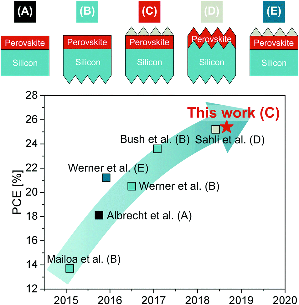 | ||
| Fig. 1 Different reported texture configurations for experimentally realized perovskite/silicon tandem solar cells including the main developments with the authors and PCE as denoted in the figure. Device schematics indicate where the texture position is located. Device (A) is a fully flat device. Device (B) is a back-side textured device. Device (C) is a back-side textured device with the LM foil as experimentally developed in this work. Device (D) is a both-side textured device whereas device (E) is a fully flat device with the LM foil. If the device has no LM foil, a planar AR coating is considered (not depicted in the schematics for clarity). | ||
In parallel, many papers have already investigated a wide range of perovskite/SHJ tandem solar cell designs using numerical optical simulations.23–28 Indeed, improved optics of the tandem devices are necessary to achieve efficiencies above 30%.26,28 Simulations were mostly focused on the effect of different perovskite bandgaps on efficiency,25–27 even for multiple (>2) junctions,27 and the effect of texturing.23,24 The detailed balance limit for a 2-terminal perovskite/silicon tandem states the optimal perovskite bandgap to be 1.73 eV.29 However, this does not include the full device stack. The validation of device simulations for actual tandem solar cells – including realistic optical properties also of the contact layers – by experiments is rarely reported,30 since the experimental and simulation papers are typically not closely related. Therefore, studies on optimal perovskite bandgap and solar cell layer thicknesses can be contradictive; some suggest an optimal perovskite bandgap above 1.7 eV,25,26 while some suggest a lower bandgap around 1.65 eV is sufficient.28,31 Additionally, those simulations assumed planar interfaces and neglected possible optical changes brought about by introducing textured surface designs at the front or rear side. Therefore, it is not yet clear what the perfect bandgap for the perovskite top-cell in different device designs is.
Analysis is usually done for perpendicular, direct illumination, as is the standard in optical simulations and for standard testing conditions. In outdoor applications under realistic weather, spectral and sun position conditions, most of the light does not enter the cell perpendicularly, especially if no axial tracking is applied. Depending on location, the ratio between diffuse and direct illumination spectra also differs.32 This makes yearly energy yield a key parameter in the analysis of photovoltaic device performance. While the first reports are promising, it is not yet clear whether a 2-terminal design can outperform the best single junction in reality.28,33,34 Thus, a more relevant energy yield analysis is necessary that includes light trapping, especially for diffuse incident light or oblique illumination in the morning or late afternoon.
In our contribution, we therefore focus on textured interfaces in monolithic perovskite/SHJ solar cells in both simulation and experiment. First, we fabricate a back-side textured tandem device in a p–i–n top cell configuration and investigate the effect of applying a textured LM foil on top of the flat front of the tandem solar cell. This way we are able to use the high perovskite film quality of the spin-coated perovskite while at the same time still implement efficient light management in the device. To evaluate the potential of our device, we perform optical simulations based on experimentally relevant input parameters. We analyse the tandems with texture at different interfaces, as illustrated in Fig. 1. We optimize the layer stack and perovskite bandgap for each of the designs and estimate the realistically achievable efficiency. By extending our model to include diffuse light in calculations, we are able to estimate the energy yield of all the designs and their improvements due to the texture under realistic environmental conditions. Our results highlight the significance of the front-side texture. We show and confirm that by applying a LM foil on top of a fabricated device, we can keep the benefits of the best performing spin-coated perovskite devices while implementing efficient light trapping. With that, our results give indications of the highest efficiencies obtainable in perovskite/SHJ tandem devices with different device designs and present detailed guidelines on how to reach them.
Experimental
Based on our recent simulation results,26 we adopt in our experimental tandem development the so called “inverted” architecture with a rear emitter a-Si:H (p)/c-Si (n) SHJ and a p–i–n perovskite top cell that shows low parasitic absorption losses in the front contact. Fig. 2 displays the schematic of the fabricated monolithic perovskite/SHJ tandem device and a cross section SEM image of the top cell. In addition to the top cell SEM image, Fig. S1 (ESI†) shows the cross-section SEM of the back-side of the bottom cell. We utilized a back-side textured and front-side polished rear emitter SHJ bottom cell, which has been optimized for the tandem architecture as reported previously.35 We replaced the n-doped amorphous silicon a-Si:H (n) layer of the front surface field (FSF) by a n-doped nanocrystalline silicon oxide layer, nc-SiOx:H. This layer improves light in-coupling in the bottom silicon cell by reducing the reflection at the ITO/nc-SiOx:H interface as compared to ITO/a-Si:H (n). On top of the FSF, a thin ITO recombination layer connecting both sub cells is deposited. The top cell is fabricated in the “inverted” design, in which the p-type contact is deposited on the interconnection layer. Here we utilized the p-type polymer PTAA36,37 as the hole selective layer. As a perovskite absorber we selected a multiple cation, multiple halide composition: Cs0.05(MA0.17FA0.83)Pb1.1(I0.83Br0.17)3, first reported by Saliba et al.38 The n-type top contact is formed via thermally evaporated fullerene, C60, a tin oxide (SnO2) buffer layer deposited via atomic layer deposition (ALD) and RF sputtered indium zinc oxide (IZO). Finally, a silver contact frame is evaporated to enable a good electrical contact and current collection. The silver on the front-side partially covers the edge of the area defined by the overlap of the patterned TCO layers throughout the full device stack and the metallization area on the cell's back-side which is 1 cm2. The active area of the final device is 0.81 cm2 as defined by the inner opening of the top metal frame. The cells have then been measured using a shadow mask with an opening of either 0.77 cm2 (mask area ≤ active area) or 1 cm2 (mask area > active area) as is discussed in further detail below.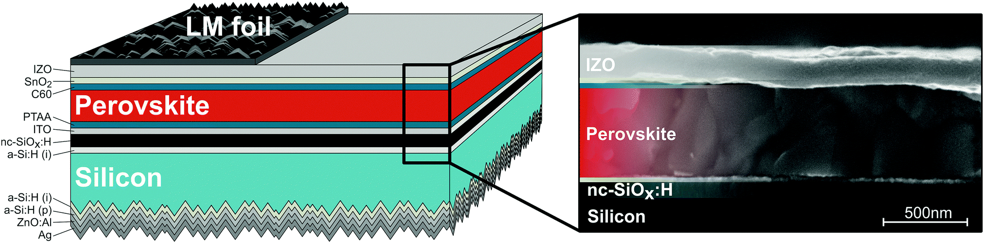 | ||
| Fig. 2 Tandem solar cell device schematics of the experimentally realized architecture and SEM cross section image of the top cell with the layers as indicated. | ||
To improve light management in the fabricated tandem device with a planar front side, we apply a textured light management (LM) foil [device (C) in Fig. 1]. As a master for the LM foil fabrication by an UV nanoimprint lithography process,13 we used a KOH-etched silicon wafer with similar texture as our silicon bottom cell. Consequently, the top surface of the LM foil and our device is the same as it would be for the tandem potentially built on a both-side textured silicon wafer. The 100 μm thick LM foil was processed on a glass substrate and attached on the front-side using an index matching liquid (Norland Products Inc., n = 1.5). This configuration already resembles the module application where the front-side flat device would be encapsulated by glass (albeit thicker – 200 μm vs. 3.2 mm) covered by the LM foil. The LM foil fabrication details can be found in our previous paper.13 The tandem device fabrication process is described in detail in the Methods section.
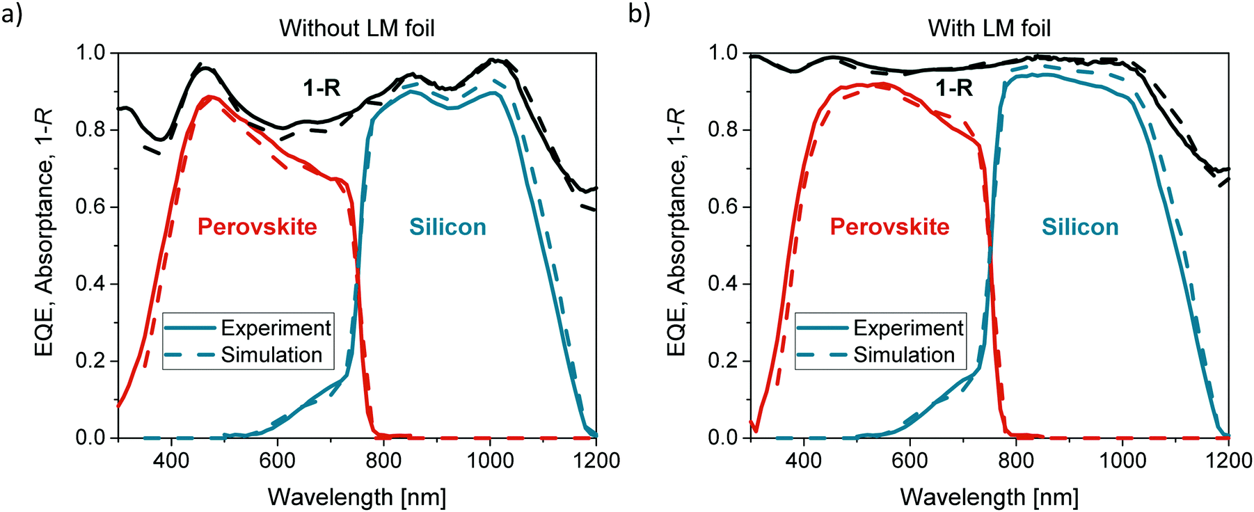
Fig. 3a shows the EQE and 1-reflectance (1-R) of the best fabricated monolithic perovskite/SHJ tandem devices without and with LM foil as well as their AM 1.5G integrated photocurrent densities JSC_EQE calculated from the EQE spectra. A significant increase in the photocurrent density due to the LM foil can be observed for both sub cells: by more than 2 mA cm−2 for the top cell and by 0.92 mA cm−2 for the bottom cell. This improvement is higher than expected from single-junction cells13 due to a more detrimental air/IZO (nair![[thin space (1/6-em)]](https://www.rsc.org/images/entities/char_2009.gif) :nIZO = 1:∼2) interface in the tandem compared to the air/glass (nair:nglass = 1:1.5) interface in the single-junction device. The total reflection is reduced to below 5% in the 300–1000 nm range. Overall, the reflective losses are only 2.48 mA cm−2 in the wavelength range of interest (300–1200 nm), as compared to 6.13 mA cm−2 for the cell without the LM foil. The optimized optical design of our stack is further confirmed by the very low parasitic losses. Less than 8% is lost in other layers for wavelengths between 470 and 1000 nm (<5% between 500 and 900 nm). Only in the UV region the optical losses are higher due to absorption in IZO, SnO2 and C60 layers in the top contact, as well as above 1050 nm by absorption in the back contact. The fabricated solar cell without any light trapping foil is well current matched at ca. 18 mA cm−2. Including the LM foil induces a strong current mismatch of more than 1 mA cm−2 between the top and bottom cell, limited by the silicon bottom cell. Thus there is more efficiency to gain by further optical optimization, which will be discussed in the simulation section.
:nIZO = 1:∼2) interface in the tandem compared to the air/glass (nair:nglass = 1:1.5) interface in the single-junction device. The total reflection is reduced to below 5% in the 300–1000 nm range. Overall, the reflective losses are only 2.48 mA cm−2 in the wavelength range of interest (300–1200 nm), as compared to 6.13 mA cm−2 for the cell without the LM foil. The optimized optical design of our stack is further confirmed by the very low parasitic losses. Less than 8% is lost in other layers for wavelengths between 470 and 1000 nm (<5% between 500 and 900 nm). Only in the UV region the optical losses are higher due to absorption in IZO, SnO2 and C60 layers in the top contact, as well as above 1050 nm by absorption in the back contact. The fabricated solar cell without any light trapping foil is well current matched at ca. 18 mA cm−2. Including the LM foil induces a strong current mismatch of more than 1 mA cm−2 between the top and bottom cell, limited by the silicon bottom cell. Thus there is more efficiency to gain by further optical optimization, which will be discussed in the simulation section.
 | ||
| Fig. 3 (a) EQE measurement of the fabricated tandem devices without and with the LM foil. Integrated JSC_EQE values as well as the current lost due to reflection are shown. The red spectrum denotes perovskite, blue silicon and grey reflection. (b) Corresponding JV characteristics of the fabricated tandem device without (blue) and with the LM foil (red) measured with an aperture mask just slightly smaller than the active area that will underestimate the measured current as described in the text. | ||
The corresponding JV characteristics (measured with a mask area ≤ active area) without and with the LM foil are shown in Fig. 3b. The inset in the figure illustrates the illumination conditions. The respective performance metrics are summarized in Table 1. Applying the LM foil leads to a significantly higher short-circuit current density JSC by more than 1 mA cm−2, an increase from 17.3 to 18.5 mA cm−2. The open-circuit voltage (VOC) depends logarithmically on the photocurrent and is thus not affected by the LM foil with a value of 1.76 V. The tandem cell with the LM foil is current mismatched and therefore the fill factor (FF) in reverse scan is potentially enhanced from 76.4% to above 78.5% with the LM foil due to the limiting influence of the Si subcell.39 As a result, the power conversion efficiency (PCE) of 23.4% for the tandem device without light management is increased to 25.5% with the LM foil, in the reverse scan. The measured PCE is among the highest reported values for 2-terminal perovskite/silicon tandem solar cells. Note that the measured JSC using a mask just slightly smaller than the active area (mask area ≤ active area) will underestimate the measured JSC, as can be seen in Fig. S2 in the ESI.† Compared to the value from integrated small spot EQE spectra, in which all of the incident light is captured by the active area, in JV measurements almost 0.4 mA cm−2 is lost by scattering out of the active area due to the textured LM foil. Utilizing a larger mask that enables us to compensate for this effect, as shown in Fig. S3 (ESI†), a higher photocurrent and thus PCE are measured; 19.4 mA cm−2 and 26.5%, respectively. This value serves as an upper limit for the potential tandem efficiency when being integrated into a module with glass encapsulation where light scattering into the active area from outside the cell is enhanced due to backsheet, frame and grid reflection and subsequent light trapping. As slight effects of hysteresis are present, especially for the current matched device without the LM foil, we measured maximum power point (MPP) tracking. The PCEMPP are stable without and with the LM foil for over 5 minutes (Fig. S4, ESI†), displaying a good short-term stability of the fabricated device. For the device with the LM foil, the stabilized power output is very close to the reverse scan.
| Illumination condition | Without LM foil | With LM foil (design C) | |||
|---|---|---|---|---|---|
| Forward | Reverse | Forward | Reverse | ||
| (1) mask area ≤ active area | J SC [mA cm−2] | 17.3 | 17.3 | 18.5 | 18.5 |
| V OC [V] | 1.76 | 1.76 | 1.76 | 1.76 | |
| FF [%] | 75.7 | 76.4 | 78.3 | 78.5 | |
| PCE [%] | 23.1 | 23.4 | 25.4 | 25.5 | |
| (2) Small beam spot EQE | J SC_EQE [mA cm−2] | Perovskite | 17.95 | Perovskite | 20.21 |
| Silicon | 17.96 | Silicon | 18.81 | ||
| (3) Mask area > active area | J SC [mA cm−2] | 17.1 | 17.1 | 19.4 | 19.4 |
| V OC [V] | 1.75 | 1.76 | 1.76 | 1.76 | |
| FF [%] | 77.8 | 78.6 | 76.7 | 77.0 | |
| PCE [%] | 23.4 | 23.7 | 26.3 | 26.5 | |
| PCEMPP [%] | 23.4 | 26.5 | |||
Optical simulations
Validation
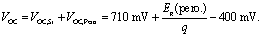
From the presented experimental results, we see that there is still some room for improvement when comparing with numerical studies, which predict efficiencies above 30%.26,28,35 In fabrication of the tandem devices, we were limited by some factors, namely our inability to spin-coat a high quality perovskite film below 500 nm thickness to enable more transmission into the bottom cell for current matching,40 and to freely tune the optical bandgap of the perovskite absorber while maintaining the low bandgap to VOC loss.41 To further reduce the discrepancy between simulation results and experimental realization of monolithic perovskite/silicon tandem solar cells, we establish an optical model, validate it with our experimental results and then use it to find guidelines for future experiments. For that, the wavelength-dependent complex refractive index (n,k) spectra needed to conduct the simulations were extracted from reflectance/transmittance (RT) or from spectroscopic ellipsometry using optical modelling, or from the literature for the perovskite absorber.42 The origin of the (n,k) spectra for all layers is stated in Table S1 (ESI†). To account for a higher bandgap of a Cs0.05(MA0.17FA0.83)Pb1.1(I0.83Br0.17)3 perovskite as compared to the usual CH3NH3I3, we perform a 20 nm blue shift of the perovskite (n,k) spectra used for simulations as experimentally justified in ref. 43 and 44. This has been shown to adequately present optical properties of a perovskite with a wider bandgap. The layer thicknesses in the stack were determined from SEM images as shown in Fig. 2, or from ellipsometry for SnO2 and IZO. All layers were considered to be coherent for the incident light as most of them are much thinner than the coherence length, except for silicon (250 μm) and the LM foil, which consists of a 100 μm thick polymer on top of 200 μm thick glass. We have also studied the effect of index matching liquid (IML) thickness on optical performance (see Fig. S6b, ESI†). Due to the IML having the same refractive index as glass and no absorption in the media, no difference was observed between implementing or not implementing the index matching liquid in our simulation.The matching between simulations and experiment is shown in Fig. 4. In both cases, without and with the LM foil, an excellent match is obtained. The perovskite bandgap shift matches well with experiment, and interference patterns are well aligned, validating the model and obtained (n,k) spectra. The thicknesses used in simulations for the best match and the corresponding integrated absorption spectra over the solar spectrum JSC_SIM are shown in Table S2 (ESI†). The JSC_SIM values match well with experimental JSC_EQE; the silicon photocurrent density differs by less than 4%, and the perovskite current density by less than 2%, while for reflection no difference is observed. We also simulate the possible improvement if our fabricated device would have been finished by evaporating a LiF layer as an AR coating instead of using the LM foil (see Fig. S6a, ESI†). For our not fully optically optimized device, the improvement with the LM foil is clear, especially in the silicon wavelength range.
 | ||
| Fig. 4 EQE and 1-R from experiment and simulation (a) without and (b) with the LM foil. The solid lines stand for experimental values and dashed lines represent simulations. Perovskite spectra are red, c-Si blue and 1-R black. | ||
Optimization of the different device designs
As already discussed in the Introduction, several optimizations of perovskite/SHJ tandem solar cells were already reported. Amongst the most important findings were: (i) using established contact materials, a p–i–n structure with an electron transport layer (ETL) on the front side is better due to less absorption losses in the charge selective layer on top of the perovskite (C60/PCBM as the ETL in the inverted architecture compared to spiro-OMeTAD as a hole transport layer in the regular architecture26,30); (ii) textures improve light management by in-coupling of light and light trapping;23,24 and (iii) very thick wide bandgap perovskites are needed for an optimal spectral division between the top and bottom cell.26,27 In the following, we aim to combine all of the findings to determine the realistically obtainable efficiency of the inverted monolithic perovskite/SHJ tandem with optimal bandgap, thickness, and textures at different interfaces.We start by optimizing the device (A) based on our experimental layer stack and (n,k) spectra as presented in ref. 25 and 26. We fixed the thicknesses of the layers in the bottom cell and allowed only the layers above the silicon substrate to vary in thickness. In addition, we also altered the perovskite bandgap in 20 nm steps between 0 and 80 nm (0 nm corresponds to the original perovskite CH3NH3PbI3 data with the absorption onset at around 795 nm – 1.56 eV42). For the efficiency estimations we assume a FF of 80% for all the device designs to allow a fair comparison on the optical changes due to textures. For this the optoelectrical quality of the perovskite film and adjacent contact layers should be the same, regardless of whether they are deposited on a planar or textured surface. The following equation was used for the VOC:
Proceeding from these results, we made the following assumptions for the optimization of the devices with textures: even with textures, the layer thicknesses of all the contact layers would stay mostly the same and thus their thicknesses are fixed for the simulations of the different texture positions, only the perovskite bandgap or its thickness would change. A higher bandgap is beneficial due to higher voltage potential, according to the abovementioned equation, if current matching can be realized. A thicker perovskite is beneficial because we can utilize a higher bandgap, however, we restricted the simulation to 1000 nm, as thicker layers are at the moment experimentally very hard to realize with high PCE.
Based on the validated assumptions discussed above, we performed optimizations of textured devices. With the validation, we reduce the investigated parameter space to the perovskite layer only. Hence, we could optimize devices with textured surfaces, which require computationally expensive ray-tracing approaches. We fixed the perovskite thickness to 1000 nm and tuned the bandgap in 5 nm steps until current matching was obtained. In simulations, we consider sharp transitions between layers that show bulk absorption. However, promising results with high PCEs were presented with graded heterojunctions48 and carbon monolayers from graphene49,50 that both may offer possible further improvements. We considered the device designs (A), (B), (C) and (D) as illustrated in Fig. 1. If the device has no LM foil, a planar AR coating (LiF) is considered. Table 2 shows the simulated optimal bandgap, extracted matched JSC_SIM, assumed FF and VOC for all the devices. As expected, the best case is device (D), followed by device (C) and device (B). According to our simulations, a both-side textured silicon tandem device (D) has the potential to reach a PCE of 32.5% for a perovskite thickness of 1000 nm and bandgap of 1.66 eV that would imply to have 1.26 V VOC from the perovskite top cell. Note that reducing the FF of device D to 77.5% due to potential lower perovskite film quality on the texture would mean that devices B, C and D would perform almost the same. Thus developing excellent perovskite film on the texture is necessary to enable the full potential of the double sided textured device D.
| Device design | E g opt. [eV] | J SC_SIM [mA cm−2] | V OC [V] | FF [%] | PCE [%] |
|---|---|---|---|---|---|
| Flat (A) | 1.69 | 19.07 | 2.00 | 80 | 30.5 |
| Back-side texture (B) | 1.65 | 20.01 | 1.96 | 80 | 31.4 |
| Back side texture + LM foil (C) | 1.66 | 19.97 | 1.97 | 80 | 31.5 |
| Both-side texture (D) | 1.66 | 20.56 | 1.97 | 80 | 32.5 |
Interestingly, the exact optimal bandgap to enable current matching highly depends on the device architecture and layers in the stack: recently, for the flat device (A) we found an optimal bandgap of 1.73 eV26 with close to 1.5 μm thickness. However, when utilizing less transparent C60 and IZO top layer (n,k) spectra derived from the measurements of the implemented films, a thickness above 2.4 μm is necessary to obtain current matching, see Table S3 (ESI†). Thus, the optimal bandgap for restricted maximal perovskite thickness of below 1 μm is 1.69 eV for flat tandems [device (A)] as presented in Table 2. When utilizing a back-side texture, the value even reduces to 1.65 eV as significantly more light is absorbed in the NIR regime, which is in agreement with previous work.31 This then has to be compensated for by a smaller bandgap of the top cell in order to achieve current matching, see Table 2. Such bandgaps are already very close to reported compositions with high efficiency and stability.45,46
The effect of the optimal top cell bandgap can be seen in Fig. 5a in which the simulated absorption spectra of all devices are shown for direct incident light as typically available in lab conditions. The most obvious effect is the benefit of using a back-side texture in the bottom cell. Despite having the same morphology on the front side, device (D) enables higher absorption values through the complete spectrum in both sub cells as compared to device (C). This is due to the different refractive index of the first layer (LM foil versus LiF) and different incident angles into the device; the device (C) still has a planar front-side in the top cell stack. Surprisingly, device (C) with a textured LM foil front side is only marginally better than device (B) with a planar AR coating (LiF) on the front. This is mostly due to the nc-SiOx:H layer, which dampens the interferences due to reflections from the silicon35 and reduces the improvement that the LM foil brings. Additionally, a flat front-side leads to a constructive interference at 1050 nm, which is beneficial for the long wavelength response.
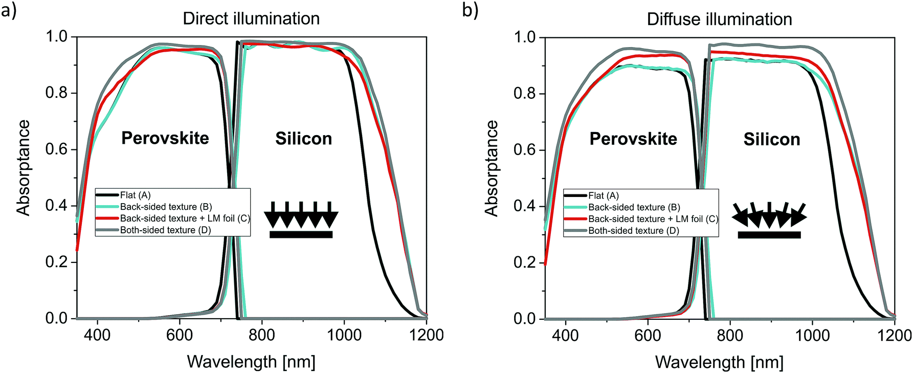 | ||
| Fig. 5 (a) Simulated absorption spectra for the device designs (A), (B), (C) and (D) and perovskite thickness 1000 nm where direct illumination is considered. (b) Simulated absorption spectra for the device designs (A), (B), (C) and (D) and perovskite thickness 1000 nm where diffuse illumination is considered. | ||
We also carried out simulations with perovskite thicknesses of 800 and 1200 nm, which serve as guidelines for a thickness already achievable in efficient devices and as a future possibility, respectively. The results and discussion can be found in the ESI† (Table S5 and Fig. S9). The most important finding is that increasing the perovskite thickness by 20%, only increases the PCE by 0.1% absolute. Thus, with a perovskite thickness of 1000 nm, we can already reach almost the maximal efficiency.
A detailed loss analysis, i.e. absorption spectra for all the layers in the stack, for the best performing device (D) with a 1000 nm thick perovskite is shown in Fig. S10 (ESI†) and the corresponding JSC_SIM values in Table S6 (ESI†). Assuming 100% carrier collection probability, from the 46.23 mA cm−2 available in the spectrum, 41.36 mA cm−2 is converted to charge carriers (20.56 mA cm−2 in the perovskite and 20.80 mA cm−2 in silicon), corresponding to an 89.5% yield of the available spectrum. This is very close to the best silicon single junction devices that yield a carrier generation current of 42.5 mA cm−2.51 The main losses are parasitic absorption in IZO and total reflection, both contributing to a 1.34 mA cm−2 loss. 0.6 mA cm−2 is absorbed by the C60 layer in the front contact and 0.35 mA cm−2 in the middle ITO layer. 1.18 mA cm−2 is absorbed in the back contact layers. Overall, very low parasitic losses are found for this device stack. By comparing the fabricated device and best simulated device (C) the biggest difference is in photocurrent utilization due to the non-optimized perovskite bandgap and thickness in the fabricated device (Fig. S10, S11 and Table S6, ESI†). The reflection is further reduced due to the both-side textured design, while IZO losses are lower due to a 40 nm thinner layer. Other losses are comparable. This confirms excellent optical performance of the monolithic perovskite/SHJ tandems utilizing contact layers from our experiment. To further reduce losses in the UV and blue region, the most viable options are developing a more transparent electron selective material with lower absorption than C60 (e.g. PCBM, however, its evaporation is not easy52) and using a less absorptive front TCO material such as IO:H.53,54 However, high temperature annealing of the IO:H at 150–200 °C to obtain optimal properties is an obstacle the perovskite film would have to survive. Additionally, the IO:H would also reduce free carrier reflection and parasitic free carrier absorption in the NIR. The losses in the back-contact could also be reduced by e.g. applying silicon nanoparticles as a back-side reflector.20
Until now, we have only considered direct, perpendicular illumination. However, to fully evaluate the effect of implementing textures in tandem cells, we need to move closer to outdoor conditions where diffuse light contributes a significant portion of the overall irradiation. To obtain absorption spectra under diffuse illumination, we repeated the simulations, but this time we assumed fully diffuse (Lambertian) incident illumination.14 The spectra with simulated diffuse illumination are shown in Fig. 5b. Compared to previous simulations under direct, perpendicular illumination, here a clear improvement with the LM foil can be observed in the full wavelength range of interest. This is a result of a more advantageous average incidence angle of diffuse light into device (C) as compared to device (B).
Energy yield analysis
Finally, we estimate the yearly energy yield (EY) for each of the designs. For simplicity, we assume non-encapsulated devices. This might underestimate the true potential of device C, as for our experimentally realized device C the LM foil stack (glass + textured LM foil) already resembles module encapsulation. The equations are explained in more detail in the ESI.† In short, for each hour in a year, we first simulate the absorption spectra of both sub cells, taking the position of the sun and the tilt of the module into account. Here we assumed a fixed tilt without tracking. Secondly, from the simulated absorption in the perovskite and silicon layers, we calculate the JSC_SIM of both cells, taking into account the spectrally dependent combined direct and diffuse illumination. Thirdly, we take the minimal JSC of both sub cells and the measured corresponding VOC and FF data to determine the generated energy during each hour of the year. Integrated over a year, the yearly EY can be obtained.28V OC and FF under different light intensities were measured on the fabricated tandem cell without the LM foil by altering the LED sun simulator intensity, starting at 100% AM1.5 (100 mW cm−2) and then sweeping from 10% AM1.5 to 120% AM1.5 in 10% steps. The results are shown in Fig. S12 (ESI†); in EY calculations they were then normalized at 100% light intensity to the predicted VOC estimated from the bandgap (see Table 2). As expected, the JSC increases linearly with increasing intensity and VOC logarithmically. The FF is slightly higher at lower intensities (lower current causes less series resistance induced power loss in the front contact), however, its value is relatively constant between 76 and 78%. The current for both 100% illumination measurements, first and eleventh, are the same, while VOC and FF improve slightly. This is not uncommon, a similar light soaking effect was recently reported albeit for a different hole transporting material – NiO.55 These results show that perovskite/SHJ devices can function well even at low irradiance levels.
We calculated the EY for three locations in the United States of America – Washington D.C., Golden and Phoenix. Their meteorological data is provided by NREL as a typical meteorological year (TMY).56 Averaged global horizontal irradiation (GHI) and direct normal irradiation (DNI) spectra over a year of each location are shown in Fig. S14 (ESI†), and the yearly incident irradiation for each location in Table S8 (ESI†). The locations were chosen in such a way that they receive different amounts of solar irradiance and the ratio between diffuse and direct illumination varies greatly. We investigated two tilts of the solar cells (modules): 30° and 90° facing south in the northern hemisphere. These tilts are relevant for rooftop or power plant, and building integrated photovoltaics (BIPV), respectively. The yearly EY for each of the discussed configurations for the two tilts are shown in Fig. 6 and all the corresponding values can be found in Table S7 (ESI†). The colored bars indicate the yearly EY in kW h m−2 and the dark blue bars the relative improvement compared to the flat device (A) without any texture. Phoenix, with the highest amount of solar irradiation, yields the highest amount of energy, almost 50% more than Washington D.C. for the 30° tilt. Interestingly, for the 90° tilt all the designs would produce more in Golden than in Phoenix. This is due to a higher part of diffuse illumination (see Table S8, ESI†), while the contribution from direct illumination is lower for the 90° tilt due to a greater direct incidence angle onto the device on the wall, contributing less than for the 30° tilt. Analyzing the yearly EY, a more pronounced improvement using LM foil compared to a planar AR coating is observed than in the basic simulation with only perpendicular illumination. This is even more apparent for the BIPV application (90°) where with the LM foil more than 4.5% extra energy can be gained. Overall, device (D) is still the most promising configuration with ∼9.5% and ∼12% relative improvement to the fully flat device (A), for the 30° and 90° tilt, respectively. Assuming again that the FF of device D is 77.5 due to slightly poorer perovskite film or contact quality on the texture, 15 to 20 kW h m−2 would be lost. This makes the relative difference between devices C and D less than 1%. In addition the glass encapsulation scheme as typically used in modules is already partially already included in device C, thus the herein calculated benefit of device D is even less pronounced. Nevertheless, these results show that strong improvements in EY are expected for textured front-sides, even when just applying a textured LM foil on top of a planar wafer.
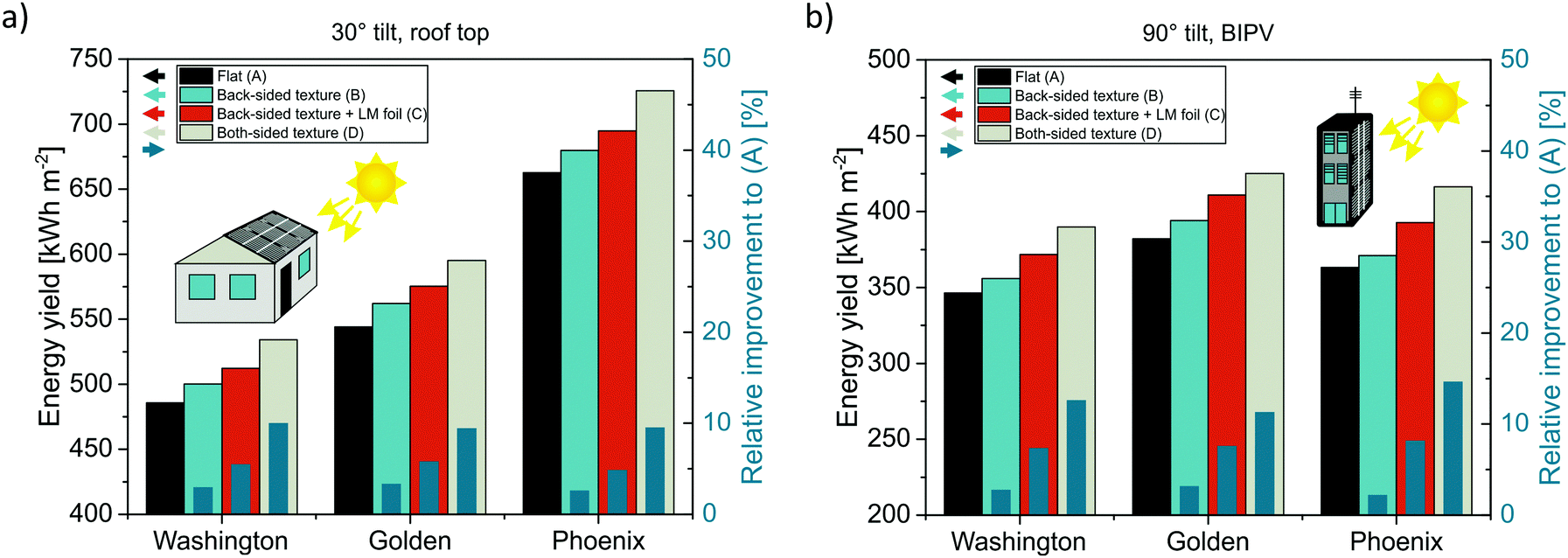 | ||
| Fig. 6 Simulated yearly energy yield for different device designs (A), (B), (C), and (D) for (a) 30° and (b) 90° solar cell orientation/inclination and relative improvement to design (A) (right y-axis). Three different locations, Washington DC, Golden and Phoenix are compared. | ||
Conclusion
In conclusion, we analyzed the effect of different positions of interface textures in monolithic perovskite/silicon-heterojunction tandem devices. We fabricated a highly efficient flat front-side/textured back-side tandem device. Using a textured light management (LM) foil on top, we improved the power conversion efficiency (PCE) from 23.4 to 25.5%. This is among the highest reported values for 2-terminal perovskite/silicon tandem solar cells. The high efficiency was enabled by excellent light management and low parasitic absorption losses. By applying the LM foil, our experimentally realized tandem device already resembles final module integration. We further developed an optical model, using experimental results on the refractive indices of all films in the cell stack, which showed excellent agreement between experimental and simulated spectra. We then used the validated model to predict the realistically obtainable efficiencies of four different textured tandem devices, and the optimal bandgap and thickness of the perovskite absorber. For the best performing design, the tandem solar cell with the silicon wafer textured on both sides, we determined the optimal bandgap to be 1.66 eV and a PCE potential of 32.5% based on a top cell VOC of 1.26 V. To reduce the optical losses, which mostly occur due to reflection, and absorption in the front TCO and in the back contact, thicknesses of all contact layers should be minimized. The loss comparison between the fabricated device and the best simulated case shows that the main difference is in reflection and in the parasitic absorption in the front TCO contact, despite its excellent transparency. Thus, even more conductive and transparent TCOs are needed. By extending our model to calculate the performance under diffuse illumination, we estimated the yearly energy yield for three different geographical locations and with two different tilts of the device, 30° and 90°. For the 90° tilt, the diffuse light plays a much larger role than direct illumination as compared to the 30° tilt. Additionally, when comparing the performance of the devices over a year, we observed that front-side textured devices significantly outperform front-side planar devices. Thus, having front-side textures is beneficial for a high energy yield, especially when building-integrated photovoltaics is considered. The results obtained in this study should serve as a guideline towards highly efficient monolithic perovskite/silicon-heterojunction tandem devices in both lab and outdoor applications.Methods
Perovskite materials
Anhydrous DMSO (dimethyl sulfoxide), DMF (dimethylformamide), and toluene were purchased from Sigma Aldrich. PTAA (poly[bis(4-phenyl)(2,5,6-trimentlyphenyl)amine]) and C60 (purity = 99.9%) were purchased from Sigma Aldrich. FAI (formamidinium iodide) and MABr (methylammonium bromide) were purchased from Dyenamo. PbI2 and PbBr2 were bought from TCI. CsI was purchased from abcr GmbH.Perovskite solar cell preparation
The fabricated perovskite sub cell has an inverted (p–i–n) planar structure and a layer configuration of Si substrate/ITO/PTAA/Perovskite/C60/SnO2/IZO, where IZO is zinc doped indium oxide. The silicon substrates were briefly ultrasonicated in isopropanol before use. All the spin-coating layer deposition steps were conducted in a nitrogen atmosphe.re The hole transport material PTAA (2 mg ml−1 in toluene) was deposited using spin-coating (4000 rpm for 30 s) and annealed for 10 min at 100 °C. The perovskite was prepared following the typical “triple cation” process.38,57 In short, 1.5 M nominal PbI2 and PbBr2 in DMF:DMSO = 4:1 volume were first prepared as stock solutions and then added to FAI and MABr with 10% PbX2 excess, respectively (X = I or Br). The so obtained FAPbI3 and MAPbBr3 were then mixed in 5:1 volume ratio to obtain the “double cation” perovskite. Finally, 5% volume of 1.5 M nominal CsI in DMSO was added to form the “triple cation” perovskite. 100 μl of perovskite solution was then spread on the substrate and spun using one step spin-coating process (4000 rpm for 35 s). 25 s after the start of a spinning, 400 μl ethyl acetate anti-solvent drop was utilized. The films were annealed at 100 °C for 1 h. Afterwards, 15 nm C60 was thermally evaporated at a rate of 0.15 A s−1 at 400 °C. 20 nm SnO2 were prepared by thermal ALD in an Arradiance GEMStar reactor. Tetrakis(dimethylamino)tin(IV) (TDMASn) was used as the Sn precursor and was held at 60 °C in a stainless steel container. Water was used as oxidant, and was delivered from a stainless steel container without intentional heating. IZO was sputtered in a Roth&Rau MicroSys 200 PVD. The 2 inch ceramic target consisted of 90 wt% In2O3 and 10 wt% ZnO. At a RF-power of 70 W the cells oscillated under the target to have a uniform deposition. In order to achieve transparent films, the plasma was a mix of argon and 0.2 vol% oxygen. With these settings, the deposited layer has a mobility of 44.7 cm2 V−1 s−1 and a carrier concentration of 3.5 × 1020 cm−3, as characterized previously on a witness sample on glass. Finally, a 180 nm thick Ag metal frame was evaporated as a top contact, defining the active area of 0.81 cm2. For the single-junction solar cell, the back contact consisted of 23 nm C60, 8 nm BCP and 100 nm Ag.
Silicon solar cell preparation
The silicon heterojunction (SHJ)-bottom cell was fabricated on a 260 μm thick polished FZ 〈100〉 n-type crystalline silicon (c-Si) wafer in a rear junction configuration. The front surface of the wafer was left polished in order to facilitate the perovskite top cell deposition, while the rear surface of the wafer was chemically textured to obtain random pyramids with 〈111〉 facets in order to improve the optical response of the bottom cell in the NIR region. After a final RCA clean and a 3 minute HF dip (1% dilution in water) to strip the native SiO2 of the surface, a 5 nm thick, intrinsic (i) amorphous silicon (a-Si) layer was grown on both sides of the c-Si wafer in order to passivate the c-Si surface. On the textured rear-side, a 5 nm thick, p-doped a-Si layer was deposited. On the polished front-side, a 95 nm thick, n-doped nanocrystalline silicon oxide layer (nc-SiOx:H) with a refractive index, n, of 2.7 at 650 nm was used as a front surface field (FSF) of the SHJ bottom cell and intermediate layer between the top and the bottom cells. All the a- and nc-Si layers were deposited with an Applied Materials (AKT1600) plasma enhanced chemical vapor deposition (PECVD) tool. In order to contact the bottom cell a full area ZnO:Al/Ag layer stack was deposited on the textured back-side and a 20 nm thick ITO layer was deposited on the polished front-side on top of the nc-SiOx:H interlayer; both depositions were DC-sputtered in an in-line sputtering tool from Leybold Optics. The TCO and TCO + metal contact layers were sputtered using shadow masks with an opening of 1 cm2.Device characterization
The current density–voltage (JV) measurements were performed under standard test conditions (25 °C, dual light source sun simulator, class AAA), adjusted with a filtered and non-filtered calibrated silicon reference cell (Fraunhofer ISE). The scan rate was 0.125 V s−1 with a voltage step of 10 mV. Masks with different areas were used; the small mask had the area of 0.77 cm2, which is only slightly smaller than the active area of 0.81 cm2; the larger mask had the area of 1 cm2, which is the same as the contact layers (IZO, ITO, AZO) of the device stack, excluding the front silver frame. The light intensity dependent JV measurements were performed on a tandem device without the LM foil under standard test conditions (25 °C, LED sun simulator, Wavelabs, class AAA), adjusted with a calibrated silicon reference cell (Fraunhofer ISE). The light intensity was then swept from 10% AM1.5 to 120% AM1.5 in 10% steps. The external quantum efficiency (EQE) was measured as a function of wavelength from 300 to 1200 nm with a step of 10 nm using a home built small spot EQE system. The beam size is 2 × 5 mm2, thus smaller than the active area. When measuring the perovskite top cell blue and red bias light were applied along with a 0.6 V bias voltage. When measuring the silicon bottom cell blue bias light was applied. Reflection was measured as a function of wavelength from 300 to 1200 nm with a step of 5 nm using an integrating sphere with a Perkin Elmer Lambda – 1050 UV/vis/NIR spectrophotometer, calibrated with a white Spectralon.Spectroscopic ellipsometry
The optical constants of SnO2 and IZO over a wavelength range of 240–2400 nm were determined by spectroscopic ellipsometry. Measurements were performed using a Sentech ellipsometer, and Tauc–Lorentz oscillators were used to model the dielectric function of the SnO2.Optical simulations
Flat device optimization was done using GenPro4.58 We globally maximized the minimum of the top and bottom cell current densities with the “GlobalSearch” algorithm that is implemented in Matlab (The MathWorks, Inc., Natick, Massachusetts, United States). For the optimization we used the same layer stack and (n,k) spectra as in the Validation section. We fixed the layer thicknesses of the bottom sub cell and allowed only the layers above the silicon substrate to vary in thickness. The thickness constraints were set to experimentally relevant values. In addition, we also altered the perovskite bandgap in 20 nm steps between 0 and 80 nm (the 0 nm step corresponds to data for a CH3NH3PbI3 perovskite with the absorption onset at around 800 nm – 1.56 eV42).The textured device optimization was done using CROWM.14,15 The simulator is based on combined ray and wave optics models that enable simultaneous simulations of all segments of the device; the thick textured LM foil, the silicon wafer (incoherent light propagation assumed in both cases), and the thin-film solar cell stack(s) (coherent light propagation assumed). As the input parameters, realistic thicknesses and experimentally determined refractive indices of the materials were employed. The imaginary part of the refractive index of the perovskite absorber was wavelength-shifted to obtain the different bandgaps. The main outputs of the simulator are total reflectance, transmittance and absorptance in each layer. Their solar-spectrum wavelength integration equals the generated JSC or the equivalent JSC loss in each individual layer. The simulations were carried out in the wavelength range from 350 to 1200 nm which is a sufficiently broad range for the analyzed tandem solar cells. To include a realistic texture in the simulations, the texture profile of the random pyramids was obtained using atomic force microscopy (AFM) and imported directly into the simulator.
Author contributions
M. J., E. K., and A. A. developed and optimized the perovskite process. E. K. fabricated the tandem device, M. J. fabricated the LM foil. M. J. and E. K. performed the measurements and optimized the top contact. A. B. M. V., L. K. and B. S. developed the silicon-heterojunction project and fabricated silicon substrates. B. M. optimized the SnO2 process and performed and analysed spectroscopic ellipsometry measurements. M. J., B. L., K. J. and J. K. performed the optical simulations. M. J. and S. A. wrote the manuscript. All authors participated in proofreading and correcting it. B. R., R. S., M. T., B. S. and S. A. supervised the project.Conflicts of interest
There are no conflicts to declare.Acknowledgements
The authors thank Carola Klimm, Institute for Silicon Photovoltaics, for performing SEM images, Florian Ruske, Institute for Silicon Photovoltaics, for help with spectroscopic ellipsometry, and Kerstin Jacob, Institute for Silicon Photovoltaics, and Tobias Henschel and Katja Mayer-Stillrich, PVcomB, for help in the bottom cell processing. The authors acknowledge the funding by the German Federal Ministry of Education and Research (BMBF) via program “Materialforschung fuer die Energiewende” (grant no. 03SF0540), the support provided by the German Federal Ministry for Economic Affairs and Energy (BMWi) through the “PersiST” project (Grant No. 0324037C), bilateral project BI-DE/2017-2019/004 (German Academic Exchange Service (DAAD) and Slovene Research Agency (ARRS)) and research program P2-0197 (ARRS).References
- S. Albrecht and B. Rech, Perovskite solar cells: On top of commercial photovoltaics, Nat. Energy, 2017, 2(1), 16196 CrossRef.
- J. Werner, B. Niesen and C. Ballif, Perovskite/Silicon Tandem Solar Cells: Marriage of Convenience or True Love Story? – An Overview, Adv. Mater. Interfaces, 2017, 5(1), 1700731 CrossRef.
- T. Leijtens, K. A. Bush, R. Prasanna and M. D. McGehee, Opportunities and challenges for tandem solar cells using metal halide perovskite semiconductors, Nat. Energy, 2018, 1 Search PubMed.
- M. A. Green, Y. Hishikawa, E. D. Dunlop, D. H. Levi, J. Hohl-Ebinger and A. W. Y. Ho-Baillie, Solar cell efficiency tables (version 52), Prog. Photovoltaics, 2018, 26(7), 427–436 Search PubMed.
- F. Sahli, et al., Fully textured monolithic perovskite/silicon tandem solar cells with 25.2% power conversion efficiency, Nat. Mater., 2018, 1 Search PubMed.
- T. Duong, et al., Rubidium Multication Perovskite with Optimized Bandgap for Perovskite-Silicon Tandem with over 26% Efficiency, Adv. Energy Mater., 2017, 7(14), 1700228 CrossRef.
- C. O. R. Quiroz, et al., Balancing electrical and optical losses for efficient 4-terminal Si–perovskite solar cells with solution processed percolation electrodes, J. Mater. Chem. A, 2018, 6(8), 3583–3592 RSC.
- I. Zubel and I. Barycka, Silicon anisotropic etching in alkaline solutions I. The geometric description of figures developed under etching Si(100) in various solutions, Sens. Actuators, A, 1998, 70(3), 250–259 CrossRef CAS.
- C. Battaglia, A. Cuevas and S. D. Wolf, High-efficiency crystalline silicon solar cells: status and perspectives, Energy Environ. Sci., 2016, 9(5), 1552–1576 RSC.
- D. Chen, et al., Nanophotonic light management for perovskite–silicon tandem solar cells, J. Photonics Energy, 2018, 8(2), 022601 Search PubMed.
- C. Momblona, et al., Efficient vacuum deposited p-i-n and n-i-p perovskite solar cells employing doped charge transport layers, Energy Environ. Sci., 2016, 9(11), 3456–3463 RSC.
- J. Werner, et al., Efficient Monolithic Perovskite/Silicon Tandem Solar Cell with Cell Area >1 cm2, J. Phys. Chem. Lett., 2015, 161–166 Search PubMed.
- M. Jošt, et al., Efficient Light Management by Textured Nanoimprinted Layers for Perovskite Solar Cells, ACS Photonics, 2017, 4(5), 1232–1239 CrossRef.
- B. Lipovšek, J. Krč and M. Topič, Microtextured Light-Management Foils and Their Optimization for Planar Organic and Perovskite Solar Cells, IEEE J. Photovolt., 2018, 8(3), 783–792 Search PubMed.
- B. Lipovšek, et al., Detailed optical modelling and light-management of thin-film organic solar cells with consideration of small-area effects, Opt. Express, 2017, 25(4), A176–A190 CrossRef PubMed.
- C. Trompoukis, et al., Photonic nanostructures for advanced light trapping in thin crystalline silicon solar cells, Phys. Status Solidi A, 2015, 212(1), 140–155 CrossRef CAS.
- J. P. Mailoa, et al., A 2-terminal perovskite/silicon multijunction solar cell enabled by a silicon tunnel junction, Appl. Phys. Lett., 2015, 106(12), 121105 CrossRef.
- S. Albrecht, et al., Monolithic perovskite/silicon-heterojunction tandem solar cells processed at low temperature, Energy Environ. Sci., 2016, 9(1), 81–88 RSC.
- J. Werner, et al., Efficient Near-Infrared-Transparent Perovskite Solar Cells Enabling Direct Comparison of 4-Terminal and Monolithic Perovskite/Silicon Tandem Cells, ACS Energy Lett., 2016, 1(2), 474–480 CrossRef CAS.
- K. A. Bush, et al., 23.6%-efficient monolithic perovskite/silicon tandem solar cells with improved stability, Nat. Energy, 2017, 2(4), 17009 CrossRef CAS.
- L. Mazzarella, et al., submitted.
- S. Manzoor, et al., Improved light management in planar silicon and perovskite solar cells using PDMS scattering layer, Sol. Energy Mater. Sol. Cells, 2017, 173, 59–65 CrossRef CAS.
- M. Filipič, et al., CH3NH3PbI3 perovskite/silicon tandem solar cells: characterization based optical simulations, Opt. Express, 2015, 23(7), A263 CrossRef PubMed.
- R. Santbergen, et al., Minimizing optical losses in monolithic perovskite/c-Si tandem solar cells with a flat top cell, Opt. Express, 2016, 24(18), A1288–A1299 CrossRef CAS PubMed.
- S. Albrecht, et al., Towards optical optimization of planar monolithic perovskite/silicon-heterojunction tandem solar cells, J. Opt., 2016, 18(6), 064012 CrossRef.
- K. Jäger, L. Korte, B. Rech and S. Albrecht, Numerical optical optimization of monolithic planar perovskite-silicon tandem solar cells with regular and inverted device architectures, Opt. Express, 2017, 25(12), A473–A482 CrossRef PubMed.
- M. T. Hörantner, et al., The Potential of Multijunction Perovskite Solar Cells, ACS Energy Lett., 2017, 2(10), 2506–2513 CrossRef.
- M. T. Hörantner and H. J. Snaith, Predicting and optimising the energy yield of perovskite-on-silicon tandem solar cells under real world conditions, Energy Environ. Sci., 2017, 10(9), 1983–1993 RSC.
- S. Rühle, The detailed balance limit of perovskite/silicon and perovskite/CdTe tandem solar cells, Phys. Status Solidi A, 2017, 214(5), 1600955 CrossRef.
- S. Altazin, L. Stepanova, J. Werner, B. Niesen, C. Ballif and B. Ruhstaller, Design of perovskite/crystalline-silicon monolithic tandem solar cells, Opt. Express, 2018, 26(10), A579–A590 CrossRef CAS PubMed.
- K. Jäger, et al., Numerical Optical Optimization of Perovskite-Silicon Tandem Solar Cells, 33rd Eur. Photovolt. Sol. Energy Conf. Exhib., 2017, pp. 1057–1060.
- B. Kirn, K. Brecl and M. Topic, A new PV module performance model based on separation of diffuse and direct light, Sol. Energy, 2015, 113, 212–220 CrossRef.
- J. Lehr, M. Langenhorst, R. Schmager, S. Kirner, U. Lemmer, B. S. Richards, C. Case and U. W. Paetzold, Sustainable Energy Fuels, 2018 10.1039/C8SE00465J.
- M. H. Futscher and B. Ehrler, Modeling the Performance Limitations and Prospects of Perovskite/Si Tandem Solar Cells under Realistic Operating Conditions, ACS Energy Lett., 2017, 2(9), 2089–2095 CrossRef CAS PubMed.
- L. Mazzarella, et al., Infrared photocurrent management in monolithic perovskite/silicon heterojunction tandem solar cells by using a nanocrystalline silicon oxide interlayer, Opt. Express, 2018, 26(10), A487–A497 CrossRef PubMed.
- M. Stolterfoht, et al., Approaching the Fill Factor Shockley–Queisser Limit in Stable, Dopant-Free Triple Cation Perovskite Solar Cells, Energy Environ. Sci., 2017, 10(6), 1530–1539 RSC.
- C. M. Wolff, F. Zu, A. Paulke, L. P. Toro, N. Koch and D. Neher, Reduced Interface-Mediated Recombination for High Open-Circuit Voltages in CH3NH3PbI3 Solar Cells, Adv. Mater., 2017, 29(28), 1700159 CrossRef PubMed.
- M. Saliba, T. Matsui, J.-Y. Seo, K. Domanski, J.-P. Correa-Baena, M. K. Nazeeruddin, S. M. Zakeeruddin, W. Tress, A. Abate, A. Hagfeldt and M. Grätzel, Cesium-containing triple cation perovskite solar cells: improved stability, reproducibility and high efficiency, Energy Environ. Sci., 2016, 9, 1989–1997 RSC.
- W. E. McMahon, et al., Fill factor as a probe of current-matching for GaInP2/GaAs tandem cells in a concentrator system during outdoor operation, Prog. Photovoltaics, 2008, 16(3), 213–224 Search PubMed.
- J. Werner, et al., Complex Refractive Indices of Cesium–Formamidinium-Based Mixed-Halide Perovskites with Optical Band Gaps from 1.5 to 1.8 eV, ACS Energy Lett., 2018, 3(3), 742–747 CrossRef CAS.
- E. L. Unger, L. Kegelmann, K. Suchan, D. Sörell, L. Korte and S. Albrecht, Roadmap and roadblocks for the band gap tunability of metal halide perovskites, J. Mater. Chem. A, 2017, 5(23), 11401–11409 RSC.
- P. Löper, et al., Complex Refractive Index Spectra of CH3NH3PbI3 Perovskite Thin Films Determined by Spectroscopic Ellipsometry and Spectrophotometry, J. Phys. Chem. Lett., 2015, 6(1), 66–71 CrossRef PubMed.
- D. P. McMeekin, et al., A mixed-cation lead mixed-halide perovskite absorber for tandem solar cells, Science, 2016, 351(6269), 151–155 CrossRef CAS PubMed.
- A. Tejada, S. Braunger, L. Korte, S. Albrecht, B. Rech and J. A. Guerra, Optical characterization and bandgap engineering of flat and wrinkle-textured FA0.83Cs0.17Pb(I1−xBrx)3 perovskite thin films, J. Appl. Phys., 2018, 123(17), 175302 CrossRef.
- M. Saliba, et al., Incorporation of rubidium cations into perovskite solar cells improves photovoltaic performance, Science, 2016, aah5557 Search PubMed.
- D. Luo, et al., Enhanced photovoltage for inverted planar heterojunction perovskite solar cells, Science, 2018, 360(6396), 1442–1446 CrossRef CAS PubMed.
- Z. Chen, et al., Thin single crystal perovskite solar cells to harvest below-bandgap light absorption, Nat. Commun., 2017, 8(1), 1890 CrossRef PubMed.
- Y. Wu, et al., Perovskite solar cells with 18.21% efficiency and area over 1 cm2 fabricated by heterojunction engineering, Nat. Energy, 2016, 1(11), 16148 CrossRef CAS.
- F. Lang, et al., Perovskite Solar Cells with Large-Area CVD-Graphene for Tandem Solar Cells, J. Phys. Chem. Lett., 2015, 6(14), 2745–2750 CrossRef CAS PubMed.
- E. Bi, et al., Diffusion engineering of ions and charge carriers for stable efficient perovskite solar cells, Nat. Commun., 2017, 8, 15330 CrossRef CAS PubMed.
- A. Richter, J. Benick, F. Feldmann, A. Fell, M. Hermle and S. W. Glunz, n-Type Si solar cells with passivating electron contact: Identifying sources for efficiency limitations by wafer thickness and resistivity variation, Sol. Energy Mater. Sol. Cells, 2017, 173, 96–105 CrossRef CAS.
- B. W. Larson, et al., Thermal [6,6] → [6,6] Isomerization and Decomposition of PCBM (Phenyl-C61-butyric Acid Methyl Ester), Chem. Mater., 2014, 26(7), 2361–2367 CrossRef CAS.
- B. Macco, Y. Wu, D. Vanhemel and W. M. M. Kessels, High mobility In2O3:H transparent conductive oxides prepared by atomic layer deposition and solid phase crystallization, Phys. Status Solidi RRL, 2014, 8(12), 987–990 CrossRef CAS.
- B. Macco, H. C. M. Knoops and W. M. M. Kessels, Electron Scattering and Doping Mechanisms in Solid-Phase-Crystallized In2O3:H Prepared by Atomic Layer Deposition, ACS Appl. Mater. Interfaces, 2015, 7(30), 16723–16729 CrossRef CAS PubMed.
- H. Tsai, et al., Light-induced lattice expansion leads to high-efficiency perovskite solar cells, Science, 2018, 360(6384), 67–70 CrossRef CAS PubMed.
- NSRDB Viewer|National Solar Radiation Database (NSRDB), [online], available: https://nsrdb.nrel.gov/nsrdb-viewer, [accessed: 07-Jul-2018].
- M. Saliba, et al., How to Make over 20% Efficient Perovskite Solar Cells in Regular (n–i–p) and Inverted (p–i–n) Architectures, Chem. Mater., 2018, 30(13), 4193–4201 CrossRef CAS.
- R. Santbergen, T. Meguro, T. Suezaki, G. Koizumi, K. Yamamoto and M. Zeman, GenPro4 Optical Model for Solar Cell Simulation and Its Application to Multijunction Solar Cells, IEEE J. Photovolt., 2017, 7(3), 919–926 Search PubMed.
Footnote |
| † Electronic supplementary information (ESI) available. See DOI: 10.1039/c8ee02469c |
| This journal is © The Royal Society of Chemistry 2018 |