
 Open Access Article
 This Open Access Article is licensed under a
 Creative Commons Attribution 3.0 Unported Licence
Tin(IV) chalcogenoether complexes as single source precursors for the chemical vapour deposition of SnE2 and SnE (E = S, Se) thin films†
Chitra
Gurnani
a,
Samantha L.
Hawken
b,
Andrew L.
Hector
 b,
Ruomeng
Huang
c,
Marek
Jura
d,
William
Levason
b,
James
Perkins
b,
Gillian
Reid
*b and
Gavin B. G.
Stenning
d
b,
Ruomeng
Huang
c,
Marek
Jura
d,
William
Levason
b,
James
Perkins
b,
Gillian
Reid
*b and
Gavin B. G.
Stenning
d
aSchool of Natural Sciences, Mahindra Ecole Centrale, Hyderabad, India
bChemistry, University of Southampton, Southampton SO17 1BJ, UK. E-mail: G.Reid@soton.ac.uk
cElectronic and Computer Science, University of Southampton, Southampton SO17 1BJ, UK
dISIS Neutron and Muon Source, Rutherford Appleton Laboratory, Harwell Science and Innovation Campus, Didcot, OX11 0QX, UK
First published on 2nd February 2018
Abstract
The molecular Sn(IV) complexes, [SnCl4{nBuS(CH2)3SnBu}] (2), [SnCl4(nBu2S)2] (3) and [SnCl4(nBu2Se)2] (4) have been prepared in good yield from reaction of SnCl4 with the appropriate chalcogenoether ligand in anhydrous hexane and, together with the known [SnCl4{nBuSe(CH2)3SenBu}] (1), employed as single source precursors for the low pressure chemical vapour deposition of the corresponding tin dichalcogenide thin films. At elevated temperatures the bidentate ligand precursors, (1) and (2), also form the tin monochalcogenides, SnSe and SnS, respectively. In contrast, (3) gave a mixture of phases, SnS2, Sn2S3 and SnS and (4) gave SnSe2 only. The morphologies, elemental compositions and crystal structures of the resulting films have been determined by scanning electron microscopy, energy dispersive X-ray spectroscopy, grazing incidence X-ray diffraction and Raman spectroscopy. Van der Pauw measurements on the SnS2, SnS and SnSe2 films confirm their resistivities to be 2.9(9), 266(3) and 4.4(3) Ω cm, respectively.
Introduction
Tin chalcogenides (SnEx) (E = S, Se; x = 1, 2) are layered semiconducting materials that are becoming widely acknowledged as important for a wide variety of electronic applications; specifically optoelectronics,1–5 thermoelectrics6,7 and phase change devices.8,9 SnS2 also shows potential for use in photodetectors, with a high external quantum efficiency of 3.2 × 10⁵%;1 high performance sodium storage, with a high reversible capacity reported of 576 mA h g−1;10 and phototransistors with a high on/off ratio reported of >106.2 SnS, on the other hand, has a very low thermal conductivity ∼0.29 W mK−1 and a reported ZT value of 0.41,7 which are of particular interest for thermoelectric devices, whilst ZT values as high as 2.6 have been claimed for single crystals of SnSe.7 SnSe2 has attracted interest as a potentially effective phase change material for data storage applications. For this application fast recrystallisation times are key and SnSe2, with a recrystallisation time of 20 ns,9 is a promising material in this field.Tin chalcogenide thin films can be produced by a variety of methods. Using atmospheric pressure chemical vapour deposition and a dual source precursor approach, SnCl4 with either H2S or Et2Se can produce SnS2 or SnS,11,12 and SnSe2 or SnSe,13 respectively, depending on the conditions employed. A single source precursor approach, in which the metal and chalcogen are incorporated into one molecular compound, can lead to easier to handle precursors (since they are coordinatively saturated), potentially easier control of stoichiometry and, in some cases, the ability to deposit the binary material selectively onto specific regions of a patterned substrate on the micro-14 or nano-scale.15 While this substrate selectivity is rather atypical of CVD, it can be highly advantageous for certain applications.
In previous work, SnS and SnS2 have been produced from the tin(IV) thiolate complex, [Sn(SCH2CH2S)2], using aerosol assisted chemical vapour deposition in the presence of H2S gas,16 or using alkyl tin dithiocarbamates17 and SnS nanosheets by liquid exfoliation.18 Single source precursor approaches to tin sulfide and selenide thin films by us have used the thio- and seleno-ether complexes, [SnCl4{o-C6H4(CH2EMe)2}] (E = S, Se)19 to produce SnS2 and small amounts of SnS and SnSe, or; [SnCl4(SeEt2)2]19 and [SnCl4{nBuSe(CH2)xSenBu}] (x = 2, 3)20 to form SnSe2. Within the chalcogenoether- and chalcogenolate-based precursors, terminal butyl substituents have been shown to be well-suited for the growth of high quality binary chalcogenide thin films. This is attributed to their clean, low energy β-hydride elimination pathway.
Here we report the synthesis, characterisation and evaluation of three novel single source precursors, [SnCl4{nBuS(CH2)3SnBu}] (2) and [SnCl4(nBu2E)2] (E = S, (3); E = Se, (4)), and their use for the low pressure chemical vapour deposition (LPCVD) of SnS2 and SnSe2 thin films, as well as variation of the deposition conditions to produce SnSe and SnS films. High temperature LPCVD using [SnCl4{nBuSe(CH2)3SenBu}], (1), is also explored as a route to SnSe films.
Energy dispersive X-ray (EDX), scanning electron microscopy (SEM), Raman spectroscopy and grazing incidence X-ray diffraction (XRD) data on the resulting films are presented, together with resistivities determined by van der Pauw measurements.
Experimental
Precursor preparation and characterisation
All reactions were conducted using Schlenk, vacuum line and glove box techniques under a dry nitrogen atmosphere. The reagents were stored and manipulated using a glove box. Hexane was dried by distillation over sodium wire. SnCl4, nBuLi (1.6 mol dm−3 in diethyl ether) and nBu2S were obtained from Sigma-Aldrich. nBu2S was dried over sieves, SnCl4 and nBuLi were used as received. nBu2Se,21nBuSe(CH2)3SenBu20 and [SnCl4{nBuSe(CH2)3SenBu}]20 (1) were prepared according to the literature methods. IR spectra were recorded as Nujol mulls between CsI plates using a PerkinElmer Spectrum 100 instrument. 1H and 13C{1H} NMR spectra were recorded from solutions in CDCl3 or CD2Cl2 on a Bruker AV400 spectrometer, 77Se{1H} and 119Sn NMR spectra on a Bruker AV400-II spectrometer and referenced to external neat SeMe2 and SnMe4 respectively. A small amount of [Cr(acac)3] was added as a relaxation agent to the samples for 119Sn NMR measurements. Microanalytical results were obtained from Medac Ltd.n BuS(CH 2 ) 3 S n Bu: was obtained by dissolving HS(CH2)3SH (6.05 g, 56 mmol) in anhydrous EtOH (60 mL) with addition of elemental sodium (2.8 g, 112 mmol) cut into small pieces. After dissolution of the sodium, the reaction mixture was refluxed for 1 h, cooled to ambient temperature and nBuBr (15.34 g, 12.03 mL, 112 mmol) was added slowly. The reaction mixture was then refluxed for 1 h, forming a white solid. After cooling, saturated aqueous NaCl and NaHCO3 solutions were added. After filtering, the product was extracted from the aqueous filtrate with Et2O (4 × 50 mL), dried overnight (Na2SO4) and, after removal of the drying agent, the solvent was removed in vacuo, leaving a colourless oil. Yield: 6.0 g, 48%. 1H NMR (CDCl3, 298 K) δ/ppm: 0.92 (t, [6H], CH3), 1.41 (m, [4H], –CH2CH3), 1.57 (m, [4H], –SCH2CH2CH2CH3), 1.86 (m, [2H], –SCH2CH2CH2S–), 2.52 (t, [4H], SCH2–), 2.62 (t, [4H], SCH2–). 13C{1H} NMR (CDCl3, 298 K) δ/ppm 13.65 (CH3), 21.98, 29.43, 30.96, 31.74, 31.81 (all CH2).
LPCVD onto PVD SiO2 substrates
Physical vapour deposited (PVD) SiO2 on Si substrates were prepared as described previously.20 In a typical LPCVD experiment the reagent (70–80 mg) and PVD SiO2 substrates were loaded into a closed end silica tube in a glove box (precursor in bulb at closed end and followed by four substrate tiles (each 20 × 8 × 1 mm) positioned adjacently along the tube). The tube was placed horizontally in the furnace such that the precursor was outside of the heated zone. The tube was evacuated to 0.02 mmHg. The furnace was then heated to the desired temperature and the temperature was allowed to stabilise. The tube was then repositioned, if necessary, to move the precursor closer to the heated zone to a point where sublimation could be observed. At this point the position of the tube was maintained until the deposition was complete (i.e. the precursor was completely sublimed). This typically took 1–3 hours. Once complete, the tube was allowed to cool to room temperature and transferred to the glove box where the substrates were removed and stored under N2 before characterization.The LPCVD experiments produced black or silver films. Precursors 1 and 4 typically gave SnSe2 at all temperatures up to 1023 K. Precursor 2 gave SnS2 at all temperatures and 3 gave SnS2 at low temperatures and Sn2S3 at higher temperatures. These results were confirmed to be reproducible. It was noted that on the occasions when precursors 1 and 2 travelled further into the heated zone, SnSe and SnS films, respectively, were obtained.
Thin film characterisation
X-ray diffraction (XRD) patterns were collected in grazing incidence on a Rigaku SmartLab system, using CuKα X-rays, a 2θ scan range of 10–80° and an ω-offset of 0.7 or 1°. The crystalline phase of the films was determined by matching to a literature XRD pattern22 and lattice parameters calculated by further optimisation of the fit using PDXL.23 Scanning electron microscopy (SEM) images and energy dispersive X-ray (EDX) measurements were obtained using a JEOL JSM 6500 F Field Emission Scanning Electron Microscope with an Oxford INCA x-sight 7418 EDX probe. An accelerating voltage of 15 kV was used and samples were calibrated against standards.Raman scattering spectra of the deposited films were measured at room temperature on a Renishaw InVia Micro Raman Spectrometer using a helium–neon laser with a wavelength of 632.8 nm. The incident laser power was adjusted to 0.1 mW for all samples.
Van der Pauw measurements were performed at room temperature on a Nanometrics HL5500PC at 300 K. For each measurement, four copper probes with diameter of ca. 1 mm were carefully placed on the sample corners. Extra care was taken to ensure linear contact was obtained between each probe and the sample before each measurement.
Results and discussion
Distorted octahedral tin(IV) halide complexes with a range of neutral thio-, seleno- and telluro-ether ligands have been reported by us previously, with the chloro complexes proving rather less hydrolytically sensitive than either those of the heavier halide analogues or indeed SnCl4 itself.24 Furthermore, LPCVD studies using the selenoether complexes, [SnCl4(Et2Se)2]19 and [SnCl4{nBuSe(CH2)3SenBu}],20 have been shown to produce polycrystalline SnSe2 thin films, whilst LPCVD of [SnCl4{o-C6H4(CH2SeMe)2}] at 600 °C resulted in SnSe,19 and, despite the S–C bonds in thioethers being stronger than Se–C bonds,25 [SnCl4{o-C6H4(CH2SMe)2}] has been shown to be suitable as a single source precursor for the deposition of tin sulfide thin films, forming SnS2 at 650 °C, with some SnS forming further into the hot zone.19 However, deposition of the monochalcogenides, SnE (E = S, Se), led to rather poor, non-continuous substrate coverage in all cases, and with SnS2 typically deposited on the same substrate.19 This may occur because the temperature required for the sublimation of the [SnCl4{o-C6H4(CH2SMe)2}] precursor is very close to that of the boundary between deposition of SnS2 and SnS. By modifying the precursor to be more volatile, as well as incorporating nBu substituents in place of Me groups (the former have been shown to lead to cleaner growth of metal chalcogenides in other work20), we proposed that the temperature difference between sublimation of precursor and deposition of the metal chalcogenide would be increased and better film quality achieved. Additionally, precursors containing the monodentate nBu2E (E = S, Se) ligands would be more convenient to synthesise and therefore easier to access than bidentate ligands. Finally, it was anticipated that these precursors may facilitate growth of both SnE2 and SnE depending upon the deposition conditions used (with any excess nBu2E being distilled off readily under the low pressure CVD conditions employed or acting as a source of chalcogen to maintain stoichiometry).The novel complexes, [SnCl4(nBu2E)2] (E = S, Se) and [SnCl4{nBuS(CH2)3SnBu}] were synthesized in good yield by the direct reaction of SnCl4 and the appropriate ligand in anhydrous hexane at room temperature (Scheme 1). The complexes were readily isolated as powdered solids by filtration. They are somewhat hydrolytically sensitive and therefore were stored and handled in a dry N2-purged glove-box. They have been characterized by 1H, 13C{1H} and variable temperature 77Se{1H} and 119Sn NMR spectroscopy, IR spectroscopy, and by microanalysis, as appropriate. The IR and microanalytical data are fully consistent with the formulations, while solution NMR data for [SnCl4(nBu2E)2] reveal similar chemical shift ranges and dynamic behaviour in solution, fully consistent with that of isomeric cis and trans distorted octahedral complexes, which could not be separated. The NMR data on [SnCl4(nBu2E)2] are very similar to those reported for [SnCl4(Me2E)2],24,26 in particular, the broad lines in the room temperature 119Sn and 77Se NMR spectra which sharpen on cooling the solutions, demonstrate rapid exchange between the two isomers as discussed in detail by Knight and Merbach.26 As with the previously reported tin(IV) halide complexes with dithioether ligands,24 the low temperature 119Sn NMR spectra from [SnCl4{nBuS(CH2)3SnBu}] show two singlets representing the meso and DL diastereoisomers.
 | ||
| Scheme 1 Preparations of the tin(IV) single source precursors used in this work. | ||
Low pressure CVD experiments
Thermogravimetric analysis (TGA) of all of the precursors under an argon atmosphere showed clean and complete sublimation of [SnCl4{nBuS(CH2)3SnBu}] (2), [SnCl4(nBu2S)2] (3) and [SnCl4(nBu2Se)2] (4) at 195 °C, 138 °C and 204 °C, respectively (see ESI†).LP CVD of tin sulfide thin films
LP CVD experiments using precursors (2) and (3) at 286 and 372 °C (0.02 mmHg), respectively, resulted in the deposition of SnS2 in both cases, without the need for an additional chalcogen source. Film deposition tended to occur mostly at the edge of the heated zone nearest to the precursor, typically leading to ca. 50% coverage of the substrate. Film properties are summarised in Table 1.| Precursor | Deposition temperature/°C | Phase | Lattice parameters/Å | Resistivity/Ω cm | Reference |
|---|---|---|---|---|---|
| a Not measured since discontinuous film. | |||||
| (1) | 480–500 | 2H-SnSe2 | a = 3.81–3.83 | 210 × 10−3 | 20 |
| c = 6.14–6.16 | |||||
| (1) | 588 | SnSe | a = 11.459(17) | Not measureda | This work |
| b = 4.166(8) | |||||
| c = 4.433(6) | |||||
| (2) | 286 | 2H-SnS2 | a = 3.664(3) | 2.9(9) | This work |
| c = 5.935(8) | |||||
| (2) | 558 | SnS | a = 11.19(16) | 266(3) | This work |
| b = 3.98(3) | |||||
| c = 4.24(3) | |||||
| (3) | 372 | 2H-SnS2 | a = 3.642(3) | — | This work |
| c = 5.930(9) and | |||||
| 4H-SnS2 | a = 3.643(7) | — | |||
| c = 11.84(4) | |||||
| (3) | 470 | Mixture of SnS2/Sn2S3/SnS | — | — | This work |
| (4) | 325 | 2H-SnSe2 | a = 3.8051(17) | 4.4(3) | This work |
| c = 6.187(4) | |||||
SEM images of the thin films (Fig. 1 and 2) revealed hexagonal platelets formed from both precursors, with higher uniformity and larger crystallites observed in the deposit formed from (2). In the deposition from (3), larger truncated crystallites are also observed. EDX analysis revealed composition of 36% Sn and 64% S and 34% Sn, 66% S for the films deposited from (2) (at T = 286 °C) and (3) (at T = 372 °C), respectively, consistent within experimental error of SnS2, with no residual Cl observed. Grazing incidence XRD patterns also show that crystalline SnS2 is formed in both cases, and are consistent with the space group P![[3 with combining macron]](https://www.rsc.org/images/entities/char_0033_0304.gif) m1 (2H-SnS2). In the deposition from (3), a second phase of SnS2, in space group P63mc, is also present (4H-SnS2) and SEM analysis shows larger truncated crystallites. The refined lattice parameters for the films deposited from (2) (Table 1) also match well with literature values of Berndtite-2H SnS2 (a = 3.62–3.70, c = 5.66–5.90 Å).12,27 Lattice parameters for the two films deposited from (3) match well with those of Berndtite-2H (a = 3.64, c = 5.88 Å)28 and Berndtite-4H (a = 3.64, c = 11.80 Å) SnS2,29 respectively.
m1 (2H-SnS2). In the deposition from (3), a second phase of SnS2, in space group P63mc, is also present (4H-SnS2) and SEM analysis shows larger truncated crystallites. The refined lattice parameters for the films deposited from (2) (Table 1) also match well with literature values of Berndtite-2H SnS2 (a = 3.62–3.70, c = 5.66–5.90 Å).12,27 Lattice parameters for the two films deposited from (3) match well with those of Berndtite-2H (a = 3.64, c = 5.88 Å)28 and Berndtite-4H (a = 3.64, c = 11.80 Å) SnS2,29 respectively.
 | ||
| Fig. 1 (Left) Grazing incidence XRD pattern from the SnS2 film deposited from [SnCl4{nBuS(CH2)3SnBu}] (2), with stick pattern from the literature data for bulk 2H-SnS2;28 (right) SEM image of SnS2 deposited from [SnCl4{nBuS(CH2)3SnBu}] (2). | ||
 | ||
Fig. 2 (Left) Grazing incidence XRD pattern from SnS2 film deposited from [SnCl4(nBu2S)2] (3) and stick patterns for bulk 2H-SnS2![[thin space (1/6-em)]](https://www.rsc.org/images/entities/char_2009.gif) 28 and 4H-SnS2.29 The reflections marked 28 and 4H-SnS2.29 The reflections marked  are from the TiN layer underlying the top SiO2 on the substrate, whilst * is from the Si; (right) SEM image of the SnS2 film grown from [SnCl4(nBu2S)2] (3). are from the TiN layer underlying the top SiO2 on the substrate, whilst * is from the Si; (right) SEM image of the SnS2 film grown from [SnCl4(nBu2S)2] (3). | ||
The 001 reflection is very intense in both samples, which is typical for thin films of these crystal types and indicates significant preferred orientation. Pole figure measurements were also acquired for the key reflections in the film grown from (2) in order to further investigate the preferred orientation further (Fig. 3). The pole figure for the 001 reflection reveals a sharp spot in the projection and a narrow peak in the integral at α = 90°. This is consistent with strong orientation of the c axis perpendicular to the substrate and the crystallites lying parallel. The SEM images show the edges of crystallites which suggests the c-axis in the film plane, so the pole figure shows the bulk of the underlying material is lying flat. For the 011 reflection, a ring is observed at α = 30°. The expected value for this reflection with crystallites in the [00l] orientation is calculated as α = 27.9° (tanα = acos30/c).
 | ||
| Fig. 3 3D pole figure projections with α integral of the SnS2 thin film deposited from (2) at 286 °C, showing the (001) plane (top) and (011) plane (bottom) where α is the tilt angle from the sample surface normal direction. | ||
Raman spectra (Fig. 4) recorded for the thin films deposited from (2) showed an intense peak at ∼320 cm−1 and a small broad feature at ∼200 cm−1. This is consistent with values reported in the literature of 313 cm−1 and 205 cm−1, representing the A1g and Eg modes for 2H-SnS2.30,31 It is noted that an additional peak positioned at ∼190 cm−1 was also detected in some regions (red * in Fig. 4 (left)). This is possibly the E2 peak in the 4H-SnS2 phase, although this phase is not evident in the XRD data. The broad feature at ∼200 cm−1, present in the Raman spectrum of the film deposited from (3) is attributed to the overlapping peaks (200–214 cm−1) associated with the 4H-SnS2 and 2H-SnS2 phases.31
 | ||
| Fig. 4 Raman spectra of the SnS2 films deposited from (2) (left) and (3) (right) at 286 °C. | ||
The resistivity of the SnS2 thin film grown from (2) at 286 °C was determined by van der Pauw measurements. The film shows a low resistivity, ρ = 2.9(9) Ω cm, compared with other reported values.32,33 This could be attributed to the deviation from precise 1:2 stoichiometry. Similar behaviour was also reported by Kourtakis et al. in which a low n-type resistivity of ρ = 4.5(5) Ω cm was observed due to a deficit of sulfur in the SnS2 film. In that case annealing in a sulfur atmosphere led to the film resistivity increasing to 2 × 10⁵ Ω cm, demonstrating that non-stoichiometry was predominantly responsible for the low SnS2 resistivity.34
Depositions were also carried out at an increased temperature (558 °C) in an effort to promote the formation of SnS over SnS2. Using the hotter furnace temperature, LPCVD of (2) still gave mainly SnS2 (at the region nearer the precursor), but there was also evidence of some SnS formation. The morphology of the SnS film appears similar to that of SnS2 (Fig. 5), but EDX analysis show a 49%:51% Sn:S stoichiometry, within experimental error of that expected for SnS (no Cl was observed). The orthorhombic SnS phase is further confirmed by XRD analysis (Fig. 6) and the refined lattice parameters (Table 1) match well with the literature values (a = 11.20, b = 3.99, c = 4.30).12 The Raman spectrum (Fig. 6) of the film also clearly shows SnS with peaks at 220, 190 and 165 cm−1. The 165 cm−1 peak represents the B3g mode, whilst the 190 cm−1 and 220 cm−1 peaks are associated with the Ag modes and the 290 cm−1 peak is ascribed to the B2g mode.3
 | ||
| Fig. 5 SEM image of the polycrystalline SnS thin film deposited in the hotter region of the furnace (558 °C) from precursor (2). | ||
 | ||
| Fig. 6 XRD pattern (left) and Raman spectrum (right) of SnS deposited from precursor (2) in the hotter region of the furnace (558 °C). The sharp reflection marked * is from the Si in the substrate. | ||
The SnS film deposited in this work exhibits a resistivity of 266(3) Ω cm, which is comparable to SnS films deposited via other techniques.35,36
In contrast, whilst SnS2 films were obtained at 372 °C using precursor (3) (containing the monodentate nBu2S ligand), LP CVD experiments at higher temperature (470 °C) resulted in mainly Sn2S3 (EDX and XRD evidence, see ESI†) and this phase was observed down to 395 °C, where both SnS2 and Sn2S3 were observed. SEM images (ESI†) show that the crystallites of Sn2S3 form clusters of small florets. However, there was also significant Cl incorporation evident from EDX analysis and the Sn:S ratio varies across the film, consistent with inhomogeneity. In the film obtained at 395 °C, several morphologies can be observed by SEM analysis and the XRD pattern obtained from this film showed a mixture of SnS, SnS2 and Sn2S3.
Tin selenide thin films
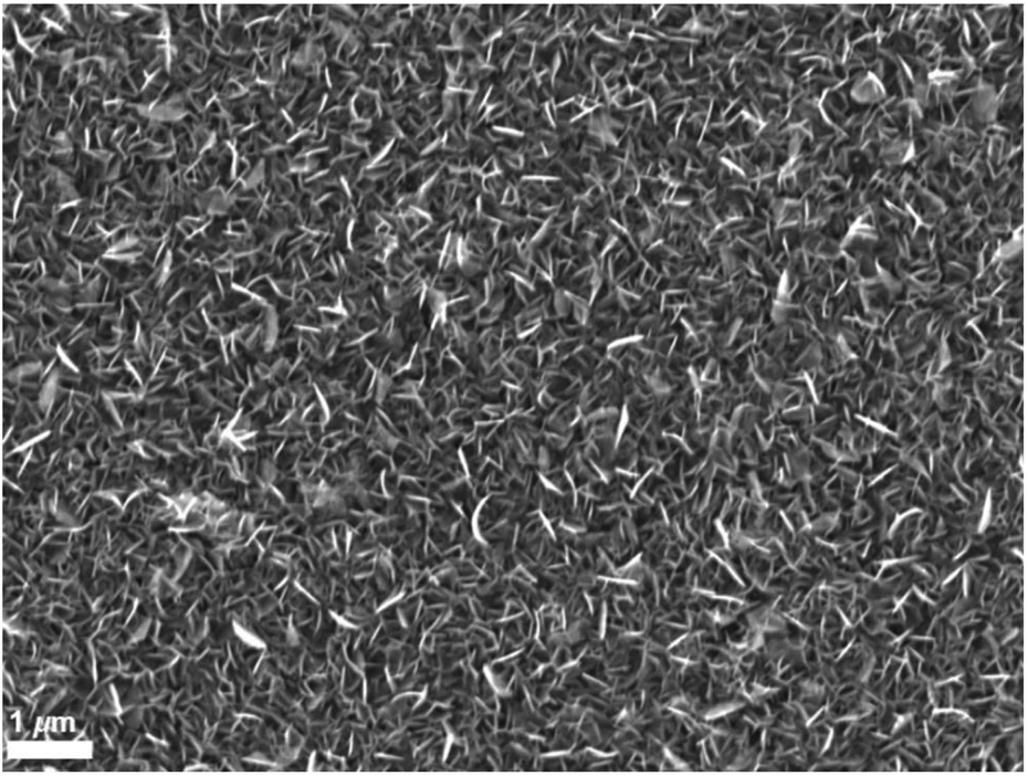
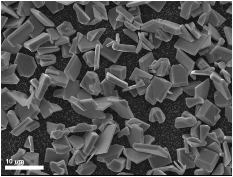
LPCVD experiments were also conducted using the tin(IV) chloride selenoether complex, [SnCl4(nBu2Se)2] (4). At 325 °C and 470 °C, a reflective silver and a black film were obtained, respectively. These were single phase SnSe2 as identified by XRD. SEM images (Fig. 7) showed regular hexagonal platelets, typical of this space group, constituting the film deposited at 325 °C. A thinner region of this film, however, showed a more disordered morphology, and it was apparent that the platelets initially lie parallel to the substrate, before more material grows upon its surface. At an elevated temperature, the crystallites appear to be a lot smaller and rougher though still ordered. EDX analysis showed a 34:66 and 35:65 Sn:Se stoichiometry for the films deposited at 325 and 470 °C respectively. There is no evidence for incorporation of Cl into the films.
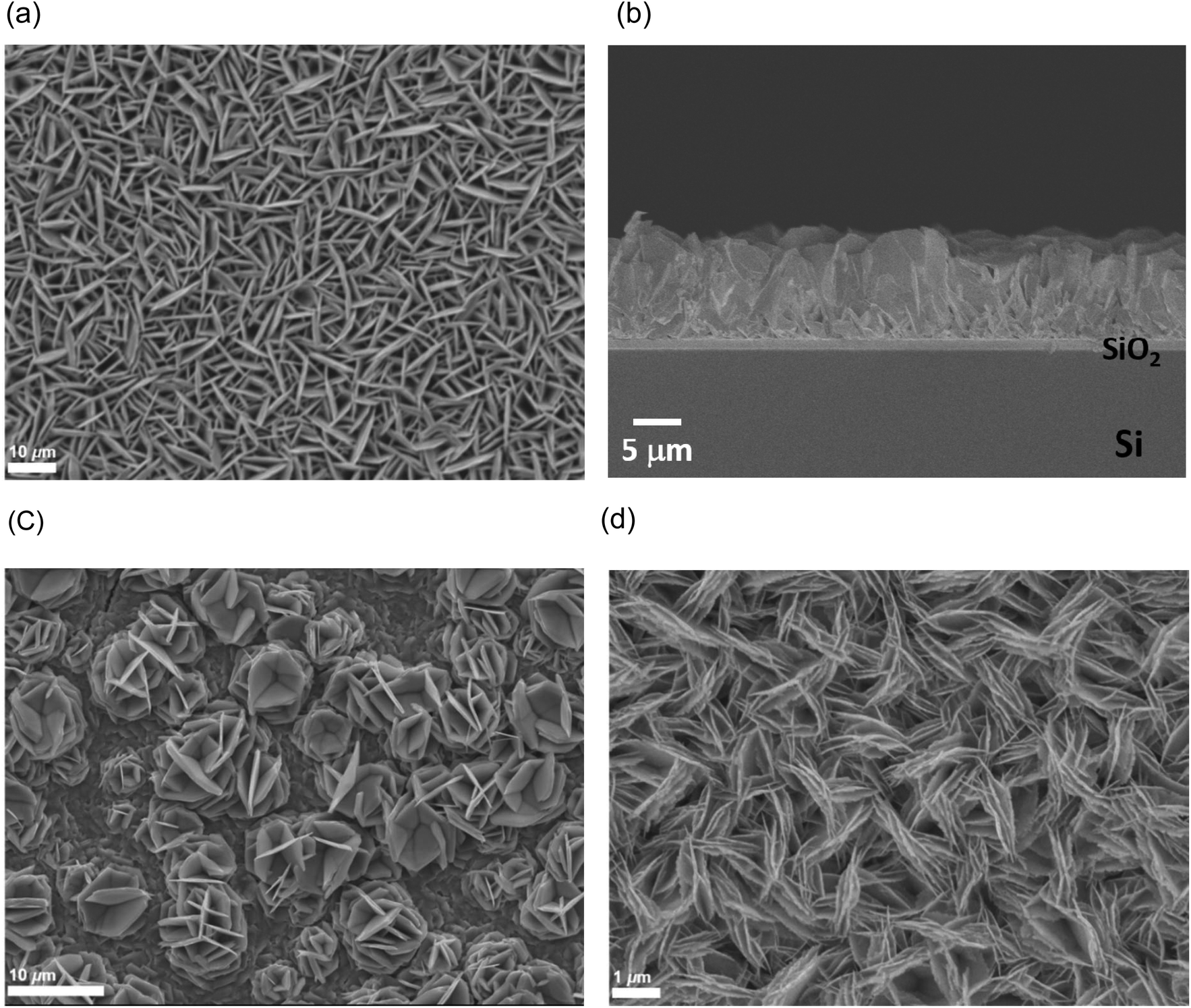 | ||
| Fig. 7 SEM images of SnSe2 deposited from [SnCl4(nBu2Se)2] at 325 °C top view (a); cross section (b); a thinner region of the film deposited at 325 °C (c); top view of a SnSe2 film deposited at 470 °C (d). | ||
XRD analysis shows that the SnSe2 crystallises in space group of Pm1 in all cases. The decrease in intensity of the 011 reflection relative to the 001 reflection (Fig. 8) suggests that the film deposited at 470 °C is thinner (and hence more strongly [001] oriented) than that deposited at 325 °C. This is borne out by cross-sectional SEM imaging and further supported by the appearance of reflections belonging to the substrate. Lattice parameters of determined for the films deposited at 325 °C and 470 °C (Table 1) are consistent with those from films deposited from our previously reported [SnCl4{nBuSe(CH2)nSenBu}] (n = 2, 3) (a = 3.81–3.83 and c = 6.14–6.16 Å).20
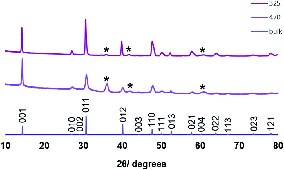 | ||
| Fig. 8 Grazing incidence XRD patterns of SnSe2 films deposited from [SnCl4(nBu2Se)2] at 325 °C (top) and 470 °C (middle), together with the stick pattern from bulk SnSe2 (bottom). The reflections marked * are from crystalline TiN underlying the top SiO2 layer on the substrate. | ||
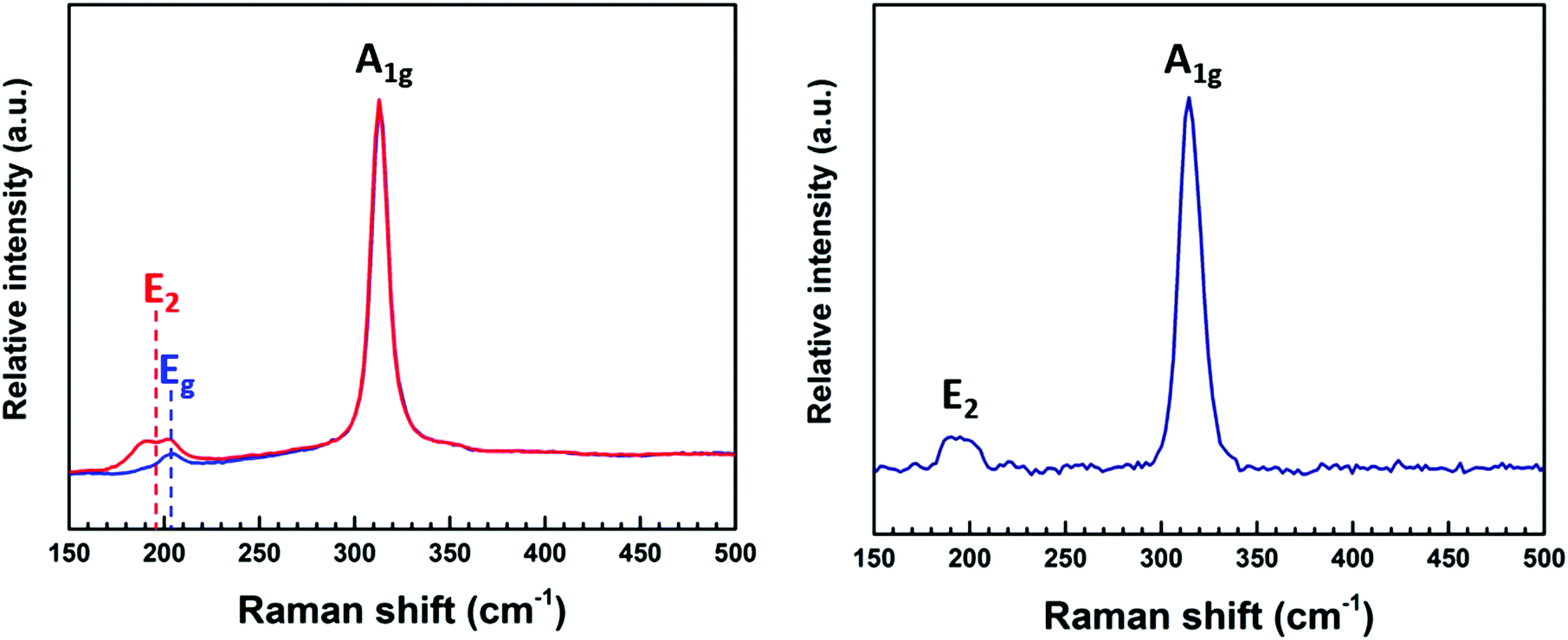
Raman spectra (Fig. 9) show an intense peak at 185 cm−1 and a weaker feature at 115 cm−1. These peaks can be assigned to the A1g and Eg modes of SnSe2, respectively.30
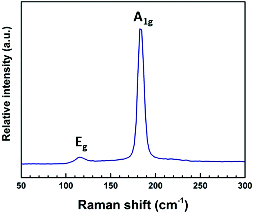 | ||
| Fig. 9 Raman spectrum of SnSe2 film deposited from (4) at 325 °C. | ||
A resistivity of 4.4(3) mΩ cm was obtained from this SnSe2 film. The value is lower than for the SnSe2 films deposited via spin-coating and annealing (∼30 mΩ cm),9 molecular beam epitaxy (22 mΩ cm)8 and CVD 210 mΩ cm.20 We also undertook further LPCVD studies to investigate film growth at higher temperatures using precursor (1), containing the bidentate diselenoether ligand.20 Similarly to the high temperature depositions using (2) described above, these showed that increasing the furnace temperature still resulted in significant SnSe2 film growth at the edge of the hot zone as before. However, where the precursor travelled further into the hotter region of the furnace, crystalline SnSe was observed. In contrast, we found no evidence for SnSe deposition using precursor (4).
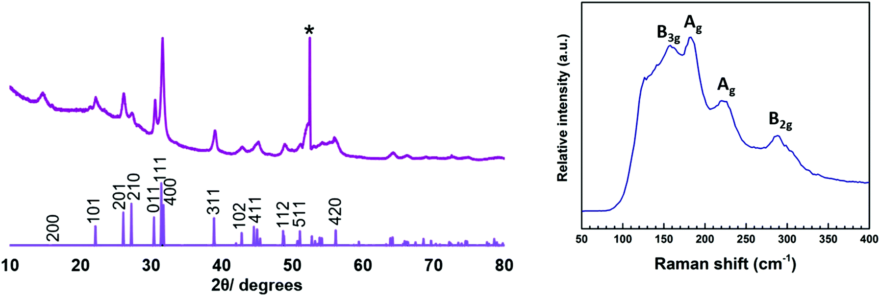
The SEM images (Fig. 10) of the SnSe deposited reveal a non-continuous, orthorhombic structure. EDX analysis of the film showed a 53:47 Sn:Se (with no Cl evident). XRD patterns (Fig. 11a) show the material to be orthorhombic SnSe. The refined lattice parameters (Table 1) match well with the literature values (a = 11.48–11.53, b = 4.06–4.09, c = 4.25–4.28).13 The Raman spectrum (Fig. 11b) shows peaks at 150, 135 and 115 cm−1, consistent with SnSe. The weak band at 185 cm−1 suggests a small SnSe2 component is present, although this is not evident in the XRD data. The peak at 115 cm−1 can be assigned to the B3g mode, 135 cm−1 the A2g mode and 150 cm−1 the A3g mode.37 The discontinuous SnSe film coverage precluded electrical measurements.
 | ||
| Fig. 10 SEM image of the polycrystalline SnSe deposited further into the hot zone of the furnace (at 588 °C) using precursor (1). | ||
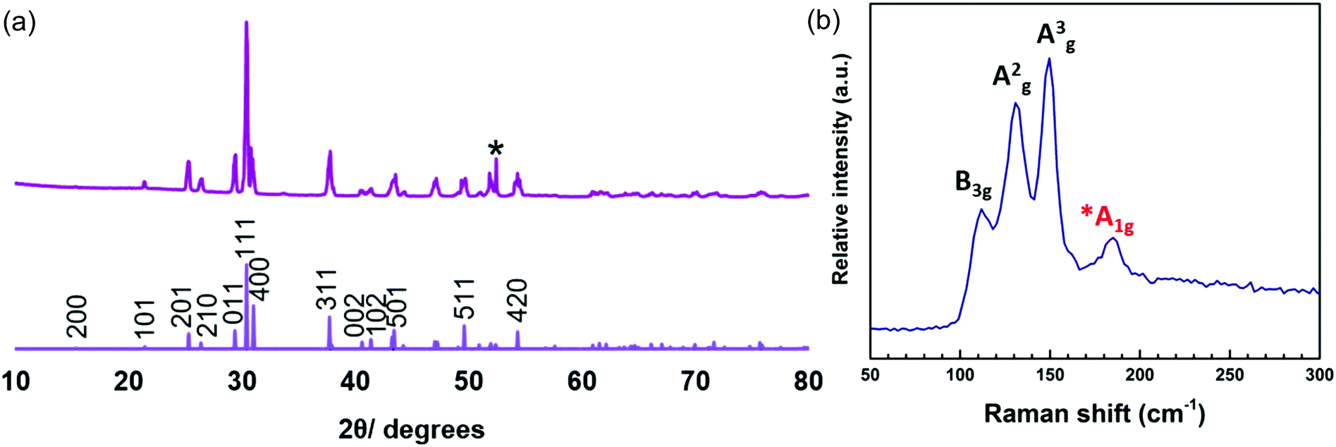 | ||
| Fig. 11 XRD pattern (a) and Raman spectrum (b) of SnSe deposited from (1). The sharp reflection marked * is from the Si underlying the SiO2 on the substrate. | ||
Conclusions
Several new molecular tin(IV) chloride complexes with monodentate and bidentate thio- and selenoether ligands bearing n-butyl terminal substituents have been prepared and evaluated as single source precursors for the LPCVD of both tin dichalcogenide (Sn(IV)) and tin monochalcogenide (Sn(II)) thin films. All four complexes have been shown to be suitable as precursors for the deposition of crystalline SnE2 thin films, the identities of which were established by grazing incidence XRD, SEM, EDX, Raman spectroscopy, and, where a single phase was obtained, van der Pauw resisitivity measurements. Using higher deposition temperatures, precursors (1) and (2) have also been shown to form tin monochalcogenide thin films, which were characterised similarly. In contrast, higher temperature LPCVD experiments using the thioether complex, (3), produces multiple phases (SnS2, Sn2S3, SnS).The resistivities measured for the SnS2 and SnS films are comparable to those reported for similar films produced from other deposition processes, whilst that for SnSe2 is at the lower end of the values reported.
Conflicts of interest
There are no conflicts to declare.Acknowledgements
We thank STFC for funding via ST/P00007X/1, STFC and EPSRC for a CASE studentship to S. L. H. (EP/M50662X/1) and EPSRC for equipment funding (EP/K009877/1). C. G. also thanks the Royal Society for Newton Alumnus Funding.References
- Y. Fu, G. Gou, X. Wang, Y. Chen, Q. Wan, J. Sun, S. Xiao, H. Huang, J. Yang and G. Dai, Appl. Phys. A, 2017, 123, 299 CrossRef.
- Y. Huang, H.-X. Deng, K. Xu, Z.-X. Wang, Q.-S. Wang, F.-M. Wang, F. Wang, X.-Y. Zhan, S.-S. Li, J.-W. Luo and J. He, Nanoscale, 2015, 7, 14093 RSC.
- I. Y. Ahmet, M. S. Hill, A. L. Johnson and L. M. Peter, Chem. Mater., 2015, 27, 7680 CrossRef CAS.
- F. K. Butt, M. Mirza, C. Cao, F. Idrees, M. Tahir, M. Safdar, Z. Ali, M. Tanveer and I. Aslam, CrystEngComm, 2014, 16, 3470 RSC.
- M. S. Mahdi, K. Ibrahim, A. Hmood, N. M. Ahmed, F. I. Mustafa and S. A. Azzez, Mater. Lett., 2017, 200, 10 CrossRef CAS.
- L.-D. Zhao, S.-H. Lo, Y. Zhang, H. Sun, G. Tan, C. Uher, C. Wolverton, V. P. Dravid and M. G. Kanatzidis, Nature, 2014, 508, 373 CrossRef CAS PubMed.
- C. Wang, Y. Chen, J. Jiang, R. Zhang, Y. Niu, T. Zhou, J. Xia, H. Tian, J. Hu and P. Yang, RSC Adv., 2017, 7, 16795 RSC.
- K.-M. Chung, D. Wamwangi, M. Woda, M. Wuttig and W. Bensch, J. Appl. Phys., 2008, 103, 83523 CrossRef.
- R. Y. Wang, M. A. Caldwell, R. G. D. Jeyasingh, S. Aloni, R. M. Shelby, H. S. P. Wong and D. J. Milliron, J. Appl. Phys., 2011, 109, 113506 CrossRef.
- P. Zhou, X. Wang, W. Guan, D. Zhang, L. Fang and Y. Jiang, ACS Appl. Mater. Interfaces, 2017, 9, 6979 CAS.
- L. S. Price, I. P. Parkin, T. G. Hibbert and K. C. Molloy, Chem. Vap. Deposition, 1998, 4, 222 CAS.
- L. S. Price, I. P. Parkin, A. M. E. Hardy, R. J. H. Clark, T. G. Hibbert and K. C. Molloy, Chem. Mater., 1999, 11, 1792 CrossRef CAS.
- N. D. Boscher, C. J. Carmalt, R. G. Palgrave and I. P. Parkin, Thin Solid Films, 2008, 516, 4750 CrossRef CAS.
- S. L. Benjamin, C. H. de Groot, C. Gurnani, A. L. Hector, R. Huang, E. Koukharenko, W. Levason and G. Reid, J. Mater. Chem. A, 2014, 2, 4865 CAS.
- R. Huang, S. L. Benjamin, C. Gurnani, Y. Wang, A. L. Hector, W. Levason, G. Reid and C. H. de Groot, Sci. Rep., 2016, 6, 27593 CrossRef CAS PubMed.
- I. P. Parkin, L. S. Price, T. G. Hibbert and K. C. Molloy, J. Mater. Chem., 2001, 11, 1486 RSC.
- K. Ramasamy, V. L. Kuznetsov, K. Gopal, M. A. Malik, J. Raftery, P. P. Edwards and P. O'Brien, Chem. Mater., 2013, 25, 266 CrossRef CAS.
- J. R. Brent, D. J. Lewis, T. Lorenz, E. A. Lewis, N. Savjani, S. J. Haigh, G. Seifert, B. Derby and P. O'Brien, J. Am. Chem. Soc., 2015, 137, 12689 CrossRef CAS PubMed.
- S. D. Reid, A. L. Hector, W. Levason, G. Reid, B. J. Waller and M. Webster, Dalton Trans., 2007, 4, 4769 RSC.
- C. H. de Groot, C. Gurnani, A. L. Hector, R. Huang, M. Jura, W. Levason and G. Reid, Chem. Mater., 2012, 24, 4442 CrossRef CAS.
- D. J. Gulliver, E. G. Hope, W. Levason, S. G. Murray, D. M. Potter and G. L. Marshall, J. Chem. Soc., Perkin Trans. 2, 1984, 429 RSC.
- ICSD: Inorganic Crystal Structure Database (ICSD), Fachinformationszentrum Karlsruhe (FIZ), accessed via the EPSRC funded National Chemical Database Service hosted by the Royal Society of Chemistry.
- S. Grazulis, D. Chateigner, R. T. Downs, A. F. Yokochi, M. Quiros, L. Lutterotti, E. Manakova, J. Butkus, P. Moeck and A. Le Bail, J. Appl. Crystallogr., 2009, 42, 726 CrossRef CAS PubMed.
- S. E. Dann, A. R. J. Genge, W. Levason and G. Reid, J. Chem. Soc., Dalton Trans., 1996, 4471 RSC; S. E. Dann, A. R. J. Genge, W. Levason and G. Reid, J. Chem. Soc., Dalton Trans., 1997, 2207 RSC; A. R. J. Genge, W. Levason and G. Reid, J. Chem. Soc., Dalton Trans., 1997, 4549 RSC.
- L. Batt, in The Chemistry of Organic Selenium and Tellurium compounds, ed. S. Patai and Z. Rappoport, Wiley, NY, 1986, vol. 1, ch. 4 Search PubMed.
- C. T. Knight and A. E. Merbach, Inorg. Chem., 1985, 24, 576 CrossRef CAS.
- Y. Kumagai, L. A. Burton, A. Walsh and F. Oba, Phys. Rev. Appl., 2016, 6, 1 Search PubMed.
- R. M. Hazen and L. W. Finger, Am. Mineral., 1978, 63, 289 CAS.
- J. R. Guenter and H. R. Oswald, Naturwissenschaften, 1968, 55, 177 CrossRef CAS.
- D. Walsh, S. Jandl and J. Harbec, J. Phys. C: Solid State Phys., 1980, 13, 125 CrossRef.
- A. J. Smith, P. E. Meek and W. Y. Liang, J. Phys. Chem. C, 1977, 1321, 1321 CrossRef.
- A. Voznyi, V. Kosyak, A. Opanasyuk, N. Tirkusova, L. Grase, A. Medvids and G. Mezinskis, Mater. Chem. Phys., 2016, 173, 52 CrossRef CAS.
- L. Amalraj, C. Sanjeeviraja and M. Jayachandran, J. Cryst. Growth, 2002, 234, 683 CrossRef CAS.
- K. Kourtakis, J. Di Carlo, R. Kershaw, K. Dwight and A. Wold, J. Solid State Chem., 1988, 76, 186 CrossRef CAS.
- K. T. Ramakrishna Reddy, P. Purandhara Reddy, P. K. Datta and R. W. Miles, Thin Solid Films, 2002, 403–404, 116 CrossRef CAS.
- T. Gotoh, Phys. Status. Solidi A, 2016, 213, 1869 CrossRef CAS.
- S. Luo, X. Qi, H. Yao, X. Ren, Q. Chen and J. Zhong, J. Phys. Chem. C, 2017, 121, 4674 CAS.
Footnote |
| † Electronic supplementary information (ESI) available: 1H, 13C{1H}, 77Se{1H} and 119Sn NMR and IR spectroscopic data for each of the new complexes, together with their TGA profiles, EDX analyses for the SnE2 and SnE films and SEM, XRD and Raman spectra for the films obtained by LP CVD using (3) at elevated temperature. See DOI: 10.1039/c7dt03848h |
| This journal is © The Royal Society of Chemistry 2018 |