Tellurene: its physical properties, scalable nanomanufacturing, and device applications
Abstract
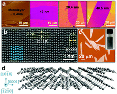
Tellurium (Te) has a trigonal crystal lattice with inherent structural anisotropy. Te is multifunctional, e.g., semiconducting, photoconductive, thermoelectric, piezoelectric, etc., for applications in electronics, sensors, optoelectronics, and energy devices. Due to the inherent structural anisotropy, previously reported synthetic methods predominantly yield one-dimensional (1D) Te nanostructures. Much less is known about 2D Te nanostructures, their processing schemes, and their material properties. This review focuses on the synthesis and morphology control of emerging 2D tellurene and summarizes the latest developments in understanding the fundamental properties of monolayer and few-layer tellurene, as well as the recent advances in demonstrating prototypical tellurene devices. Finally, the prospects for future research and application opportunities as well as the accompanying challenges of 2D tellurene are summarized and highlighted.

- This article is part of the themed collection: 2D nanomaterials: beyond graphene and transition metal dichalcogenides


 Please wait while we load your content...