
Chemical sensing with 2D materials
Cosimo
Anichini†
a,
Włodzimierz
Czepa†
bc,
Dawid
Pakulski†
abc,
Alessandro
Aliprandi
a,
Artur
Ciesielski
 *a and
Paolo
Samorì
*a
*a and
Paolo
Samorì
*a
aUniversité de Strasbourg, CNRS, ISIS, 8 alleé Gaspard Monge, 67000 Strasbourg, France. E-mail: samori@unistra.fr; ciesielski@unistra.fr
bFaculty of Chemistry, Adam Mickiewicz University, Umultowska 89b, 61614 Poznań, Poland
cCentre for Advanced Technologies, Adam Mickiewicz University, Umultowska 89c, 61614 Poznań, Poland
First published on 25th June 2018
Abstract
During the last decade, two-dimensional materials (2DMs) have attracted great attention due to their unique chemical and physical properties, which make them appealing platforms for diverse applications in opto-electronic devices, energy generation and storage, and sensing. Among their various extraordinary properties, 2DMs possess high surface area-to-volume ratios and ultra-high surface sensitivity to the environment, which are key characteristics for applications in chemical sensing. Furthermore, 2DMs’ superior electrical and optical properties, combined with their excellent mechanical characteristics such as robustness and flexibility, make these materials ideal components for the fabrication of a new generation of high-performance chemical sensors. Depending on the specific device, 2DMs can be tailored to interact with various chemical species at the non-covalent level, making them powerful platforms for fabricating devices exhibiting a high sensitivity towards detection of various analytes including gases, ions and small biomolecules. Here, we will review the most enlightening recent advances in the field of chemical sensors based on atomically-thin 2DMs and we will discuss the opportunities and the challenges towards the realization of novel hybrid materials and sensing devices.
 Cosimo Anichini | Cosimo Anichini obtained his MSc degree from the University of Bologna in 2016 under the supervision of Prof. Alberto Credi. After a research internship in the group of Prof. Paolo Samorì when he worked on the development of transparent and flexible electrodes for (opto)electronic devices, he joined the group as a PhD candidate in 2017. His current research interest is focused on the development of novel devices for sensing and (opto)electronics based on the hybrid assembly of 2D and organic/inorganic materials. |
 Włodzimierz Czepa | Włodzimierz Czepa received his MSc degree in Chemistry from Adam Mickiewicz University (AMU) in Poznań, Poland (2017), under the supervision of Prof. Violetta Patroniak. He is currently a PhD student at the Centre for Advanced Technologies of AMU, working on the chemical modification of two-dimensional layered materials and their applications in adsorption systems and sensing devices under the supervision of Dr Artur Ciesielski. |
 Dawid Pakulski | Dawid Pakulski received his MSc degree from Adam Mickiewicz University in Poznań, Poland (2015). He is currently a PhD student in the frame of the “cotutelle” program at Adam Mickiewicz University in Poznań (Poland) and the University of Strasbourg (France). His current research focuses on the design and synthesis of graphene-based materials, with particular emphasis on membranes and foams for water purification and detection of heavy metal ions. |
 Alessandro Aliprandi | Dr Alessandro Aliprandi received his master's degree from the University of Ferrara. After a short stay at the University of Münster, he received his PhD degree in Chemistry from the University of Strasbourg at the Institut de Science et d’Ingénierie Supramoléculaires (I.S.I.S.), under the supervision of Prof. Luisa De Cola. His thesis was awarded with the “Prix de these de la Fondation Université de Strasbourg” in 2016. Then he carried out postdoctoral research in the group of Prof. Paolo Samorì in the same institute. In 2018 he became a CNRS research associate (IR) in the group of Prof. Luisa De Cola. His research focuses on self-assembling (electro)-luminescent transition-metal complexes as well as 2D materials for electronic applications. |
 Artur Ciesielski | Artur Ciesielski got his master's degree from Adam Mickiewicz University (Poland), followed by his PhD degree from the University of Strasbourg (France). In 2016 he became a research associate (IR) working at the Institut de Science et d’Ingénierie Supramoléculaires and Centre National de la Recherche Scientifique. More recently, he has been appointed as visiting professor at the Centre for Advanced Technologies of Adam Mickiewicz University (Poland). His current research interests include the design of supramolecular systems, the self-assembly of nanopatterns and the production and chemical modification of 2D materials by exploiting supramolecular approaches. |
 Paolo Samorì | Paolo Samorì obtained a Laurea degree in Industrial Chemistry from the University of Bologna in 1995 and a PhD in Chemistry from the Humboldt University of Berlin in 2000. After being a research scientist at the National Research Council of Bologna, he was appointed Professor of Physical Chemistry at the Université de Strasbourg. He is now Distinguished Professor and Director of the Institut de Science et d'Ingénierie Supramoléculaires (ISIS) of the Université de Strasbourg. He is a Fellow of the Royal Society of Chemistry (FRSC), a Fellow of the European Academy of Sciences (EURASC), a Member of the Academia Europaea and a Junior Member of the Institut Universitaire de France (IUF). His research interests encompass supramolecular sciences, nanochemistry and materials chemistry, with a specific focus on graphene and other 2D materials as well as functional organic/polymeric and hybrid nanomaterials for applications in opto-electronics, energy and sensing. His work has been awarded various prestigious prizes and honorary professorships. |
1 Introduction
Since the ground-breaking experiments by Geim and Novoselov on the isolation and study of the outstanding physical properties of graphene in 2004,1 the research endeavour on two-dimensional materials (2DMs) has grown exponentially, becoming a flagship in many classical fields of research such as chemistry and condensed matter physics, and it is particularly blooming in the interdisciplinary realms of nanoscience and materials science. One-atom thick graphene is arguably the most glorified material of the last decade; its fascinating physico-chemical properties have spread beyond the academic community and drawn the attention of world-leading chemical and materials oriented companies as well as public institutions, especially since graphene-based products are going on sale.2 This so-called ‘graphene rush’ has triggered the pursuit of atomically thin sheets of other layered materials, such as semiconducting transition metal dichalcogenides (TMDs),3 boron nitride and, more recently, MXenes, which include transition metal carbides, nitrides and carbonitrides,4 and phosphorene.5–7 The chemical and structural diversities of these 2DMs, whose properties are indeed dictated by their dimensionality,8 offer immense opportunities for fundamental and applied research. Different optical and electronic properties may be achieved ranging from the exceptional semi-metallic conductivity of graphene9,10 to the semiconducting characteristics of some TMDs that possess sizeable and tuneable bandgaps, which change from indirect (bulk material) to direct (single layer form).11 This also results in unique photoluminescence properties,12 thus making such materials suitable for diverse applications such as transistors, photodetectors, electroluminescent devices and luminescent probes. The richness of their electronic and optical properties, which can also be engineered by chemical functionalization, combined with their 2D nature, i.e. their extremely high surface area-to-volume ratios, makes such materials extremely appealing in the field of sensing, ranging from the quantitative detection of gases and metals (alkali and heavy metals) to biologically relevant molecules (e.g. glucose and DNA). Noteworthily, unlike classical digital sensors, 2DM-based sensors do not possess physical gates for selectively reacting with the targeted species (gas molecules,13,14 metal ions or biomolecules15,16).The interaction between 2DMs’ sheets and molecules/ions is accompanied by the adjustment of the properties of both the initial components. Such interaction can occur via the physical adsorption, i.e. physisorption, of molecular units onto the basal planes of 2DMs’ sheets through non-covalent interactions, or through the chemical adsorption, i.e. chemisorption, of reactive species undergoing chemical reactions with 2DMs to form covalent bonds onto their basal planes. In the field of sensing, non-covalent interactions may be preferred when a quick response and a fast recovery rate are required (i.e. real-time monitoring), yet the weakness of the supramolecular forces can be disadvantageous when biomolecules (i.e. enzymes) need to be immobilized on the surface and to be stable during the assay (i.e. in buffered saline solution), thus making covalent linkages more suitable.
The physisorption of molecules onto a surface depends on the nature of both the analyte and surface; for example, graphene is an extended honeycomb network of sp2 hybridized carbon atoms characterized by a long-range π-conjugation. Consequently, non-covalent intermolecular interactions involving π-systems are pivotal in the recognition events since subtle changes in the electronic characteristics of the π systems can lead to modifications of the structure and properties,17,18 as well as they may enhance the stability of the physisorbed compounds as observed for proteins, and enzyme–drug and DNA–protein complexes.19,20 The understanding of the nature of π-complexes has indeed high importance for graphene based sensors since the gas–π interaction,21 H–π interaction,22–25 π–π interaction,26–31 cation–π interaction,32–39 and anion–π interaction26,40–50 possess different strengths, which are determined by a combination of attractive and repulsive forces. Compared to graphene, the family of TMDs, which includes molybdenum disulfide (MoS2), tungsten disulfide (WS2), molybdenum diselenide (MoSe2) and tungsten diselenide (WSe2) as the most studied, has not been investigated extensively from this point of view. However, in the case of MoS2 it has been demonstrated that the physisorption onto its basal plane is mainly driven by electromagnetic interactions (e.g. electrostatic and van der Waals).51,52 More generally, 2DMs produced by means of different methods can be very different due to the presence of structural defects, which leads to different behaviours, and consequently different performances in the final sensing device. In the past years the term “defects”53–57 has become a keyword in the field of 2DMs since the presence of defects plays a major role in modifying the properties of 2DMs. Although defects might have a negative implication when one targets applications in fast opto-electronics, well-designed defects might lead to new and tuneable properties, opening a wide range of interesting applications that pristine materials cannot afford such as enhanced electron transfer rates and electrochemical activity as observed for graphene based electrochemical sensors.58 Lattice vacancies affect the electronic properties of the TMD sheets, by lowering their charge carrier mobility and density59,60 as well as triggering photoluminescence61,62 and modifying chemical reactivity.63 In graphene the defects within the honeycomb network of C![[double bond, length as m-dash]](https://www.rsc.org/images/entities/char_e001.gif) C, whose number depends mainly on the protocol employed for its fabrication, typically consists of point defects, i.e. the absence of some sp2 carbon atoms, and/or the presence of carbon atoms with sp3 hybridization. The carbon atoms surrounding these defects are electronically perturbed; thus they exhibit different electronic structures; therefore, they are chemically activated for further chemical reactions. In other words, the presence of point defects enhances the chemical reactivity of graphene.64 The sp2 carbon atoms of graphene can react with highly reactive free radicals, such as those produced by diazonium salts65–67 or benzoyl peroxide;68 as well as dienophiles which react with the CC of graphene through a 1,3-dipolar cycloaddition.69 However, a massive introduction of defects can be achieved by exposing graphite to strong oxidizing agents,70 resulting in the formation of graphite oxide (GO). The latter when immersed in water tends to spontaneously exfoliate into single layers of graphene oxide due to the negative charged oxygen functionalities decorating both the basal plane and edges.71 Such material is probably the most investigated 2DM in the field of sensing72–76 because of its ease of functionalization. The negative charges on its surface can interact non-covalently with a wide range of positively charged molecules; for example, outstanding sorption properties for heavy metal cations have been reported.77,78 Moreover, the oxygen functionalities, which consist mostly of hydroxyl and epoxy groups exposed on the basal plane and carboxy and carbonyl functionalities located at the sheet edges,79,80 are extremely reactive, thus allowing further modification of GO.81,82 Importantly, the electrical conductivity can be to a great extent restored and tuned during the reduction step of the functionalized graphene oxide (fGO),83 making it an extremely versatile material for sensing with electrical readouts. The use of defects to introduce functionalities has also been successfully extended to the family of TMDs, where the presence of chalcogen deficiency can be used to decorate the surface of the 2DM with different functionalities. For example, reactive sulphur vacancies in MoS2 may simply arise during the exfoliation process59,84 or be introduced on purpose electrochemically85 or by ion-beam irradiation.86 These reactive sites can readily react with sulphur-containing moieties such as alkanethiol molecules, resulting in the formation of covalent bonds.86–88 Alternatively, defects can be further expanded into (sub)-nanometre sized pores, transforming the 2DMs into permselective membranes89 or ultrasensitive sensors even able to sequence DNA.90,91 Such a property can be further tuned and harnessed to achieve enhanced permselectivity by controlled chemical functionalization of both pore edges and the surface in a post-process chemical treatment.89 As already anticipated, the 2D nature of such materials offers several advantages in the field of sensing since the atomic thickness provides a direct interaction of all the atoms with the analyte, while the large lateral size not only guarantees a large active surface for the sensing event, but also facilitates the assembly of the device, as demonstrated for field-effect transistors (FETs), i.e. by enabling better contact with metal electrodes and better control over the channel structures.92 Obviously, the architecture of the sensing device depends on which properties of the 2DMs the analytes affect mostly as well as on the nature of both the 2DM and the analyte. Electrochemical sensors based on graphene have been probably the most investigated so far since they provide a direct electrical response. Graphene93 offers indeed a large electrochemical window (up to 2.5 V),72 thus enabling the detection of molecules with high reduction or oxidation potentials (e.g. nucleic acids), and good electrocatalytic activities for many redox reactions.94 Furthermore, due to its ambipolar character, the functionalization with both electron withdrawing and donating groups can lead to chemical gating, resulting in a change in the conductivity of the material.95 The combination of the atomic thickness of the 2DMs with the chemical gating that results when the surface potential is changed due to the binding of molecules has led to the generation of new FET sensors based on 2DMs, as recently reviewed by Mao et al.92 Interestingly, in such kinds of sensors, 2D semiconducting materials outperform their conducting counterparts since the presence of a finite band gap decreases the initial conductance inside the channel, thus improving the signal-to-noise ratio. Consequently, the performance of the device is mainly dictated by the band gap, which can be tuned by defect engineering and doping, as well as by playing with the thickness of the material, opening a wide range of opportunities, as recently demonstrated by Cui et al.96 in a phosphorene-based FET gas sensor.
C, whose number depends mainly on the protocol employed for its fabrication, typically consists of point defects, i.e. the absence of some sp2 carbon atoms, and/or the presence of carbon atoms with sp3 hybridization. The carbon atoms surrounding these defects are electronically perturbed; thus they exhibit different electronic structures; therefore, they are chemically activated for further chemical reactions. In other words, the presence of point defects enhances the chemical reactivity of graphene.64 The sp2 carbon atoms of graphene can react with highly reactive free radicals, such as those produced by diazonium salts65–67 or benzoyl peroxide;68 as well as dienophiles which react with the CC of graphene through a 1,3-dipolar cycloaddition.69 However, a massive introduction of defects can be achieved by exposing graphite to strong oxidizing agents,70 resulting in the formation of graphite oxide (GO). The latter when immersed in water tends to spontaneously exfoliate into single layers of graphene oxide due to the negative charged oxygen functionalities decorating both the basal plane and edges.71 Such material is probably the most investigated 2DM in the field of sensing72–76 because of its ease of functionalization. The negative charges on its surface can interact non-covalently with a wide range of positively charged molecules; for example, outstanding sorption properties for heavy metal cations have been reported.77,78 Moreover, the oxygen functionalities, which consist mostly of hydroxyl and epoxy groups exposed on the basal plane and carboxy and carbonyl functionalities located at the sheet edges,79,80 are extremely reactive, thus allowing further modification of GO.81,82 Importantly, the electrical conductivity can be to a great extent restored and tuned during the reduction step of the functionalized graphene oxide (fGO),83 making it an extremely versatile material for sensing with electrical readouts. The use of defects to introduce functionalities has also been successfully extended to the family of TMDs, where the presence of chalcogen deficiency can be used to decorate the surface of the 2DM with different functionalities. For example, reactive sulphur vacancies in MoS2 may simply arise during the exfoliation process59,84 or be introduced on purpose electrochemically85 or by ion-beam irradiation.86 These reactive sites can readily react with sulphur-containing moieties such as alkanethiol molecules, resulting in the formation of covalent bonds.86–88 Alternatively, defects can be further expanded into (sub)-nanometre sized pores, transforming the 2DMs into permselective membranes89 or ultrasensitive sensors even able to sequence DNA.90,91 Such a property can be further tuned and harnessed to achieve enhanced permselectivity by controlled chemical functionalization of both pore edges and the surface in a post-process chemical treatment.89 As already anticipated, the 2D nature of such materials offers several advantages in the field of sensing since the atomic thickness provides a direct interaction of all the atoms with the analyte, while the large lateral size not only guarantees a large active surface for the sensing event, but also facilitates the assembly of the device, as demonstrated for field-effect transistors (FETs), i.e. by enabling better contact with metal electrodes and better control over the channel structures.92 Obviously, the architecture of the sensing device depends on which properties of the 2DMs the analytes affect mostly as well as on the nature of both the 2DM and the analyte. Electrochemical sensors based on graphene have been probably the most investigated so far since they provide a direct electrical response. Graphene93 offers indeed a large electrochemical window (up to 2.5 V),72 thus enabling the detection of molecules with high reduction or oxidation potentials (e.g. nucleic acids), and good electrocatalytic activities for many redox reactions.94 Furthermore, due to its ambipolar character, the functionalization with both electron withdrawing and donating groups can lead to chemical gating, resulting in a change in the conductivity of the material.95 The combination of the atomic thickness of the 2DMs with the chemical gating that results when the surface potential is changed due to the binding of molecules has led to the generation of new FET sensors based on 2DMs, as recently reviewed by Mao et al.92 Interestingly, in such kinds of sensors, 2D semiconducting materials outperform their conducting counterparts since the presence of a finite band gap decreases the initial conductance inside the channel, thus improving the signal-to-noise ratio. Consequently, the performance of the device is mainly dictated by the band gap, which can be tuned by defect engineering and doping, as well as by playing with the thickness of the material, opening a wide range of opportunities, as recently demonstrated by Cui et al.96 in a phosphorene-based FET gas sensor.
While a direct electrical response is generally preferred for practical applications, the interactions of 2DMs with analytes give rise to interesting optical phenomena such as the modulation of their photoluminescence properties, opening up a wide range of opportunities. Graphene and GO are known to be highly efficient fluorescence quenchers compared to organic compounds; thus Förster resonance energy transfer (FRET) sensors have attracted increasing interest in the past few years especially for biomedical applications since they can be used to measure precisely nanometre-scale distance and changes both in vivo and in vitro,97 resulting in nanobiosensors with excellent sensitivity, selectivity, and biostability.98 Even a single-layer MoS2 nanosheet possesses high fluorescence quenching efficiency, and by taking advantage of such a characteristic, it has been exploited as a sensing platform for the detection of DNA and small molecules.99 However, the use of 2DMs in FRET is not limited to energy acceptors since an appropriate functionalization may result in photoluminescent flakes, which can act as energy donors and be quenched by more electron deficient molecules such as nitro compounds, which are common constituents to prepare powerful explosives.100
The use of 2DMs as substrates for enhancing the Raman signals of adsorbed molecules represented a major breakthrough in the field of sensing.101,102 Different Raman vibrational modes can be enhanced depending on which layered material the molecule is adsorbed onto. Surface enhanced Raman spectroscopy (SERS) is mainly employed to explore the detection of chemical and biological species103–106 due its high sensitivity (even down to single molecules)107,108 and the bar-code like reading that comes from the narrow vibrational bands in the Raman spectrum. Different Raman enhancement mechanisms have been proposed for different 2DMs; however, like in the previous examples, surface modification109 and the thickness110 play fundamental roles in terms of selectivity and Raman signal enhancement.
The intensive research on 2DMs for sensing application has been further motivated by their intrinsic mechanical properties such as robustness, flexibility, and lightweight, which make the realization of portable and wearable sensors with tremendous impact on our society possible, enabling the monitoring of wearers’ health, fitness, and their surroundings.111 The development of wearable chemical sensors faces multiple challenges on various fronts such as power, analytical procedures, communication, data acquisition, processing and security. Nevertheless, several examples of flexible graphene-based wearable gas and chemical sensors have been recently reviewed,112 and a wearable patch for sweat-based diabetes monitoring and feedback therapy has also been reported,113 which combines a heater and temperature, humidity, glucose and pH sensors.
Looking forward to the emergence of portable and ultrasensitive sensors based on 2DMs, in this Review article we discuss the recent advances in gas, alkali and heavy metal sensing as well as relevant chemical entities, emphasizing the performances of the different sensor devices based on 2DMs in terms of sensitivity, selectivity, robustness and response times, by focusing on the device preparation and their suitability as wearable sensors. Each section will start with a general introduction to the sensing towards a specific analyte (gases, metals or chemically relevant molecules), and will be followed by a detailed discussion on the smartest approached strategies and the best recent achievements obtained for various 2DMs ranging from graphene to MXenes. For each 2DM we classify the sensors on the basis of the type of signal transduction; in particular, we focus on electrochemical, FET, fluorescent and SERS sensors. While presenting remarkable examples of chemical sensors, we will pay specific attention to the most important figures of merit such as their sensitivity, selectivity, robustness, and response time, and to the use of strategies to minimize and ideally exclude the effects of interfering analytes, with the final aim of developing flexible sensors for wearable technology (Fig. 1).
 | ||
| Fig. 1 Schematic representation of the different molecular chemical sensors based on 2DM approaches that have been explored over the past few years. | ||
1.1 Overview on the properties of 2DMs
Graphene is an atomically thin, planar membrane of carbon atoms arranged in a honeycomb lattice whose unique properties were first investigated by Geim and Novoselov in 2004.1 Graphene can be seen as a single layer of graphite, and while the latter behaves metallically, graphene is a semi-metal featuring a unique zero band gap.114 In addition, graphene exhibits remarkable thermal and electrical conductivity and an impressive mechanical strength superior to steel.2 Graphene is particularly promising for sensing by virtue of its extremely high conductivity, and its large surface area. Despite being only one atom thick, graphene is impermeable in its pristine form, effectively blocking the passage of even the smallest molecules.115 The impermeable nature of graphene has triggered extensive studies on its application as a barrier for liquid and gas permeation,116,117 as well as on its use as a shielding material protecting metallic surfaces against corrosion.118 Such a unique property of graphene has triggered extensive efforts towards the use of graphene and other 2DMs for the design of ultrathin water-separation membranes and as platforms to absorb (heavy) metal ions. Hitherto the highest quality graphene flakes have been obtained using a top-down approach relying on mechanical exfoliation. The graphene layers are most commonly exfoliated from the bulk graphite via the “Scotch tape” method.119 Unfortunately, the flakes produced with such a method have high quality, yet very limited lateral size. Large area and high-quality mono- and few-layer thick graphene sheets can be obtained by two bottom-up approaches: chemical vapour deposition (CVD) and epitaxial growth. CVD graphene is usually obtained through a catalytic decomposition of hydrocarbons (usually methane) on a hot (∼1000 °C) metal surface (Cu, Ni and Co) under vacuum.120 Since the graphene grows directly onto the metal surface, different techniques have been developed to transfer it onto dielectric substrates.121 Epitaxial growth is another method to obtain large and uniform high-quality graphene films.122 Typically, SiC is heated under high vacuum at high temperature (>1200 °C); this allows the surface silicon atoms to evaporate, yielding the rearrangement of the carbon atoms to form a graphene layer. Mechanical exfoliation makes it possible to obtain high quality graphene monolayers, but the very low throughput and yield of the so-obtained graphene flakes hinder any industrial application, while CVD and epitaxial growth allow obtaining large-area graphene monolayers, although the production costs remain high. The production of GO followed by its reduction is a high throughput, easily scalable and cheap method to obtain a large amount of graphene.123 It is, however, fair to note that reduced graphene oxide (rGO) is less conductive and has numerous structural defects and residual functional groups compared to pristine graphene, yet its presence could offer a clear route for improvement of the sensing capabilities as already discussed.124 Similarly, GO has a higher number of oxygen functional groups, but it is an electrical insulator.123 A compromise in terms of the quality of the flakes and yield is offered by the liquid-phase exfoliation (LPE) of graphite: graphene flakes dispersed in water/surfactants or organic solvents can be obtained with the aid of ultrasonication,125,126 shear mixing127 or an electrochemical approach.128Alongside graphene, transition metal dichalcogenides are the most studied 2DMs. TMDs are semiconductors of the type MX2, where M is a transition metal atom (such as Mo, W, Re and others belonging to groups 4, 5 and 10) and X is a chalcogen atom (such as S, Se or Te); these materials that exist in the bulk form can be exfoliated, yielding 2D monolayers in which one atomic layer of the metal is sandwiched between two layers of X atoms. TMDs are promising materials for use in electronic devices,129,130 energy storage131 and sensors132–134 due to their unique chemical and physical properties, including semiconducting properties, high surface area-to-volume ratios and absorption coefficients, adjustable and direct band gaps and availability of reactive sites for redox reactions.135 The chemical versatility of TMDs and their reactivity together with their natural abundance result in the ever growing interest in those materials.135 Although a majority of TMDs exhibit similar structures, their opto-electronic properties are diverse. In particular, the band gaps of TMDs range from insulating HfS2 to conductive VSe2.135 Noteworthily, 2D TMDs exhibit two different crystal phases: a trigonal prismatic and an octahedral phase, usually denoted as 2H and 1T phases, respectively. In Mo- and W-based TMDs the 2H phase is thermodynamically stable and has semiconductive properties, while the 1T phase displays metallic properties. Other TMDs present a stable distorted octahedral phase, usually referred to as a 1T’ phase.136 The most investigated TMDs are MoS2, MoSe2, WS2, WSe2, ReS2 and ReSe2. Among them, MoS2 is considered as the most promising material as it exhibits various physico-chemical properties including fast electron transfer, good conductivity and a quenching ability and it is abundant in nature as molybdenite. Multiple preparation techniques have been reported to obtain nanosized MoS2 including LPE,137 chemical vapour deposition,138,139 and lithium intercalation.99,140,141 LPE makes it possible to obtain dispersions of MoS2 nanosheets and other TMDs in higher yield and low cost. However, the obtained materials are usually quite thick and feature limited lateral dimensions.142 Larger mono- and few layers thick MoS2 of good quality can be produced by CVD143 directly on various substrates, including Si/SiO2.144–147 Semiconducting MoS2 exhibits a thickness-dependent band gap, ranging from 1.3 eV for bulk MoS2 to 1.9 eV for isolated monolayers,148 good conductivity and fast electron transfer. MoS2 is currently considered as one of the most preferable materials for chemical sensing applications, predominantly due to available edges that facilitate electron transfer.3,149 Moreover, it can be easily produced on a large scale and dispersed in numerous solvents to obtain desired structures.137,150 Layered tungsten disulphide (WS2) nanosheets are one among the newly emerging TMDs, which consist of S–W–S sandwich structures. WS2 nanosheets have been the focus of intense research effort as a catalyst, a semiconducting material for field-effect transistors, an active material in lithium-ion batteries, etc. Ambipolar WSe2 has a similar trigonal lattice and a 1.6 eV band gap (in the monolayer). Finally, ReS2, ReSe2 and PtSe2 are recently explored TMDs, characterized by a highly distorted triclinic structure which endows them with extremely anisotropic optical, mechanical and electrical properties.151 Mono- and few-layer ReS2 and ReSe2 can be obtained by mechanical exfoliation and CVD.152
Similar in structure to TMDs, SnS2 is a layered material possessing a triclinic structure, which can be exfoliated into mono- and few-layers with semiconducting properties.135 Compared to TMDs, SnS2 exhibits a higher electronegativity, which can potentially enhance the absorption sites and the sensing capabilities.
Among the emerging 2DMs, black phosphorus (BP) has been recently re-discovered as a 2DM under the commonly used name of phosphorene. This material, which is, in analogy to graphene, a single honeycomb layer of the layered phosphorus allotrope can be obtained via mechanical or liquid exfoliation and presents remarkable electrical properties of a tuneable direct band gap and high mobility.153 BP exhibits a relatively low energy band gap, which depends on the number of layers and ranges from 0.3 to 1.5 eV.154,155 BP exhibits fascinating optical and electronic properties such as size dependent optical response and anisotropic electrical conductivity, which simplifies characterization and segregation methods and makes BP a promising material for various electrical applications.156,157 BP has already found several applications as FETs, photodetectors, solar cells and gas sensors.158–161 However, its application in devices is limited by the very low material's stability when exposed to air or water.162 Such a negative characteristic can become an advantage when fabricating chemical sensors.
Hexagonal boron nitride (hBN) is a synthetic polymorph of boron nitride with a layered structure analogous to graphite. Similarly to graphene, hBN WS2 exhibits a two-dimensional honeycomb-like structure with strong covalent bonds in the plane. It is characterized by a relatively high band gap ranging from 3.6 to 7.1 eV, which determines its insulating properties.163,164 This feature provides transparency in the visible and near-IR regions, extending its application potential.165 The weakly bonded layers can be exfoliated down to monolayer hBN, which has not only electrical insulating properties, but also high thermal conductivity, mechanical strength, hardness and chemical stability.166 The production method strictly determines the 2D hBN nanosheets’ crystallinity, structure and other physical and chemical properties. Multiple methods have been exploited for hBN production including mechanical exfoliation,167,168 liquid exfoliation137,169–171 and chemical vapour deposition.172–174 Features such as good thermal conductivity, low toxicity, high mechanical strength, and atomically smooth surface makes BN a good candidate for sensing applications.
The large family of 2DMs also includes early transition metal carbides/nitrides (MXenes). This novel class of 2DMs shows promising properties toward a range of applications. MXene nanosheets originate from the MAX phases which constitute a class of nitrides and carbides, in which M is an early transition metal, A is an element from group 13 or 14 of the periodic table, X is C and/or N. The MXene layers are obtained from the MAX phase by the removal of the element A, which is intercalated between MXene layers of the crystal, by treatment with HF and further sonication.175 MXenes display good electronic conductivity and a unique morphology, making them suitable for energy storage,176 electrochemical capacitors177 and chemical sensors.178,179
In the field of sensing it is generally preferred to make use of non-covalent interactions between the sorbent, i.e. the active material, and the analyte to ensure a quick response and a fast recovery rate (i.e. real-time monitoring). The use of pristine 2DM nanosheets has some drawbacks. A major limitation is their poor porosity, which limits the number of available recognition sites. In particular, 2DM nanosheets produced via LPE exhibit a strong tendency to self-aggregate and form even micron-sized stacked structures. Moreover, nanosheets produced via LPE exhibit low charge carrier as well as low field-effect mobility.
Alongside the capacity of pristine 2DMs to detect various analytes, extensive efforts have been devoted towards the development of 2DM-based sensors through the non-covalent functionalization of 2DMs with both inorganic and organic moieties which act as spacers/pillars imposing a certain distance between adjacent sheets. This results in an enhanced porosity of 2DM-based composites, which determines a greater sensitivity for the analyte of choice. Such an approach enables the tailoring of the properties of 2DM-based sensors, which could preserve many of the unique characteristics of the individual 2DM sheets and benefit from the presence of (in)organic moieties. Such moieties, besides acting as separators, can by design incorporate the receptor of the analyte of choice, endowing the highest selectivity in the recognition and sensing process. In this context, the fabrication of 2DM-based sensors through non-covalent interactions between individual 2DM sheets is extremely appealing, as it could result in structures exhibiting a remarkable enhancement of sensitivity towards specific analytes.
2 Applications in gas sensing
A gas sensor is a device that can detect the presence and quantify the concentration of a specific gas in the atmosphere such as water vapour (humidity), organic vapours and hazardous gases.180 Gas sensors have attracted strong interest and are widely employed in environmental monitoring and emission control,181 personal and military safety,182 production control in agriculture and industry and medical diagnostics.183–185 Among the variety of materials used for gas sensing devices, metal oxides have been largely considered for their high sensitivity and low cost; however, their crucial drawbacks such as high temperature operation and large energy consumption, as well as poor selectivity, have hindered their practical application.186 Therefore, many efforts have been devoted towards developing new gas sensors with high sensitivities and low operating temperatures. Numerous active materials have been considered including conducting polymers187 and carbon nanotubes (CNTs),188 which possess interestingly low operating temperatures but suffer from long response and recovery times, poor stability, degradation and difficult processing.In the past few years 2DMs have emerged as new materials for gas sensing by virtue of their unique properties, which promise to largely improve the sensitivity of the sensors. Among 2DMs, graphene is particularly appealing, because of its low resistivity and electrical noise.189 Such characteristics enable the detection of small changes in the intrinsic resistance resulting from the interaction of graphene with gaseous species. Alongside graphene, its analogues such as TMDs (MoS2,190–193 WS2,194,195 MoSe2, etc.), layered metal oxides (MoO3,196 SnO2197,198), phosphorene,158 h-BN,199etc., have also been employed for gas sensing by exploiting their thickness dependent characteristics and semiconducting properties. Indeed, the presence of a band gap that can be modulated by the interaction with gases is a tool that enables enhanced sensitivity. Furthermore, the semiconducting properties of these materials render them suitable for integration as active components in FETs, allowing realization of low power consumption and miniaturized devices.199 In these devices, the adsorption of gases on the semiconducting material determines a change in their conductivity, which can be measured as a variation in the drain current.144 Other common gas sensing devices are chemiresistors185 and chemi-capacitors,200 in which the sensing material is interposed between two electrodes, and the gas molecules adsorbed on the surface of the material induce a change in the resistance or capacitance, which can be directly quantified.
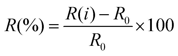
The performances of gas sensors are usually characterized by various figures of merit, with the most important being sensitivity, selectivity, stability, response and recovery times, cost, dimensions and flexibility. In this section we will define the response R(%) of a given device as the ratio between the difference in resistance (or another output) when it is operating in the presence and in the absence of the sensed gas, and the resistance in the absence of the sensed gas:
 | (1) |
2.1 Graphene-based gas sensing
The first application of graphene as a gas sensor was reported in 2007 by Novoselov et al.201 A micromechanically exfoliated graphene flake supported on a Si/SiO2 substrate was first etched in a bar shape and patterned with top gold contacts exploiting electron-beam lithography (EBL) (Fig. 2a) and later exposed to H2O, NO2, NH3 and CO gases. It was shown that the presence of gas molecules causes a doping in the graphene, changing the concentration of charge carriers. In particular, it was demonstrated that H2O and NO2 decrease the charge carrier concentration, while an increase of the carrier concentration was observed when NH3 or CO was employed (Fig. 2b). Furthermore, exploiting the Hall resistivity, changes in the number of carriers of just a single electron were investigated in the vicinity of the Dirac point. In this way, by exposing the device to very diluted NO2 gas, it was possible to sense the adsorption of a single NO2 molecule. In fact, it can be seen that the Hall resistivity varies in a step-like manner, because each NO2 molecule adsorbed/desorbed produces a variation of one electron in the number of carriers (Fig. 2c). This outstanding performance was attributed to the high carrier mobility and extremely low noise of the so patterned graphene device.
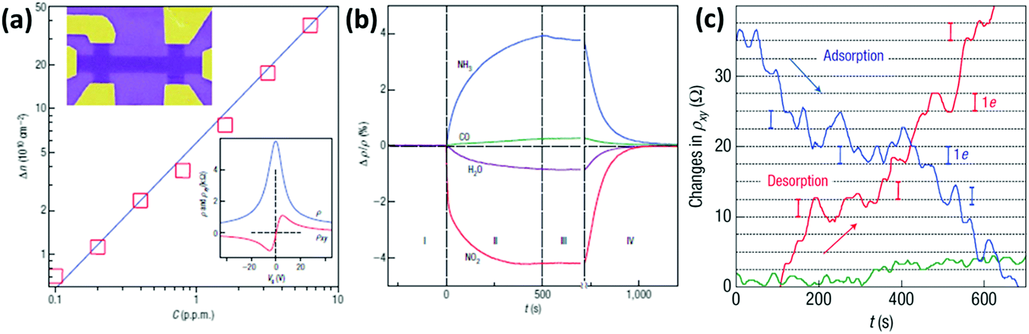 | ||
| Fig. 2 (a) Dependence of the concentration of charge carriers (Δn) in single-layer graphene when exposed to different concentrations (C) of NO2. Upper inset: Scanning electron microscopy (SEM) image in false colours of this device (the device is 1 μm wide). Lower inset: Characterization of the graphene device using the electrical field-effect. (b) Changes in resistivity caused by graphene's exposure to 1 ppm of various gases, highlighting the positive or negative doping effects. (c) Changes in Hall resistivity observed near the Dirac point during the adsorption (blue curve) and desorption (red curve) of strongly diluted NO2. The green curve is a reference of the same device exposed to pure He. The grid lines correspond to changes in ρxy caused by adding one electron charge. Adapted from ref. 201 with permission from Springer Nature. | ||
In 2009 Dan et al.204 demonstrated that the outstanding sensing performances of Novoselov's device could not only be ascribed to the use of pristine graphene, whose inert surface is not optimal for adsorbing molecules, but also be attributed to the lithographic process employed for device fabrication. Towards this end, a miniaturized FET based on mechanically exfoliated graphene on a Si/SiO2 substrate was fabricated by EBL and used to detect various gas vapours, including H2O, nonanal, octanoic acid, and trimethylamine, down to the ppm level. It was claimed that the sensitivity of the device was enhanced by the presence of a contamination layer on the graphene surface induced by the EBL process. This layer consists of residues such as the photoresist, acting as an absorbent layer that concentrates analyte molecules onto the graphene surface. In fact once this layer was removed by Ar/H2 etching, the device became almost completely insensitive to the analysed vapours. A similar device based on mechanically exfoliated graphene patterned through EBL was developed by Ko et al. to detect NO2, with a response of 9% to 100 ppm of NO2.80
EBL was also employed by Balandin et al.205 to fabricate a FET that can selectively detect different organic vapours through analysis of the low frequency noise of the device. In particular, it was shown that the gas molecules act as trap centres, leading to fluctuation in the carrier concentration and thus noise. In addition, the different kinetics of the adsorption/desorption of the different vapours lead to different characteristic noises and made it possible to selectively distinguish the presence of tetrahydrofuran (THF), methanol (MeOH), acetonitrile (MeCN) and chloroform in the environment.
Graphene obtained by mechanical exfoliation was also employed by Yoon et al.206 as a sensor of CO2. In order to minimize the number of residues resulting from the traditional “Scotch tape” cleavage method and from the EBL process, a monolayer of graphene was exfoliated from the bulk by employing a polydimethylsiloxane (PDMS) stamp and transferred on top of gold electrodes pre-patterned on a Si/SiO2 substrate. Such a device showed moderately fast (∼10 s), reversible, high and linear response to a concentration of CO2 ranging between 10 and 100 ppm at room temperature.
Larger and high-quality graphene sheets can be obtained by chemical vapour deposition:121 such a graphene type has been used to detect NO2,207–210 NH3,210–212 CO2 and humidity.213 CVD graphene devices showed in fact good sensitivity towards the detected gases, yet they suffered from difficult desorption of the sensed gases and exhibited slow and incomplete recovery at low temperatures. CVD graphene monolayers transferred onto Si/SiO2 substrates were used by Gautam et al. to sense NH3, CH4 and H2.211 The best performance of the device in terms of sensitivity was observed when operated at 150–200 °C, yet the use of such extreme experimental conditions was not accompanied by an improvement in the response time. Choi et al.209 realized a transparent and flexible NO2 detector, in which single layer graphene (SLG) was employed as a sensing active component and bi-layer graphene (BLG) was used as an internal heater: by applying an electrical power of 1.7 W to the device, it was possible to heat the device itself up to 200 °C for the Joule effect. Such a device showed a response of 39% to 40 ppm of NO2 and the presence of the heater was found to accelerate the recovery time of the device, reaching values of a few seconds. Kim et al.210 in 2015 presented a similar self-heated, transparent, flexible NO2 sensor. CVD SLG was patterned on Cu foil to obtain a conductive channel of 5 μm width between two graphene electrodes and then transferred onto a flexible polyimide (PI) substrate (Fig. 3a). Also in this case, the SLG microchannel was self-heated up to 73 °C by applying a bias of 60 V, yielding an increase in the sensitivity and recovery time of the device (ΔR/R0 = 12% and a recovery time of 82 s to 5 ppm of NO2 at 60 V) (Fig. 3b and c). This device also exhibited good selectivity, reversibility and durability even under mechanical bending and a negligible influence of humidity. Yavari et al.212 in 2011 realized a sensor based on unconventional CVD graphene. In particular, graphene foam was produced by growing CVD graphene onto a porous nickel template, which was dissolved afterwards to obtain the self-standing foam. After contacting the foam with two electrodes, a 30% response to 1000 ppm of NH3 was measured, yet the response and the recovery time were both found to be slow (∼1000 s).
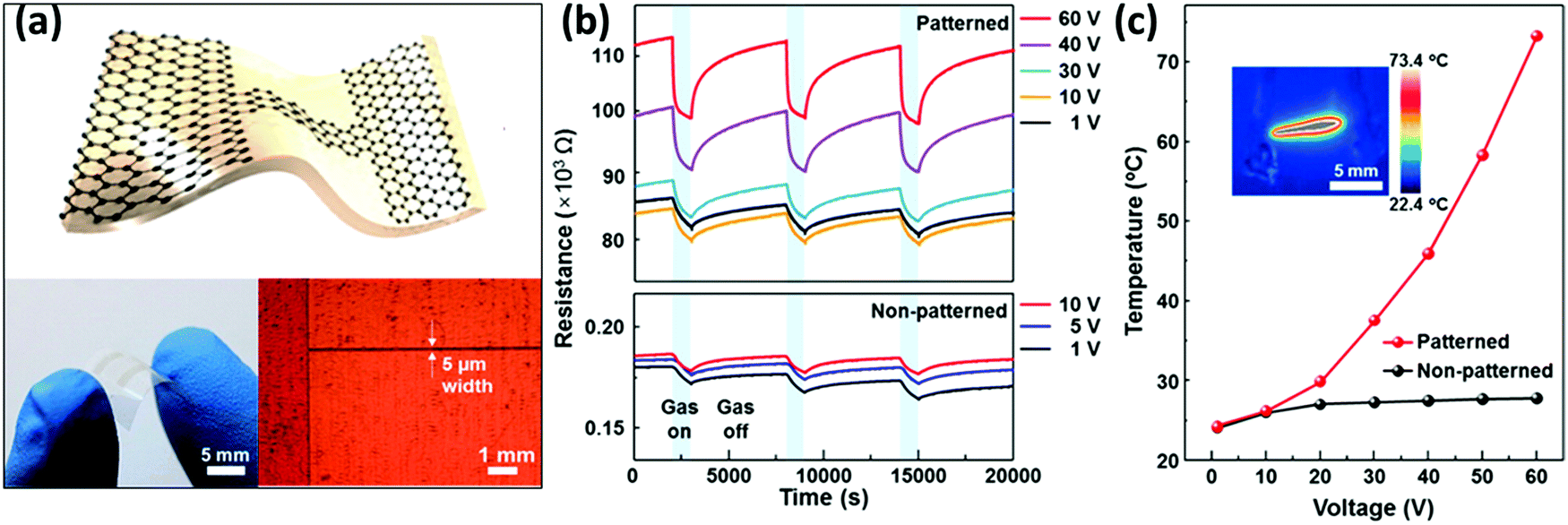 | ||
| Fig. 3 (a) Scheme (top) and photograph (bottom left) of the all-graphene flexible, transparent gas sensor and micrograph of patterned graphene (bottom right). (b) Response curves, i.e. resistance changes, recorded in patterned and non-patterned graphene sensors when exposed to three pulses of 5 ppm of NO2. (c) Thermographic image and thermal characteristics at different bias voltages. Adapted from ref. 210 with permission from the American Chemical Society. | ||
The sensing performance can be tailored by the choice of the substrate in epitaxially grown graphene.214 In fact SiC possesses a wide number of different polymorphs, and each one of them, as well as diverse crystal faces, can have doping effects on graphene.215 As an example, Pearce et al.216 realised a NO2 sensor based on epitaxially grown SLG on the atomically flat Si face of 4H-SiC. This sensor displayed an extremely high response to 2.5 ppm of NO2 (ΔR/R0 ≈ 120%). Interestingly, the response switched from n-type to p-type upon increasing the NO2 concentration because of the intrinsic n-doped nature of graphene grown on 4H-SiC. This behaviour was also demonstrated by Nomani et al.214 In their work graphene grown on the C face of 6H-SiC and on the Si face had opposite behaviour when exposed to 18 ppm of NO2: the one grown on the C face was n-type and exhibited a 4.5% increase of the conductance, while the other was p-type and exhibited a 10% decrease of the conductance.
In order to enhance the performance of a graphene-based gas sensor, a promising solution consists of introducing defects and functional groups. In fact, the absence of dangling groups on graphene's surface renders it inert to the chemisorption of gas molecules. For example, the ozone treatment of graphene sheets is a viable approach to introduce oxygen functional groups uniformly on the surface. Such defects can act as recognition sites and promote the interaction with gaseous molecules through hydrogen bonds and van der Waals forces.217 Chung et al.208 treated CVD SLG with ozone and demonstrated that the so-treated graphene features better performances in terms of sensitivity and response time for detecting NO2 compared to pristine CVD graphene. Along the same line, Masel et al.218 proved that the CVD polycrystalline graphene was much more sensitive to various organic vapours than monocrystalline pristine graphene because of the presence of structural defects.
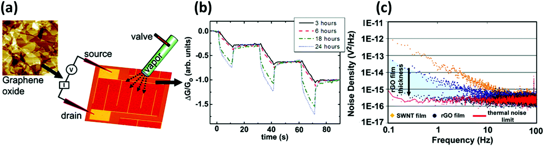 | ||
| Fig. 4 (a) AFM image of the GO film and scheme of the device. (b) Plot of the response to 5 s pulses of acetone for GO devices reduced with hydrazine for 3, 6, 18, and 24 h. (c) Noise density spectra for SWNT and rGO devices. Adapted from ref. 73 with permission from American Chemical Society. | ||
A flexible all printed gas sensor based on rGO reduced with ascorbic acid was realized by Manohar et al.224 This was done by preparing a dispersion of rGO in water in the presence of a surfactant, followed by its ink-jet printing onto a PET substrate. The device displayed a response with a detection limit in the tens of ppm range; such a response is positive, i.e. displaying increasing resistances, for NH3, dichloromethane and various alcohols, whereas it was found to provide negative response for Cl2 and NO2. Such a phenomenon has been attributed to the electron withdrawing character of Cl2 and NO2, which enhances the conductivity of semiconducting p-type rGO.212 In another case,225 a NO2 gas sensor was fabricated by reducing and patterning via laser irradiation the GO on various flexible substrates. The device exhibited a good sensitivity, which could allow the detection of 20 ppm of NO2, with complete, yet slow recovery. Another chemiresistive NO2 sensor was developed by Prezioso et al.219 using pristine GO; this device yielded the best performance when heated at 150 °C, with a response of 60% to 5 ppm of NO2, yet accompanied by the response and recovery times close to an hour. In another study226 the authors improved this GO based NO2 sensor, which reached a detection limit of just 20 ppb. Furthermore, this sensor had a response to NO2 unaffected by the humidity level and was able to detect also the presence of ethanol, acetone and ammonia. Sinitskii et al.222 fabricated a highly selective gas sensor able to discern three different alcohols such as methanol, ethanol and isopropanol with a high success rate using a 20-channel array integrated sensor of thermally reduced GO, in which each channel had a unique response due to the structural/morphological irregularity of the rGO film.
Among the various gas sensing applications, GO and rGO have been extensively used also as humidity sensors.227–230 Humidity is the presence of water vapour in air and is normally measured as relative humidity (RH), which is the ratio between the partial pressure of water and the equilibrium vapour pressure at a given temperature. It is worth reminding that having good control over the humidity in the environment is key to numerous industrial and technological processes and most importantly to ensure the comfort of human beings, improving the quality of life in living and working places.
The presence of numerous oxygen-bearing functional groups as hydroxyl, epoxy and carboxylic groups renders GO's surface highly hydrophilic, thus being a perfect candidate for sensing moisture.71 Ruoff et al.231 in 2008 demonstrated that the interaction of water molecules with these functional groups of GO determines changes in the conductivity of GO; the authors therefore concluded that highly reduced GO is not suitable for humidity sensing. Water interacts with GO mainly by increasing its conductivity because of the formation of charge carriers as hydronium and hydroxide ions as demonstrated by Yao et al. in 2012.230 In their work, GO was drop-cast on an interdigitated electrode (IDE); when a potential <2 V was applied, a 10-fold change in the GO's conductivity was observed upon varying the RH between 15 and 95%. Such a conductivity change was found to be even larger when higher potentials were applied and has been attributed to the favoured ionization of the water molecules. Similarly, Borini et al.227 spray-cast a solution of GO on top of interdigitated electrodes (IDEs) screen-printed on a flexible and transparent polyacrylonitrile (PAN) substrate. Thin films of spray-coated GO can be essentially reduced to a simple resistor–capacitor (RC) equivalent circuit in which a resistor and a capacitor are in parallel. It was found that resistance displayed an impressive exponential dependence on RH, with a 10-fold decrease when increasing the RH from 40 to 70% (Fig. 5a). Furthermore, this device showed an ultra-fast response and recovery to pulses of humid air of just 20 ms (Fig. 5b). Another GO based flexible humidity sensor was prepared by Guo et al.220via spin-coating on PET substrates. The GO film was micro-patterned using two-beam-laser interference to create alternating lines of GO and rGO. By tuning the laser power, it was possible to control the conductivity as well as the response/recovery time. The best results were obtained at 0.2 W laser power, with response and recovery times of a few seconds and a change in the resistance of 1 order of magnitude between 11 and 95% RH. In a very recent study, Tai et al.229 underlined the effect of the degree of reduction on the humidity sensing properties of GO. While GO showed a decrease in the resistance for increasing humidity, rGO displayed the opposite behaviour. By annealing GO at 150 °C for different times, integrating the so-obtained material into humidity sensors, and studying them with electrochemical impedance spectroscopy (EIS), they concluded that the resulting resistance of a macroscopic film of GO is essentially composed of two resistances in series: an intrinsic resistance within the flake (Rint) and a junction resistance between flakes (Rjunct). Both these terms are humidity dependent; in particular, the first can be expressed as two resistors in parallel – the in-plate resistance dependent only on the reduction grade and the ionic resistance, which decreases with increasing humidity. The second term (Rjunct) can also be expressed as two elements in parallel, a capacitor (CEDL) and a resistor (ROhm-contact), both humidity dependent: when the humidity increases and the GO film adsorbs water molecules, the distance between flakes increases, thus yielding an increase in both the CEDL and ROhm-contact values. As a result, with increase of humidity, Rint decreases (negative response) and Rjunct increases (positive response). For GO Rint is greater than Rjunct, thus leading to a negative response to the increased humidity, while for rGO Rint < Rjunct, thus yielding a positive response to the increased humidity (Fig. 5d).
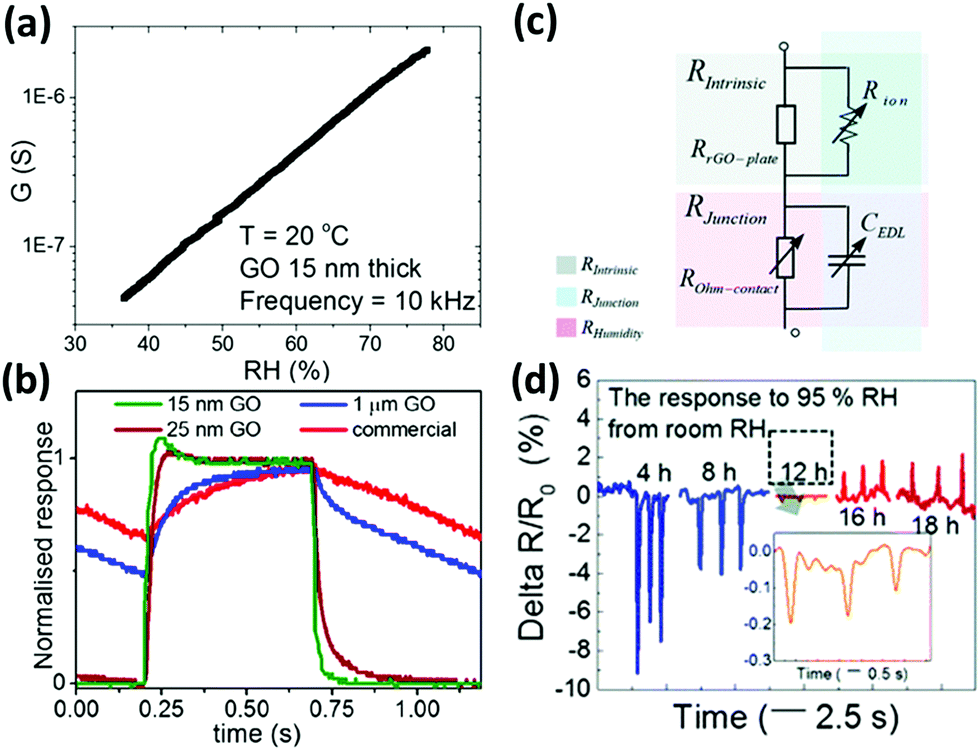 | ||
| Fig. 5 (a) Conductance dependence of an ultrathin GO film to the RH of the environment. (b) Normalized responses of the different sensors to a modulated humid air flow at 1 Hz. Adapted from ref. 227 with permission of American Chemical Society. (c) Equivalent electrical circuitry model of rGO representing intrinsic and junction-dependent resistances. (d) Responses of rGO films with different thermal reduction times to humidity pulses. Adapted from ref. 229 with permission from the Royal Society of Chemistry. | ||
In order to target more specific types of gases, GO and rGO have been functionalized with (macro)molecules bearing specific functional groups acting as selective active sites. The molecules can be chemisorbed on the surface of graphene or physisorbed on its surface. For example, Al-Mashat et al.232 reported a hydrogen sensor based on an assembly of polyaniline (PANI) adsorbed on the rGO surface. The material was synthetized via ultrasonication of an alcoholic mixture of rGO, aniline and the polymerization initiators, which promoted the polymerization of PANI selectively on the rGO surface. Then, the mixture was spray coated on a quartz substrate with a gold IDE. This functionalized rGO showed a better sensitivity to H2 compared to pure rGO and PANI with a 16.6% response to 1% H2 gas. The improved sensitivity was attributed to the higher porosity of the hybrid structure with respect to the bare PANI. In another case, a PANI–rGO assembly was used for NH3 sensing.233 Shi et al.234 fabricated a NO2 chemiresistive-type gas sensor based on sulfonated rGO (S-rGO) and rGO functionalized with ethylenediamine (EDA–rGO). In particular, S-rGO displayed a response to NO2 10 times greater than rGO and 3 times larger than EDA–rGO. Furthermore, the S-rGO also exhibited faster response and recovery and good selectivity towards NO2. The superior sensitivity of the S-rGO sensors can be attributed to the electron withdrawing characteristics of sulfophenyl groups, which enhance the hole doping in p-type rGO. After the absorption of NO2 the p-doping is further boosted, thus harnessing the material's conductivity. Hu et al.223 developed a DMMP sensor based on rGO functionalized with p-phenylenediamine, which was deposited from solution on an IDE. The response of this device to DMMP vapours was much higher than that of hydrazine reduced GO (ΔR/R0 to 30 ppm of DMMP = 11% for f-rGO and 1.5% for rGO); however, the response and recovery times were on the scale of several minutes. The chemical functionalization of GO can be used to build sensor arrays in order to recognize different gases. In a very recent study Jelinek et al.200 assembled a capacitive-type porous graphene oxide (pGO) vapour sensor in which the GO was deposited on an IDE through a freeze-drying technique in order to maximize the area exposed to the gas. In parallel, the GO was also chemically functionalized with aniline (phenyl-GO), dodecylamine (dodecyl-GO) and ethanolamine (ethanol-GO) by exploiting the amidation reaction between the amines and the carboxylic groups present on the GO surface – yet, the functionalization of epoxy groups may also occur. These three differently functionalized GOs were deposited on an IDE similarly to pGO, and by combining them in an array, it was possible to selectively detect the presence of water, NH3, toluene, EtOH, phenol and cyclohexane (Fig. 6). Additionally, the sensitivities of these devices towards the target gases were high, with high reproducibility and both response and recovery times on the time scale of few seconds.
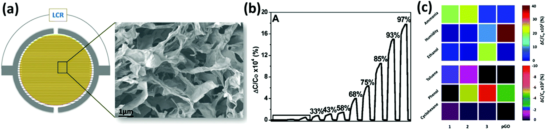 | ||
| Fig. 6 (a) Schematic structure of the device and a SEM image of the p-GO. (b) Response of the p-GO device to different values of humidity (RH%). (c) Array-based colour code identification of different vapours (180 ppm) using the functionalized pGO capacitive sensor: phenyl-GO (1); dodecyl-GO (2); and ethanol-GO (3). The colours indicated in the diagram correspond to the percentage capacitance response, according to the colour keys shown on the right. Adapted from ref. 200 with permission from Royal Society of Chemistry. | ||
The doping of GO and rGO has also been used to improve the performance of humidity sensors. Rathi and Pal228 demonstrated that GO doped with Li and B have higher sensitivity to humidity compared to GO. The Li–GO and B–GO were prepared through reaction of GO with LiOH and boric acid, then these doped GO water solutions were drop-cast on a glass with two copper electrodes on top. The Li doped GO in particular showed a response to humidity 4 times higher than un-doped GO. Also in this case the higher performances can be attributed to the increased p-doping of Li–GO.
For example, it is well-known that metals such as palladium and platinum exhibit a catalytic activity towards the adsorption of hydrogen.236 With this in mind, palladium– and platinum–graphene composites have been extensively explored to target H2 gas;182,235,237–241 hydrogen is colourless and odourless but when mixed with air forms an explosive mixture; thus, its detection is of paramount importance for safety. Kaniyoor et al.235 produced a hydrogen sensor based on GO decorated with Pt NPs: the Pt NPs were grown in situ on the GO surface and then the so decorated GO was drop-cast on an alumina substrate with pre-patterned Cu electrodes. This device showed a 16% increased electrical resistance when exposed to 4% H2 yet accompanied by a slow responsivity. Similarly, Wu et al.237 fabricated a H2 sensor based on a Pd thin film (1 nm) evaporated over CVD graphene with 12% sensitivity towards the exposure to 1% H2. Chung et al.238 realized a flexible hydrogen sensor composed of CVD graphene decorated with Pd NPs, exhibiting an impressive sensitivity of 30% to 1% H2. Reduced GO decorated with Pd NPs has also been used to sense NO gas for medical applications by Li et al.185 The rGO with physically absorbed Pd NPs on its surface was deposited on CVD graphene-coated Ni electrodes (Fig. 7a). This device exhibited high sensitivity with an impressive limit of detection of 2 ppb, which is notably higher than that of the reference device assembled without decorated rGO or without graphene-coated electrodes (Fig. 7b). In this case, Pd NPs may act as absorption sites of NO molecules, promoting the donation of electrons from NO to rGO. Furthermore, the interaction of the hybrid with NO can lower the Schottky barriers between rGO and Pd NPs, leading to a further increase in the conductance.
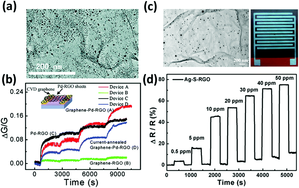 | ||
| Fig. 7 (a) Transmission electron microscopy (TEM) image of Pd–rGO sheets. (b) Relative changes in the conductances of the various devices versus time when exposed to 1, 10, 60, and 120 s pulses of NO gas. Inset: Scheme of the device. Adapted from ref. 185 with permission from American Chemical Society. (c) TEM image of Ag–S–rGO and photograph of the sensing device printed on PI. (d) Response of the Ag–S–rGO sensor as a function of time in various concentrations of NO2 gas. Adapted from ref. 242 with permission from American Chemical Society. | ||
Interestingly, the modification of rGO with functional groups capable of boosting the p-doping can be combined with the catalytic activity of metal NPs. For example, Huang et al.242 assembled a flexible, all-printed NO2 sensor based on sulfonated rGO/Ag NPs. The rGO was first sulfonated and then Ag NPs were grown in situ on the rGO surface via hydrazine reduction of AgNO3 (Fig. 7c). Then Ag electrodes and the rGO/Ag NP based ink were printed on a PI substrate. This sensor displayed a 74.6% fast response to 50 ppm of NO2. Besides, the sensor was quite robust: it exhibited good stability over time and tolerance to humidity (Fig. 7d). The sensor could also detect NH3, with a similar, yet negative response.
Hybrid materials composed of graphene and metal oxide nanostructures184,243–249 or quantum dots250,251 have also proved to enhance the sensing performances of graphene to NO2, ethanol, H2S and other gases. In fact, semiconducting metal oxides such as ZnO, SnO2, In2O3, and Cu2O have been already employed in gas sensing,252,253 yet the high operating temperature and low conductivity represented a severe limit towards their application. Deng et al.243 synthetized hybrid rGO/Cu2O nanowire mesocrystals under hydrothermal conditions and integrated them into a NO2 gas sensor. The hybrid sensor displayed a higher sensitivity compared to those of the single components alone, with an impressive detection limit of 64 ppb (Fig. 8a and b). Also, in this case, the response resulted from the electron withdrawing effect of NO2 towards the p-type rGO and Cu2O semiconducting mesocrystals, and it took further advantage of the higher porosity of the hybrid material. An ethanol sensor was assembled by Yi et al.244 by growing semiconductive vertically aligned ZnO nanorods on a metal bottom electrode and depositing CVD few-layer graphene on top as the top contact. This sensor, with a geometry similar to those of metal–insulator–metal devices, offered a 900% sensitivity to 10 ppm of ethanol and a good flexibility. However, an operating temperature as high as 300 °C was required to leverage the n-type characteristic of semiconductive ZnO nanorods and obtain a good sensitivity to the electron donor EtOH. In another study245 GO decorated with ZnO NPs was used to sense CO and NH3 gases. ZnO NPs were grown in solution on the GO surface; such a decorated GO was spin-coated on ITO patterned glass substrates. This device, when operated at room temperature, revealed a much higher sensitivity towards CO and NH3 compared with the two components alone. In particular, the change in conductivity was ∼24% to 1 ppm of NH3 and 22 ppm of CO. Similarly, Cuong et al.246 reported a H2S sensor based on vertically aligned ZnO nanorods hydrothermally grown on the surface of spray-coated rGO, which showed high sensitivity in oxygen, but long response and recovery times. Another H2S sensor was developed by Zhou et al.247 by hydrothermally growing Cu2O nanocrystals on a GO surface and drop-casting the suspension onto a gold IDE on a Si/SiO2 substrate. The GO/Cu2O assembly was demonstrated to have better performances compared to the isolated components, with a high 11% sensitivity to 5 ppb of H2S at room temperature and response and recovery times on the few minutes time scale. rGO/In2O3 assemblies have been used to detect NO2249,254 for environmental monitoring. Feng et al.254 were able to embed In2O3 nanocubes in rGO networks using InN NWs and GO as precursors. Depending on the ratio between the two components, different morphologies were obtained: the best sensing performances were found when a 1![[thin space (1/6-em)]](https://www.rsc.org/images/entities/char_2009.gif) :1 InN:GO ratio was used (Fig. 8c). Such a sensor exhibited a 61% change in the resistance when exposed to 5 ppm of NO2 and a markedly high selectivity towards interfering gases (Fig. 8d). In 2017 Liu et al.249 overtook these performances by combining flower-shaped In2O3 nanocrystals with rGO, thereby obtaining a sensor with an impressive 3 orders of magnitude increase in the resistance when exposed to 1 ppm of NO2 combined with a detection limit lower than 10 ppb.
:1 InN:GO ratio was used (Fig. 8c). Such a sensor exhibited a 61% change in the resistance when exposed to 5 ppm of NO2 and a markedly high selectivity towards interfering gases (Fig. 8d). In 2017 Liu et al.249 overtook these performances by combining flower-shaped In2O3 nanocrystals with rGO, thereby obtaining a sensor with an impressive 3 orders of magnitude increase in the resistance when exposed to 1 ppm of NO2 combined with a detection limit lower than 10 ppb.
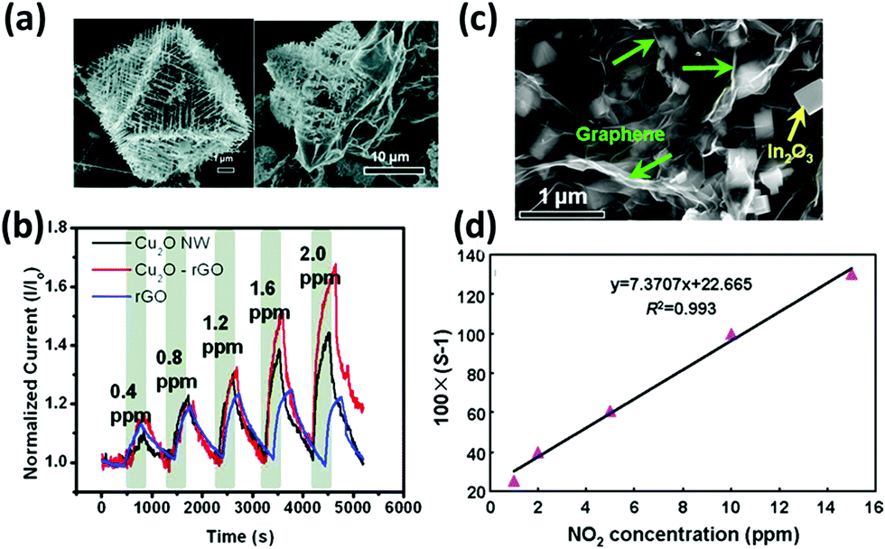 | ||
| Fig. 8 (a) SEM images of rGO–Cu2O mesocrystal composites, and (b) dynamic responses of Cu2O NW, rGO–Cu2O, and rGO devices under increasing NO2 exposure. Adapted from ref. 243 with permission from American Chemical Society. (c) SEM image of the In2O3 cubes/rGO composites at a 1:1 mass ratio. (d) Linear fitting curve of the sensor response versus NO2 concentration. Adapted from ref. 254 with permission from American Chemical Society. | ||
The sensing of simple alkanes, such as methane and ethane, is important because of the industrial relevance of these molecules. However, very few examples of sensing of these gases can be found in the literature because of the weak doping nature of these apolar molecules.255–257 For example, a hydrogen and liquid petroleum gas (LPG) sensor based on rGO decorated with SnO2 quantum dots was developed by Lee et al.,251 showing an impressive response of 89% to 500 ppm of H2 and 92% to 500 ppm of LPG. Zhang et al.255 produced a methane sensor based on a nanocomposite of rGO and ZnO nanocrystals that displayed a decent and fast response to 100 ppm of CH4 and a good selectivity towards interfering gases; unfortunately, a high operating temperature of 190 °C is necessary for proper functioning of this sensor.
Polymers and semiconducting polymers coupled with graphene, GO and rGO constitute the third large family of hybrid assemblies. Some of these assemblies with conducting polymers, like the polyaniline/GO assembly, have already been discussed in the previous paragraph232 as the boundary between polymer functionalized GO/rGO and polymer–GO/rGO assemblies is blurred. In a typical example, in 2014 Zhang et al.221 developed a resistive-type, flexible humidity sensor based on the assembly of GO and a polyelectrolyte, i.e. poly(diallyldimethyammonium chloride) (PDDA), using the layer-by-layer (LbL) deposition method. The nanostructured film was fabricated on a Cu/Ni IDE on a PI substrate. In the first instance, a bi-layer of PDDA and an ionic polymer was self-assembled on the substrate as precursor layers for charge enhancement, and then 5 GO/PDDA layers were deposited by alternating immersions into PDDA and GO suspensions for five repetitive cycles. Following that, the GO was chemically reduced by soaking the film in a solution of HBr acid. Such an assembled device exhibited a 37% increase in the resistance when passing from 0% RH to 97% RH, with response and recovery times of a few minutes, an excellent linearity of the response and long-term stability over time. The superior sensor performances were attributed to the high surface area of the assembly, the p-type semiconducting properties of rGO at low RH, and the interlayer swelling of the PDDA/RGO film at high RH, which contributes to the resistance increase. In another study Shi et al.258 synthetized GO/conducting polymer composite hydrogels, including GO/polypyrrole (PPy) and GO/PANI, by chemical polymerization in situ of the corresponding monomers in aqueous dispersions of GO, where GO sheets acted as 2D templates. These gels showed many interesting properties, including electrical conductivity and electrochemical activity. In particular, the GO/PPy gel, once lyophilized, exhibited a good sensitivity to NH3 gas. In this case, the improved response was attributed to the high surface area of the conductive gel compared to that of the bare polymer film.
A nanocomposite thin film of chemically exfoliated graphene and PANI was used by Wu et al.257 to sense methane at room temperature, with a decent 10% response to 10 ppm of gas. Shi et al.259 prepared a highly sensitive NO2 sensor based on electrospun PVA/PEI nanofibers coated with a thin GO layer, which self-assembled on the surfaces of the nanofibers for charge interaction. The nanofibers were deposited on an IDE and then exposed to hydrazine vapours to reduce the GO. This sensor displayed an impressive sensitivity, with a 16% response to 150 ppb of NO2 and good linearity until 1 ppm; furthermore, the stability and the selectivity towards NO2 were high, and the response and recovery times were around 5 minutes.
The combination of graphene with ionic liquids is a similar route to achieve high sensitivity and selectivity in gas sensing. Within this framework, Ariga et al.260 developed a sensor capable of discriminating between various organic vapours based on a multi-layered rGO/ionic liquid film assembled in solution via the LbL method on a quartz microbalance. Assemblies of CNTs and graphene have also been employed for gas sensing. In 2010 Jeong et al.261 produced a flexible NO2 sensor using a CNTs/rGO hybrid film. A rGO film was deposited on a plastic substrate with a gold IDE followed by the CVD deposition of vertically aligned CNTs on top. The so-fabricated sensor revealed a sensitivity of 20% after 60 min exposure to 10 ppm of NO2 at room temperature.
The most important performance parameters of all the graphene based gas sensors described in this section, including the response time and the sensitivity (calculated as the ratio between the response % and the corresponding gas concentration expressed in ppm), are summarized in Table 1.
| Material | Sensed gases | Response/recovery time | Limit of detection | Sensitivity (response × ppm−1) | Ref. |
|---|---|---|---|---|---|
| List of abbreviations. SLG: single layer graphene, ME: mechanically exfoliated, BLG: bi-layer graphene, CVD: chemical vapour deposition, GO: graphene oxide, rGO: reduced graphene oxide, CHCl3: chloroform, THF: tetrahydrofuran, MeOH: methanol, MeCN: acetonitrile, DMMP: dimethyl methylphosphonate, HCN: hydrogen cyanide, EDA: ethylenediamine, PANI: polyaniline, PDDA: poly(diallyldimethyammonium chloride), LbL: layer-by-layer, PVA: polyvinyl alcohol, PEI: polyethylenimine, CNTs: carbon nanotubes, NPs: nanoparticles, Nrods: nanorods, NCryst: nanocrystals. | |||||
| SLG (ME) | NO2 | 500 s | ppb | 4% | 201 |
| H2O, nonanal, octanoic acid | 0.5 ppm | 0.6–1% | 204 | ||
| CO2 | 10 min/10 min | 0.26% | 206 | ||
| NO2 | 4 min/4 min | 100 ppm | 0.08% | 80 | |
| SLG/BLG (ME) | THF, MeOH, MeCN, CHCl3 | 205 | |||
| SLG (CVD) | CH4, NH3, H2 | 9 min/9 min | 0.046% (NH3) | 211 | |
| SLG/BLG (CVD) | NO2 | 95 s/11 s | 0.98% | 209 | |
| SLG (CVD) oxidized with O3 | NO2 | 15 min/30 min | 0.0085% | 208 | |
| SLG (CVD) patterned | NO2, NH3 | 89 s/579 s | 2.6% (NO2) | 210 | |
| CVD graphene foam | NH3 | 800 s/1200 s | 0.03% | 212 | |
| SLG (epitaxially grown) | NO2 | 1 h/3 h | 48% | 216 | |
| NO2 | 250 s/150 s at 300 °C | 0.55% | 214 | ||
| GO | H2O | 20 ms/20 ms | 30%/RH | 227 | |
| NO2, H2O | 40 min/40 min | 12% | 219 | ||
| NO2 | 40 min/40 min | 20 ppb | 250% | 226 | |
| H2O | 12.5% | 230 | |||
| rGO | Acetone, DMMP, HCN | 5 s | 100% | 73 | |
| NO2, Cl2, NH3 | 10 min/10 min | 0.25% (NH3) | 224 | ||
| H2O | 231 | ||||
| NO2 | 10 min/30 min | 0.05% | 225 | ||
| H2O | 20 s/30 s | 10.7%/RH | 148 | ||
| Li and B doped GO | H2O | 4 s | 35.3% | 228 | |
| Sulfonated-GO and EDA–GO | NO2 | 50% | 234 | ||
| Phenyl-GO, dodecyl-GO; ethanol-GO | Various gases | 15 s/10 s | 200% (NH3) | 200 | |
| p-Phenylenediamine/GO | DMMP | 1080 s/360 s | 0.4% | 223 | |
| PANI/rGO | H2 | 2 min/3 min | 0.0016% | 232 | |
| PANI/graphene flakes | CH4 | 1 min/1 min | 10 ppm | 2.5% | 257 |
| PDDA/GO LbL assembly | H2O | 2 min/3 min | 0.38%/RH | 221 | |
| Microfiber PVA–PEI/rGO | NO2 | 4 min/10 min | 110% | 259 | |
| CNTs/GO | NO2 | 1 h/3 h | 0.5 ppm | 2% | 261 |
| Ag NPs/sulfonated-GO | NO2, NH3 | 12 s/20 s | 1.49% (NO2) | 242 | |
| Pd film/CVD SLG | H2 | >10 min | 0.0012% | 237 | |
| Pd NPs/CVD SLG | H2 | 15 min/20 min | 0.003% | 238 | |
| Pd/rGO | NO | 265 s | 35% | 185 | |
| Pt NPs/GO | H2 | 9 min/20 min | 0.004% | 235 | |
| Cu2O NPs/rGO | H2S | 5 min/5 min | 2200% | 247 | |
| Cu2O/rGO | N2O | 5 min/10 min | 34% | 243 | |
| In2O3/rGO | NO2 | 4 min/1 min | 109800% |
249 | |
| In2O3/rGO | NO2 | 3 min/4 min | 12.2% | 254 | |
| ZnO NPs/rGO | CO, NH3 | 5 min | 24% (NH3) | 245 | |
| ZnO Nrods/rGO | H2S | >30 min | 246 | ||
| ZnO Nrods/CVD SLG | EtOH | 90% | 244 | ||
| ZnO NCryst/rGO | CH4 | 1 min/10 s | 100 ppm | 0.05% | 255 |
2.2 Gas sensing with transition metal dichalcogenides
The sensing properties of TMDs are based on the already discussed charge-transfer mechanism. Yue et al.191 gained deep insight into such a mechanism by focusing on n-type MoS2 as an exemplary system. In this article, the charge transfer mechanism between different gas molecules including O2, H2O, NH3, NO, NO2, CO, etc., and monolayer MoS2 was explained with the aid of DFT calculations. The authors showed that the conduction band (CB) of pristine n-type MoS2 monolayers is already populated by some electrons at room temperature. When the monolayer is exposed to electron–acceptor gases such as O2, H2O, NO, NO2, and CO, electrons are transferred from MoS2 to the sensitive gases, leading to a decrease of carrier density in MoS2, which ultimately yields an increased resistance. In contrast, NH3, which behaves as an electron-donor, transfers electrons to the MoS2 monolayer, thereby reducing its resistance.The charge transfer between TMD monolayers and gases can also be evidenced by changes in the photoluminescence (PL), which is due to the direct band gap properties of TMD monolayers. Tongay et al.262 showed that the light emission efficiency of these TMDs can be modulated by physisorption of gas molecules such as O2 and H2O, as a result of a molecular gating effect. The charge depletion in n-type materials such as MoS2 and MoSe2 caused by the charge transfer to molecules such as O2 and H2O leads to a drastic enhancement in photoluminescence for the stabilization of neutral excitons X0.
Among the various TMDs, MoS2 is the most studied material. Mechanically exfoliated MoS2 has been successfully used to detect a wide range of gases.14,190,193,263 For instance, Zhang et al.190 fabricated miniaturized FETs based on mechanically exfoliated MoS2 for the detection of NO. Single, bi-, tri- and quadri-layers of MoS2 transferred onto Si/SiO2 substrates were investigated in this work. The sensitivities of these devices to NO were high and the responses were fast; however, the current passing through a single-layer thick MoS2 FET was unstable, while the devices based on 2-, 3- and 4-layer MoS2 showed both high sensitivity and stability with a detection limit of 0.8ppm of NO. In a similar study Late et al.14 prepared transistors by depositing mechanically exfoliated MoS2 flakes on Si/SiO2 substrates and contacting them with gold top electrodes through electron beam lithography, and they employed them to sense NO2, NH3 and humidity (Fig. 9a). From the analysis of flakes consisting of 1, 2 and 5-layers it was observed that the signal was unstable for monolayers, while among 2 and 5-layers the latter exhibited the highest response to the sensed gases. As expected from the charge transfer mechanism, NO2 produced a negative resistance response, while NH3 had the opposite behaviour (Fig. 9b and c). For the same reason, the applied gate voltage had opposite effects in NH3 and NO2 in increasing or decreasing the sensitivity, and these effects were larger for the 5-layer device. In addition, the effects of green light irradiation on the sensitivity and response time of the device were also explored. The reason for the increased and stable response in the devices based on few-layers compared to the single-layer thick device remains unclear, yet the authors showed with DFT calculations that the adsorption of NO2 was slightly favoured in the few-layer thick devices. In another example Perkins et al.193 measured the conductance changes in a device based on mechanically exfoliated MoS2 after exposing it to various organic vapours. They found that the device had high selectivity towards triethylamine (TEA) and acetone with a detection limit of 1 ppm over the last analyte.
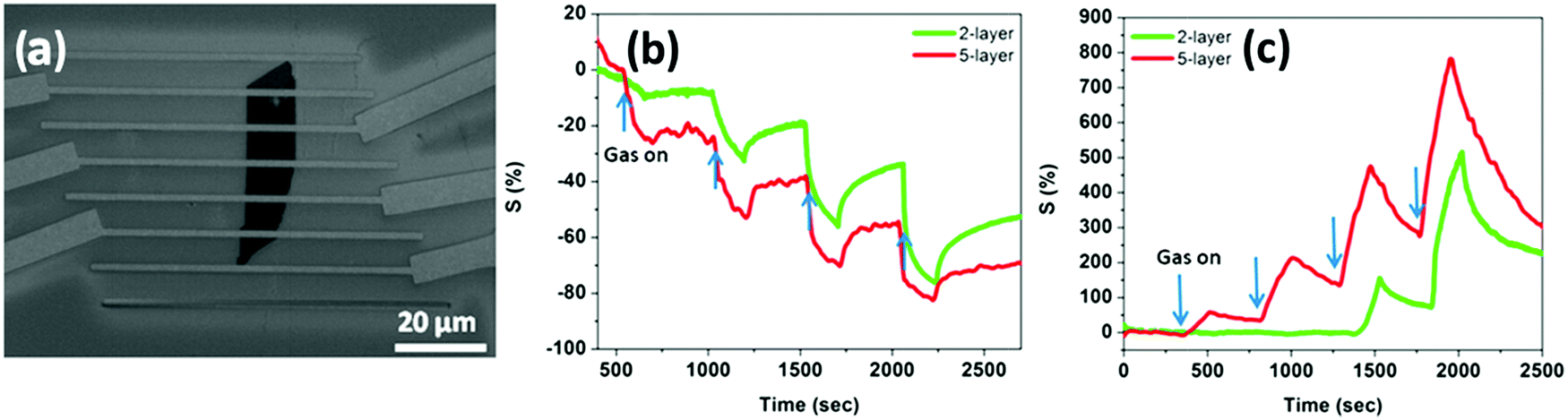 | ||
| Fig. 9 (a) SEM image of a two-layer MoS2 transistor device. Sensing performances of the 2 and 5-layer devices when exposed to 100, 200, 500, and 1000 ppm of (b) NH3 and (c) NO2. Adapted from ref. 14 with permission from the American Chemical Society. | ||
Dispersions of MoS2 sheets in solution can be obtained with a relatively high yield and low cost by liquid-phase exfoliation. These dispersions can be processed to generate films of overlapping flakes, which have been used as active materials to detect different gases.192,264,265 For example, Yao et al.265 prepared a water dispersion of MoS2 flakes combining grinding and sonication of the bulk material. The dispersion was deposited with an inject printer onto pre-patterned microelectrodes and the so-obtained device was used to detect NH3 gas up to a few ppm. A similar method that relies on the intercalation of Li ions within the MoS2 layers and their subsequent exfoliation in water solution through ultrasonication was used by Zhang et al.141 to sense NO. The dispersion of MoS2 flakes was deposited by drop-casting on a Si/SiO2 substrate pre-patterned with gold electrodes to form a thin-film transistor (TFT), which was found to be sensitive to NO at concentrations down to 0.4 ppm.
Similarly to graphene, MoS2 can also be produced by CVD.143 In 2014 Liu et al.144 fabricated FETs by contacting through EBL small triangular-shaped monolayers of MoS2 grown by CVD on Si/SiO2 substrates (Fig. 10a). These devices exhibited a high Schottky barrier (ΔSB) between the Ti/Au contacts and the monolayer, which can be modulated by exposing the devices to NO2 and NH3 gases. In particular, NO2 adsorption increases the ΔSB and thus the contact resistance, whereas NH3 adsorption decreases both of them. The effect of the Schottky barrier modulation, together with the charge transfer mechanism, yielded an increase in the sensitivity of the device to both the analytes, with changes in the conductance up to 3 orders of magnitude and detection limits down to 20 ppb of NO2 and 1 ppm of NH3 (Fig. 10b). Cho et al.146 produced a gas and photo-detector based on a wafer-scale film of 3-layer MoS2 deposited on sapphire substrates via CVD with IDE gold electrodes on top. This sensor exhibited good sensitivity and selectivity to NO2, with a response around 40% to 120 ppb combined with a stable cycling behaviour. Furthermore, the response time was fast, yet the recovery at room temperature was not complete even after 30 minutes. Similarly, a 3-layer MoS2 film produced by CVD on sapphire substrates was developed by Cho et al.266 for the sensing of NO2 and NH3. The device exhibited an increased resistance when exposed to NO2 and a decreased resistance when interacting with NH3, as expected from the charge-transfer mechanism.
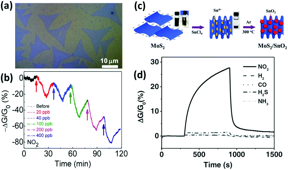 | ||
| Fig. 10 (a) Micrograph of triangular shaped CVD grown MoS2 monolayers supported on a Si/SiO2 substrate. (b) Response of the device upon exposure to increasing NO2 concentration. Adapted from ref. 144 with permission from American Chemical Society. (c) Schematic illustration of the preparation of a SnO2/MoS2 hybrid. (d) Response of the device to 10 ppm of various gases, highlighting the selectivity towards NO2, the sensitivity and the response time. Adapted from ref. 270 with permission from Wiley-VHC. | ||
The sensitivity of MoS2 to gases could be improved by increasing the number of active sites that can interact with the analyte of interest through processes of molecular absorption on sulphur vacancies and edges. For example, Jung et al.147 showed that sensors based on MoS2 layers vertically aligned, thus exposing their edges to the environment, exhibited a higher response to NO2 and EtOH gases. The films of horizontally and vertically aligned MoS2 layers were produced via CVD. By increasing the thickness of the films, the number of vertically aligned layers increased, and at a thickness of 15 nm almost all the surface was covered by vertically aligned layers, as revealed by TEM mapping. These films exhibited a response 5 times greater than the 1 nm thick film, because of the increased edge sites exposed to the environment.
The surface functionalization of MoS2 with molecules or nanomaterials as metal and metal oxide NPs represents an alternative viable method to increase the interactions with the gas molecules, and thus to harness the device sensitivity.267,268 For example, Zhang et al.267 fabricated a flexible TFT depositing a film of MoS2 obtained with a method previously described141 on a rGO electrode array on polyethylene terephthalate (PET). Successively, Pt NPs were deposited on the surface of the MoS2 film and the device was employed to detect NO2. The device functionalized with the Pt NPs showed a response to NO2 3 times faster than the non-functionalized device, with detection limits as low as 2 ppb. The reason for such an improved sensitivity was attributed to the formation of a Schottky barrier between the MoS2 and the Pt NPs. In a similar study Sarkar and co-workers269 functionalized MoS2 with various metallic NPs, including Ag, Pd, Pt, Sc and Y, and examined their doping effects. The Pt NPs functionalized MoS2 device revealed an improved sensitivity to H2 gas compared to the pristine MoS2 device. A H2 sensor based on Pd NPs functionalized MoS2 was also assembled by Jin et al.268 by drop-casting a water suspension of MoS2 flakes obtained by liquid-phase exfoliation and Pd NPs. This sensor displayed a fast response and good recovery upon exposure to H2 (0.5–5%) and a decent cross-sensitivity. Metal oxide NPs have also been used to improve the sensitivity; in particular, semiconducting SnO2 has been employed to sense humidity,198 NO2270 and EtOH.271 For example, Chen et al.270 prepared a NO2 sensor based on SnO2 nanocrystal decorated MoS2 nanosheets. The material was prepared as depicted in Fig. 10c. A MoS2 flake suspension was produced by lithiation of MoS2 followed by liquid exfoliation, then SnCl was added to the suspension and Sn4+ ions got absorbed on the negatively charged flakes’ surfaces. Finally, the SnO2/MoS2 hybrid was obtained by annealing the filtered suspension at 300 °C in argon. Interestingly, this material showed p-type behaviour because of the p-doping effect of the SnO2 nanocrystals. The sensor based on the hybrid showed a decent sensitivity to NO2, with a 30% response to 10 ppm and a detection limit of 0.5 ppm combined with good reversibility and selectivity (Fig. 10d).
MoS2 can also be functionalized with dangling molecules, especially through the covalent attachment of thiolated molecules on the sulphur vacancies of the MoS2 surface.272 By applying such a strategy, Jung et al.13 developed a volatile organic compound (VOC) sensor for breath analysis based on MoS2 nanosheets obtained via liquid-exfoliation functionalized with mercaptoundecanoic acid (MUA). This sensor exhibited a good sensitivity down to 1 ppm to various VOCs including toluene, hexane, acetone, propanal and ethanol. Furthermore, while the resistance of a pristine MoS2 based device increased upon exposure to all the sensed gases, the MUA–MoS2 sensor once exposed to the molecules with oxygen functionalities displayed a decrease in the resistance. These differences originated from the diverse interaction of the oxygen containing molecules with the dangling MUA. In particular, the oxygen-bearing gas molecules can interact via hydrogen bonding with the exposed carboxyl group in MUA and then form an electron-rich region able to transfer the charge to the MoS2 sensing channel.
Among the other TMDs, MoSe2, WS2, WSe2, ReS2 and PtSe2 have also been employed for fabricating gas sensing devices by exploiting their diverse semiconducting characteristics and their unique high surface area-to-volume ratios. For example, MoSe2 has found application as an NH3 sensor in a study of Late et al.273 The device was based on a single-layer MoSe2 flake obtained via mechanical exfoliation deposited on a Si/SiO2 substrate and contacted with gold electrodes by EBL. The device showed a sensitivity to NH3 in concentration from 50 to 500 ppm and a response time of 2.5 min. The doping effect of NH3 was also confirmed by the shift in the Raman spectrum after the absorption of NH3.
WS2 has been used in recent years as a sensor for NH3,52,194 humidity195,274 and alcohols.52,195 Li et al.52 developed a transistor based on a mechanically exfoliated multilayer WS2 flake and measured the current change and the photoresponse of the transistor when exposed to different gases including NH3, ethanol and O2. In particular, NH3 and ethanol behaved as electron-donors, yielding an increase in current and photo-responsivity in the n-type WS2 device, while O2 extracted electrons from the device, resulting in a current decrease and a lower photo-response. The device showed the highest sensitivity toward NH3 and really fast response and recovery to all the sensed gases. Pumera et al.195 prepared a chemiresistive device depositing metallic 1T-WS2 flakes obtained through liquid exfoliation on an IDE. The selective vapour sensing capabilities of the device were studied with impedance spectroscopy. When exposed to methanol, the device presented an impedance phase spectrum with a resonant frequency maximum around 1 Hz, while with water the maximum shifted to 1 kHz. Therefore, the device was able to discern methanol and water isolated and mixed together by simply selecting specific frequencies, even when high concentrations of interfering gases were present. Duesberg et al.194 reported an NH3 sensor based on CVD WS2 thin films. The films with thicknesses ranging from 1 to 50 nm were grown on Si/SiO2 substrates with gold IDEs using H2S plasma to sulphurise WO3 films at 500 °C. The so-achieved devices demonstrated good sensitivity to NH3, with a detection limit of 1.4 ppm.
WSe2 is another TMD semiconductor which has been used to detect toxic gases. Javey et al.275 assembled a p-type FET based on mechanically exfoliated WSe2 monolayers for NO2 detection. A high work function metal such as Pd was used as source and drain electrodes to lower the contact resistance for hole injection. Upon exposure to 0.05% of NO2 the source–drain current increased 5 orders of magnitude as a result of the decrease of the Schottky barrier and increase of p-doping. Furthermore, in devices with a top-contact gate the on–off ratio was also greatly improved after NO2 exposure.
Recently, ReS2, ReSe2 and PtSe2 have also been employed for gas sensing.276–279 Yang et al. reported the photoresponse of monolayer ReS2276 and ReSe2278 based FETs under red light illumination in NH3 and O2 gases. The increase in current that was observed under illumination was higher in an NH3 atmosphere for ReS2, while for ReSe2 it was higher in an O2 atmosphere. With the aid of DFT spin-polarized calculations, the reason for the different photoresponse behaviours of single-layer ReS2 and ReSe2 FETs in O2 and NH3 was attributed to the different transfer directions and quantities of electrons in n-type ReS2 and p-type ReSe2. Yim et al.279 prepared a FET by depositing a thin layer PtSe2 film by CVD on a Si/SiO2 substrate and tested it as a photodetector and gas sensor. The FET exhibited a fast detection of NO2, with a resistance decrease of 0.25% to 1 ppm of gas and response and recovery times of 30 and 10 s respectively.
2.3 Gas sensing with other 2DMs
SnS2 is a layered material similar to TMDs exhibiting a higher electronegativity, which can potentially enhance the gas sensing capabilities. Ou et al.280 developed a sensitive and selective NO2 sensor based on few-layer SnS2 flakes obtained by a wet chemical synthesis technique. The flakes, with lateral sizes ranging between 80 and 200 nm, were synthetized from a solution of SnCl4 and sulphur and then drop-cast on an IDE. The device displayed a linear response from 0.6 to 10 ppm of NO2, with an extremely high sensitivity of 3500% to 10 ppm of NO2 and response and recovery times of 170 and 140 s, respectively, at an operating temperature of 120 °C. Furthermore, the device showed high selectivity to NO2 among high concentrations of various interfering gases; these results were attributed to the strong affinity of SnS2 for NO2 as well as the favourable Fermi level of SnS2 to the energy of the partially occupied NO2 molecular orbitals.In another example, Shi et al.281 developed an NH3 sensor operating at room temperature based on flower-shaped nanoflakes of SnS2 prepared by a solution method. The sensing device was produced depositing a paste made of the interconnected flakes on an IDE. The sensor, when exposed to concentrations of NH3 ranging between 5 and 150 ppm, presented a 21% sensitivity to 5 ppm of gas with response and recovery times of 40 and 100 s, respectively. Another NH3 sensor based on SnO2/SnS2 hybrid flakes was fabricated more recently by Xu et al.197 To form the hybrid structure, SnS2 flakes were first produced by a solution method and deposited on a gold IDE, then the device was heated to 300 °C in air in order to partially oxidise the surface to SnO2. This device showed good sensitivity to NH3, with a 16% response to 10 ppm of NH3, which was much higher compared to the sample with non-oxidized SnS2 or with the completely oxidized SnO2. The device also exhibited a good dynamic range from 10 to 500 ppm of NH3, high reproducibility and a response time of just 11 s.
Black phosphorus is a promising candidate as a platform for gas sensing for its electrical properties and its sensitivity to the environment, which is usually considered as a drawback.153 First-principles calculations159 made it possible to shed light on the interaction of many gases with phosphorene. The gas molecules can get physisorbed on the phosphorene surface and interact via van der Waals forces, yielding a modification of the electronic properties of phosphorene. O2, NO2 and NO act as strong electron acceptors, whereas CO, H2, H2O and NH3 act as electron donors. Abbas et al. first reported on the chemical sensing of NO2 using a FET based on mechanically exfoliated multilayer phosphorene.158 The FET was produced by exfoliating the black phosphorus with the Scotch-tape method on a Si/SiO2 substrate and patterning gold electrodes by EBL. The sensor displayed increased conductivity upon NO2 exposure with a 3% response to 5 ppb of the gas. Moreover, when the device was exposed to NO2 concentration ranging from 5 to 40 ppb, its response complied with the Langmuir isotherm for molecules adsorbed on a surface, confirming the charge transfer as a sensing mechanism. Cui et al.96 reported a similar FET based on phosphorene nanosheets exfoliated with the Scotch-tape method for NO2 sensing. The sensor showed thickness dependent performance with sensitivities up to 190% to 20 ppb of NO2, excellent stability and high selectivity in the presence of interfering gases.
Phosphorene also demonstrated good sensitivity to organic vapors160 and humidity.282 Pumera et al.160 developed a highly selective methanol sensor based on black phosphorus plates deposited on a gold IDE. The device was studied with EIS: when exposed to methanol, a strong signal at a resonance frequency of 1 kHz appeared in the impedance phase spectrum and its intensity was proportional to the methanol concentration in the 380–1900 ppm range. High reproducibility, long-term stability and excellent selectivity in the presence of interfering gases were also established. Yasaei et al.282 explored the possibility of employing of phosphorene films as humidity sensors. Phosphorene flakes were produced by ultrasonication in liquid and then filtered to obtain thick films of stacked flakes that were used as chemiresistors. When the humidity was increased from 10 to 85% RH, the conductivity increased by 4 orders of magnitude. From EIS measurements, a sensing mechanism based on the formation of ionic charge carriers caused by ionization of the water molecules and solvation of the phosphorus oxoacids was hypothesized.
Hexagonal boron nitride also exhibits promising properties, which make it an interesting material for gas sensing as was assessed in few first-principles calculations.283,284 However, the only example of the application of hBN as a gas sensor was reported by Feng et al.199 In particular, an O2 and CH4 sensor based on wafer-scale hBN nanosheets (1.7 nm thick) obtained using the CO2-pulsed laser deposition technique was developed. Such a sensor revealed a sensitivity to 100ppm of O2 of 150% with response and recovery times around 70s and 100s, respectively. The sensitivity to 100ppm of CH4 was even greater (around 780% with response and recovery times reduced to 15s and 20s, respectively). The highest sensitivity towards CH4 could be caused by the higher polarizability compared to O2, which promotes its adsorption on the surface and at grain boundaries of hBN, thereby changing its conductivity.
The properties and the performances of the gas sensing devices based on TMDs and other layered 2DMs are summarized in Table 2.
| Material | Sensed gases | Response/recovery time | Limit of detection | Sensitivity (response × ppm−1) | Ref. |
|---|---|---|---|---|---|
| List of abbreviations. ME: mechanically exfoliated, TEA: triethylamine, CVD: chemical vapour deposition, align.: aligned, EtOH: ethanol, LPE: liquid phase exfoliation, MeOH: methanol. | |||||
| MoS2 (ME) | NO | 0.8 ppm | 190 | ||
| NO2, NH3, H2O | 1.372% (NO2) | 14 | |||
| TEA, acetone | 15 s, 30 s | 1 ppm of TEA | 5% (TEA) | 193 | |
| MoS2 (CVD) | NO2, NH3 | >10 min | 5 ppm | 2.5% (NO2) | 266 |
| NO2 | 1 min, 30 min | 120 ppb | 333% | 146 | |
| MoS2 (CVD-Schottky contact) | NO2, NH3 | 10–20 min | 20 ppb of NO2, 1 ppm of NH3 | 1000% (NO2) | 144 |
| MoS2 (CVD – vertically align) | EtOH, NO2 | 10 min, 1 h | 0.1% (NO2) | 147 | |
| MoS2 (LPE) | NH3 | ppm | 5% | 265 | |
| MoS2 (LPE in the presence of mercaptoundecanoic acid) | VOCs (toluene, EtOH, hexane, acetone) | 0.003–0.0015% | 13 | ||
| MoS2 – array of devices (LPE) | NO2 | 1 h, 1 h | 2 ppb | 10% | 267 |
| MoS2/graphene electrodes | NH3, NO2 | 1.2 ppm of NO2 | 0.06% (NH3), 1.4% (NO2) | 263 | |
| SnO2/MoS2 | NO2 | 5 min, 1 min | 0.5 ppm | 3% | 270 |
| H2O | 34883%/RH |
198 | |||
| Pd/MoS2 | H2 | 40 s, 83 s | 0.0032% | 268 | |
| WS2 | H2O, MeOH | 5.6 ppm of MeOH, 10% RH | 195 | ||
| NH3 | ∼10 min | 1.4 ppm | 0.005% | 194 | |
| WSe2 | NO2 | 200% | 275 | ||
| PtSe2 | NO2 | 30 s, 10 s | 0.25% | 279 | |
| SnS2 | NO2 | 170 s, 140 s | 30 ppb | 350% | 280 |
| NH3 | 11 s | 10 ppm | 1.6% | 197 | |
| NH3 | 40 s, 100 s | 4.2% | 281 | ||
| Phosphorene | NO2 | 30 s, 840 s | 600% | 158 | |
| H2O | 135%/RH | 282 | |||
| hBN | O2, CH4 | 15 s, 20 s | 7.8% (CH4) | 199 | |
By and large, in this first part of this Review article we have provided an overview on the recent developments in the application of the most common 2DMs as gas sensors. From the results highlighted, it is possible to affirm that 2DMs are fully competitive materials for the production of high-performance gas sensors with low operating temperature, thanks to their peculiar properties. Among the 2DMs, pristine graphene does not appear to be ideal for assembling sensing devices because of its chemical inertness and zero-band gap, and thus lack of semiconducting properties. In fact, the modulation of the semiconductivity is a key characteristic to harness the performances of gas sensors. Furthermore, in pristine graphene the absence of dangling groups on its surface that act as bonding sites for the analytes hampers the gas absorption and the sensing performances. Towards this end, doping and modifying graphene with functional atoms and groups and assembly of hybrid structures of graphene and functional nanomaterials have been proven to be the winning strategies for the enhancement of gas sensing performance. A different approach relies on exploiting other 2DMs, which possess intrinsic functionality as TMDs (MoS2, MoSe2, WS2, etc.). Unlike graphene, TMDs exhibit remarkable semiconducting properties with a tuneable band gap, which depends on their thickness and on the doping effect of ad hoc molecules as the sensed gases. Therefore, TMDs are overall promising materials for the fabrication of gas sensors. Nevertheless, to date, their (production) costs and the hurdle in the control over the thickness hinder their application in competitive gas sensing devices.
A few challenges still need to be tackled in order to make 2DMs competitive for the industrial sensing market. In particular, while the sensitivity has evidenced great improvement, an enhancement of response and recovery characteristics is necessary. In fact, in most of the reported examples 2DM based gas sensors exhibit slow response and incomplete recovery when operating at room temperature. Additional performance parameters that require improvements are selectivity and stability. Most of these materials show a poor selectivity for a cross-response to different sensed gases, and in many cases the response signals are unstable. Such a modest selectivity can hardly find a definitive solution because of the major hurdle of supramolecular chemistry to develop highly selective receptors for volatile gas molecules. Finally, the fabrication methods often used as microfabrication and drop casting are not suitable for the industrial scale up for their complexity and time-demand.
3 Applications in metal sensing
The rapid escalation of agricultural and industrial activities as a result of population growth is yielding a dramatic proliferation of the amount of pollutants released daily worldwide into the environment.285–287 Metal ions in aqueous environments have caused various diseases and have been a serious threat to ecosystems and public health with the rapid development of industry in recent years.288,289 Great efforts have been made towards fabricating portable sensors for monitoring heavy metals in the environment. Within this framework also 2DM-based materials have been integrated into different types of sensors capable of detecting heavy and alkali metal ions via electrical92,290–305 and optical outputs.306–317 The interactions between 2DMs and metal ions have been extensively explored in the past few years, and as a result, outstanding adsorption capabilities have been achieved, opening new avenues in the fields of wastewater purification and sensing.89 Several excellent reviews have been published on the desalination of water using neat or functionalized GO;318–321 these reports discuss a variety of approaches to separate alkali metal ions from either seawater or wastewater through incorporation of GO or functionalized GO in membranes. Yet, those review articles do not discuss the use of 2DMs as platforms for sensing devices and in particular for detection of (heavy) metal ions. Many efforts have been made towards developing new robust technologies for low-cost and effective portable sensors for monitoring heavy metals in the environment. Among various approaches, those based on physisorption or chemisorption, relying on the capturing of the pollutant (i.e. analyte) by an adsorbent (i.e. receptor), are chemically programmable as they exploit supramolecular recognition events. Understanding the dynamic adsorption capabilities of metal ions on the surfaces of 2DMs is therefore extremely important and will be discussed prior to the use of 2DMs in sensing devices for heavy metal ions.3.1 The adsorption process
The development of ad hoc receptors of metal ions makes it possible to exploit the reversible processes of adsorption and desorption as extremely versatile strategies towards sensing in a variety of environments. Moreover, by relying on the reversible nature of non-covalent interactions, the sensor can exhibit a quick response, a fast recovery rate (i.e. real-time monitoring) and a facile regeneration to enable its use multiple times. 2DMs are atomically thick and possess two planar surfaces available for metal ion adsorption, thus featuring extremely high surface area-to-volume ratios. In particular, GO is very interesting for the removal of metal ions due to its unique hydrophilic nature and the presence of functional groups containing oxygen atoms, which can efficiently bind the metal ions to form strong surface complexes.78,322 On the other hand, TMDs intrinsically possess numerous chalcogen atoms, which can act as potential coordination sites for certain heavy metal ions. The adsorption capabilities of 2DMs will be evaluated through the maximum adsorption capacity (qmax) defined as the ratio between the maximum loaded mass of the analyte expressed in milligrams and the mass of the absorbent expressed in grams. | (2) |
Among various adsorption isotherm models, the Freundlich and Langmuir models are most commonly used to estimate the maximum adsorption capacity (qmax) of metal ions on both 2D and 3D carbon-based adsorbents.322,324,326,327 GO and chemically modified graphene oxide (CMGO) are considered as promising adsorbents for the removal of heavy metal ions such as Pb(II),78,322,326–356 Cu(II),78,327,335,337,339,347,349,351,356–366 Cr(VI),262,286,337,355,367–377 Cd(II),78,327,340,349,355 Hg(II),335,349,355,378,379 Ni(II),355,380 Co(II),381 Mn(II),327 Pd(II),382 Sr(II),383 Au(III),382 As(V),384 and U(VI).385–387 Moreover, in order to increase the adsorption capacity and simplify the separation of the GO from water, numerous hybrid materials have been investigated and include combinations of GO/CMGO with poly(acrylamide) (PAM),328,331 poly(N-vinylcarbazole) (PVK),329 hyperbranched polyamine (HPA),330 iron oxide (Fe3O4),333,334,338 polyamidoamine dendrimers (PAMAMs),327 ethylenediaminetetraacetic acid (EDTA),335,336 chitosan (CS),337,339,350,374,382etc. Hybrids of GO with other polymers have also been used to remove organic contaminants from water.388
Among numerous factors affecting the adsorption capacity, the initial concentration of the solution, phase contact time, temperature and pH are found to play crucial roles in the process of adsorption of metal ions on GO.
The adsorption properties of neat GO towards divalent metal ions (copper, zinc, cadmium and lead) were investigated by Sitko et al.78 In this seminal work, it was shown that GO prepared via the oxidation of synthetic graphite flakes using potassium dichromate possesses impressive maximum adsorption capacities (qmax) for Cu(II) (223 mg g−1), Zn(II) (345 mg g−1), Cd(II) (530 mg g−1), and Pb(II) ions (1120 mg g−1). The single and competitive adsorption of Cu(II), Zn(II), Cd(II) and Pb(II) shows that the affinities of GO for these metal ions follow the order of Pb(II) > Cu(II) ≫ Cd(II) > Zn(II). Since then, many groups have investigated the impact of GO functionalization (with chemical groups and inorganic compounds) on its maximum adsorption capacity. The most relevant results reported so far are listed in Table 3.
| Adsorbent | q max (mg g−1) | Conditions | Ref. |
|---|---|---|---|
| List of abbreviations. rGO: reduced graphene oxide, PAM: poly(acrylamide), PVK: poly(N-vinylcarbazole), HPA: hyperbranched polyamine, MnFe2O4: manganese iron oxide, Fe3O4: iron oxide, PAMAM: polyamidoamine, EDTA: ethylenediaminetetraacetic acid, CMGO: chemically modified graphene oxide, CS: chitosan, GO–SH: sulfhydryl-functionalized graphene oxide, NH2–SiO2: amino-siloxane, FeOOH: iron(III) oxide-hydroxide, GO–NH2: aminosilanized graphene oxide, MHCGO: magnetic carboxymethyl chitosan.a Qmax values were calculated using Langmuir isotherms.b Qmax values were calculated using Freundlich isotherms.c Qmax values were calculated using Redlich–Peterson isotherms. | |||
| Few layer GO | 1850a | pH = 6, T = 333 K | 322 |
| 758a | pH = 5.5, T = 333 K | 332 | |
| GO | 1119a | pH = 5, T = 298 K | 78 |
| rGO/PAM | 1000a | pH = 6, T = 298 K | 328 |
| PVK–EGO | 888a | pH = 7, T = 298 K | 329 |
| HPA–GO | 820a | pH = 5.9, T = 318 K | 330 |
| PAM–G | 820a | pH = 6, T = 288 K | 331 |
| MnFe2O4/GO | 673a | pH = 5, T = 298 K | 333 |
| GO/Fe3O4 | 588a | pH = 5, T = 303 K | 334 |
| GO/PAMAMs | 568b | pH = 6, T = 283 K | 327 |
| EDTA/CMGO | 508a | pH = 4.2, T = 298 K | 335 |
| EDTA/GO | 479a | pH = 6.8, T = 298 K | 336 |
| CS/GO | 461c | pH = 6, T = 318 K | 337 |
| 99a | pH = 6, T = 298 K | 352 | |
| Fe3O4/cysteine | 459a | pH = 6, T = 298 K | 338 |
| CS/GO-SH | 447b | pH = 5, T = 293 K | 339 |
| Polydopamine/GO | 365a | pH = NA, T = 298 K | 340 |
| NH2–SiO2/GO | 345a | pH = 5, T = 313 K | 341 |
| Mesoporous silica/GO | 333a | pH = 7.1, T = 298 K | 342 |
| Ag/GO | 313a | pH = 5.3, T = 298 K | 343 |
| Hydroxyapatite/GO | 278a | pH = 4.5, T = 308 K | 344 |
| Polysiloxane/GO | 256a | pH = 5, T = 313 K | 345 |
| Phenylenediamine/rGO | 228a | pH = 7, T = 298 K | 346 |
| Tryptophan/GO | 222a | pH = 4, T = 293 K | 347 |
| GO/polyaniline | 217a | pH = 5, T = 303 K | 348 |
| CS/FeOOH/GO | 111a | pH = 5.5, T = 313 K | 350 |
| GO–SH | 108a | pH = 4–10, T = 298 K | 351 |
| GO–NH2 | 96a | pH = 6, T = 298 K | 326 |
| MHCGO | 79a | pH = 5.5, T = 298 K | 353 |
| CMGO | 77a | pH = 5, T = 298 K | 354 |
| Fe3O4–G | 28b | pH = 6, T = 293 K | 355 |
| NH2–SiO2/GO | 14a | pH = 5.5, T = 298 K | 356 |
Zhao et al. demonstrated that the qmax values of two- or three-layer thick GO nanosheets synthesized from flake-graphite through modified Hummers’ method can be tuned with temperature.322 Interestingly, it has been shown that the adsorption of Pb(II) ions on few-layer thick GO nanosheets was independent of the ionic strength, i.e. not affected by concentrations of background electrolyte (NaClO4) at pHs ranging from 1 to 13. In particular, the qmax values of Pb(II) ions calculated using the Langmuir model are 842, 1150, and 1850 mg g−1 at 293, 313, and 333 K, respectively. Yang et al. proposed a different approach which relies on the functionalization of rGO with water-soluble poly(acrylamide) (PAM).328 The GO prepared following the Staudenmaier method was thermally reduced, yielding rGO. PAM is a polymer with a large number of acetylamine groups in its macromolecular chains, which can interact with metal ions via coordination. In particular, the carboxyl groups at the peripheries of the rGO sheets were converted to amine groups by reaction with N-hydroxysuccinimide and 1,3-diaminopropane, and a free-radical polymerization initiator was anchored to the rGO sheets. The highest adsorption capacity of rGO/PAM for Pb(II) was 1000 mg g−1 (298 K), which is comparable to that of the neat rGO.
Aqueous solutions containing copper ions have been exploited for technological applications in the fields of mechanical manufacturing, electroplating, the light industry and architecture. Yet, these solutions may cause serious diseases in the human central nervous system.361 According to EPA regulations, the copper concentration in drinking water should not exceed 1300 ng mL−1.351 Tan et al. prepared a hybrid composite including L-tryptophan (L-Trp) and GO by nucleophilic substitution reaction in order to increase the hydrophobicity of GO and to promote the sorption.347 It was found that such chemical modification of GO increases its sorption capacity from 223 to 588 mg g−1. It has been shown that that high removal efficiencies can be obtained, reaching values exceeding 95% at pH 5 and 4 for Cu(II) and Pb(II), respectively.
Several examples of CMGO-based adsorbents rely on the use of chitosan as a molecule possessing a high affinity for heavy metal ions.337,339,350,374,382 Chitosan reacts with the carboxyl groups of GO and forms amide bonds.262,354 In particular, chitosan modified GO has been prepared via covalent modification and electrostatic self-assembly by Li et al.339 The introduction of GO–SH sheets as an interlayer can offer extra space into the chitosan structure and further increase the specific surface area. The results indicated that a new type of sorbent material, with functional groups such as –OH, –COOH, –SH and –NH2, has a high adsorption capacity of copper ions (425 mg g−1, see Table 4). Furthermore, the recyclability of the sorbent has been studied by treating it with HNO3 and EDTA solutions. The chitosan (CS)/GO–SH hybrid revealed a decrease of the adsorption capacity over three cycles by 23% for Cu, 25% for Pb and 26% for Cd ions. The chitosan/GO hybrid in the form of a nanofibrous composite has been studied by Najafabadi et al.337 The nanofibrous morphology of the hybrid material has been achieved through the use of an electrospinning process. The maximum Cu(II) adsorption capacity was estimated to be 423.8 mg g−1. It was shown that the qmax decreased slowly with increasing cycle number; such behaviour was attributed to the decrease in the availability of active sites of adsorbent for metal ions. CS/GO–SH nanofibers could be used up to the fifth cycle of regeneration using HNO3 solution by retaining 91.5% of the initial adsorption capacity for Cu(II) ion sorption.
| Adsorbent | q max (mg g−1) | Conditions | Ref. |
|---|---|---|---|
| List of abbreviations. Trp: tryptophan, CS: chitosan, EDTA: ethylenediaminetetraacetic acid, CMGO: chemically modified graphene oxide, CdS: cadmium sulfide, GO–NH2: aminosilanized graphene oxide, GO–SH: sulfhydryl-functionalized graphene oxide, PAMAM: polyamidoamine, SMGO: sulfonated magnetic graphene oxide, NH2–SiO2: amino-siloxane.a Qmax values were calculated using Langmuir isotherms.b Qmax values were calculated using Freundlich isotherms.c Qmax values were calculated using Redlich–Peterson isotherms. | |||
| Trp/GO | 588a | pH = 5, T = 293 K | 347 |
| CS/GO | 425a | pH = 5, T = 293 K | 339 |
| 424c | pH = 6, T = 318 K | 337 | |
| 203b | pH = 5, T = 293 K | 358 | |
| 162a | pH = 5.5, T = 303 K | 359 | |
| 54a | pH = 5, T = 293 K | 366 | |
| Polyallylamine/GO | 349a | pH = 6, T = 293 K | 357 |
| EDTA/CMGO | 301a | pH = 5, T = 298 K | 335 |
| GO | 294a | pH = 5, T = 298 K | 78 |
| 117b | pH = 5.3, T = 293 K | 361 | |
| GO/CdS | 137a | pH = 6, T = 298 K | 360 |
| GO–EDTA | 109a | pH = 5, T = 293 K | 362 |
| GO–NH2 | 103a | pH = 6, T = 298 K | 363 |
| GO–SH | 100a | pH = 6, T = 298 K | 363 |
| 42a | pH = 5–10, T = 293 K | 351 | |
| GO/PAMAMs | 69a | pH = 4.5, T = 298 K | 327 |
| SMGO | 63a | pH = 4.7, T = 323 K | 364 |
| Alginate/GO | 60a | pH = NA, T = 293 K | 365 |
| NH2–SiO2/GO | 6a | pH = 5.5, T = 293 K | 356 |
Chromium, which exists most frequently as Cr(III) and Cr(VI),377 is commonly used in metallurgy, tanning, military, dyes and pigments.368,369 Generally, Cr(VI) compounds are considered to be more toxic than Cr(III) because of their toxicity to humans, animals, plants and microorganisms.377,389 A variety of chemical approaches has been employed in order to increase the affinity of GO towards chromium ions. For example, functionalization of GO with polypyrrole (PPy), a widely studied conductive polymer, has been exploited by Li et al.368 The PPy/GO composite nanosheets prepared by the sacrificial template polymerization method exhibit an adsorption capacity for Cr(VI) ions as high as 497 mg g−1. Moreover, the adsorption capacity of the PPy/GO composite nanosheets is about twice as large as that of conventional PPy nanoparticles.390,391 Supplementary studies showed that subsequent covalent functionalization of PPy/GO with α-cyclodextrin367 leads to maximum adsorption capacities of 606 mg g−1 at 25 °C and 667 mg g−1 at 45 °C (Table 5).
| Adsorbent | q max (mg g−1) | Conditions | Ref. |
|---|---|---|---|
| List of abbreviations. PPy: polypyrrole, CS: chitosan, Fe3O4: iron oxide, TiO2: titanium dioxide, G–MgAl-LDH: graphene–magnesium/aluminum-layered double hydroxide, DCTA: 1,2-diaminocyclohexanetetraacetic acid.a Qmax values were calculated using Langmuir isotherms.b Qmax values were calculated using Freundlich isotherms.c Qmax values were calculated using Redlich–Peterson isotherms. | |||
| PPy/cyclodextrin/GO | 667a | pH = 2, T = 318 K | 367 |
| PPy/GO | 497a | pH = 3, T = 293 K | 368 |
| CS/GO | 310c | pH = 3, T = 318 K | 337 |
| 219a | pH = 2, T = 293 K | 371 | |
| 145a | pH = 3–4, T = 303 K | 374 | |
| 108a | pH = 2, T = 303 K | 376 | |
| Fe3O4/GO | 259b | pH = 2, T = 298 K | 369 |
| Trioctylamine/GO | 232a | pH = 2.5–3, T = 293 K | 370 |
| G–MgAl-LDH | 172b | pH = 2, T = 293 K | 372 |
| Fe/G | 162a | pH = 4.5, T = 293 K | 373 |
| Cyclodextrin/GO | 120a | pH = 3, T = 293 K | 286 |
| Fe3O4/TiO2/GO | 118b | pH = 2, T = 303 K | 375 |
| DCTA/GO | 84b | pH = 2, T = 303 K | 377 |
| Fe3O4/G | 17b | pH = 1–3, T = 293 K | 355 |
Numerous organic and inorganic compounds have been used to functionalize GO and form composites in order to detect and capture other heavy metal ions like Cd(II),78,327,340,349,355 Hg(II),335,349,378,379 Ni(II),355,380 Co(II),381 Mn(II),327 Pd(II),382 Sr(II),383 Au(III),382 As(II)384 and U(III)385–387 efficiently from aqueous solutions. Zhang et al. demonstrated that efficient CMGO-based sorbents could be achieved by decorating GO with polyamidoamine dendrimers (GO/PAMAMs).327 The adsorption behaviour of GO/PAMAMs for heavy metal ions in water solution was studied by changing the concentration of heavy metal ions, pH values, and temperature. The maximum adsorption capacities of GO/PAMAMs were found to be 568.18, 253.81, 68.68, and 18.29 mg g−1 for Pb(II), Cd(II), Cu(II), and Mn(II), respectively. Noteworthily, it was also found that the adsorption capacities of the GO/PAMAMs for the heavy metal ions were highly pH dependent. In particular, at pH < 3, the hydronium ions of higher concentration compete with M(II) to grasp the adsorption sites. With an increase of pH, the protonation degree of the amino groups weakened, and the coordination and chelating ability of PAMAM's amino groups toward Pb(II), Cd(II), Cu(II), and Mn(II) was reinforced.
Conducting polymers interfaced with carbon and carbon-based derivatives have displayed an enhanced removal of mercury and other toxic materials from water. A facile chemical route was reported by Chandra et al.378 In particular, they showed that polypyrrole (PPy)–rGO composites possess a highly selective Hg2+ removal capacity. rGO sheets cross-linked with polypyrrole exhibited an increased surface area of 166 m2 g−1. The uptake of Hg2+ by PPy/rGO has been estimated to be as high as 980 mg g−1. Furthermore, PPy/rGO possesses an extremely high desorption capacity of up to 92.3%. Chitosan/GO (CSGO) composites with three different loadings of GO, i.e. 5, 10 and 15 wt%, were prepared for the adsorption of Au(III) and Pd(II) by Liu et al.382 The adsorption capacities of Au(III) and Pd(II) onto the CSGO composites were high at pH 3.0–5.0 for Au(III) and pH 3.0–4.0 for Pd(II). It was found that the composite with 5 wt% of GO had the largest adsorption capacity for Au(III) and Pd(II) compared with the other prepared adsorbents, where the maximum adsorption capacities were 1076.6 mg g−1 and 216.9 mg g−1 for Au(III) and Pd(II), respectively.
Noteworthily, GO-based composites can also be used in the adsorption process of radioactive ions.385–387 Chen et al. reported on the amino functionalized magnetic graphene oxide composite (AMGO) synthesized by a facile, one-step solvothermal method, tailor made for the removal of U(VI) from aqueous solutions.387 It was shown that the sorption of U(VI) on AMGO occurs via the formation of coordination complexes with the nitrogen- and oxygen-containing functional groups. It was concluded that the chemical affinity of the U(VI) for the nitrogen containing functional groups is stronger than that for the oxygen containing functional groups. Interestingly, the AMGO composite could be recovered from the solution with magnetic separation within one minute. The same group demonstrated that the adsorption capacity of CMGO towards uranium can be improved by functionalizing GO with activated carbon felt (ACF) through electrophoretic deposition and subsequent thermal annealing.385 The qmax of GO-ACF for U(VI) was 298 mg g−1 at pH 5.5, which is much higher than that of ACF (173 mg g−1), thus suggesting that the carboxyl functional groups of GO-ACF play a salient role in the sorption process, yielding a high efficiency for the removal of U(VI) (Table 6).
| Adsorbent | Contaminant | q max (mg g−1) | Conditions | Ref. |
|---|---|---|---|---|
| List of abbreviations. PAMAM: polyamidoamine, PDA: polydopamine, Fe3O4: iron oxide, PPy: polypyrrole, CS: chitosan, EDTA: ethylenediaminetetraacetic acid, GO–NH2: aminosilanized graphene oxide, PAM: poly(acrylamide), FeOOH: iron(III) oxide-hydroxide, AC: activated carbon.a Qmax values were calculated using Langmuir isotherms.b Qmax values were calculated using Freundlich isotherms. | ||||
| GO | Cd(II) | 530a | pH = 5, T = 298 K | 78 |
| GO/PAMAMs | 253b | pH = 5, T = 298 K | 327 | |
| PDA/GO | 210a | pH = NA, T = 298 K | 340 | |
| Fe3O4/G | 28b | pH = 6–7, T = 293 K | 355 | |
| PPy–rGO | Hg(II) | 980a | pH = 3, T = 293 K | 378 |
| Ferrite/CS/G | 361a | pH = 7, T = 323 K | 379 | |
| EDTA–GO | 268b | pH = 4.1, T = 298 K | 335 | |
| Fe3O4–G | 23b | pH = 6–7, T = 293 K | 355 | |
| GO–G | Ni(II) | 37a | pH = 6, T = 293 K | 380 |
| Fe3O4–G | 22b | pH = 6–7, T = 293K | 355 | |
| GO–NH2 | Co(II) | 116a | pH = 6, T = 298 K | 381 |
| GO/PAMAMs | Mn(II) | 18a | pH = 4, T = 298 K | 327 |
| CS/GO | Pd(II) | 216a | pH = 3, T = 323 K | 382 |
| PAM/GO | Sr(II) | 185a | pH = 8.5, T = 303 K | 383 |
| CS/GO | Au(III) | 1076a | pH = 4, T = 303 K | 382 |
| GO–FeOOH | As(V) | 73a | pH = 7, T = 298 K | 384 |
| GO/AC | U(VI) | 298a | pH = 5, T = 298 K | 385 |
| GO-sepiolite | 161a | pH = 5, T = 298 K | 386 | |
| GO–NH2 | 141a | pH = 6, T = 298 K | 387 | |
000 ppb of Hg2+. The concentration of Hg2+ drastically decreased to 16.9 ppb after 5 min of treatment, indicating a removal efficiency of 99.83%. The structural features of W-DR-N-MoS2 were systematically investigated (Fig. 11b–e). They revealed for the first time that such widened defect-rich MoS2 (W-DR-N-MoS2) nanosheets are capable of capturing Hg(II) ions, with an extremely high qmax (2563 mg g−1) (Fig. 11f) closely matching the theoretically predicted value of 2506 mg g−1 (assuming a stoichiometric S/Hg ratio of 1:1), which is higher than the qmax values of the best adsorbents reported to date.396–398 The selectivity of W-DR-N-MoS2 exhibited negligible capturing capability for various competitive ions, such as Na+, K+, Ca2+, Mg2+, Al3+, Cr3+, Mn2+, Zn2+ and Cd2+, and even inferior capturing capacity for Fe3+, Cu2+ and Pb2+.
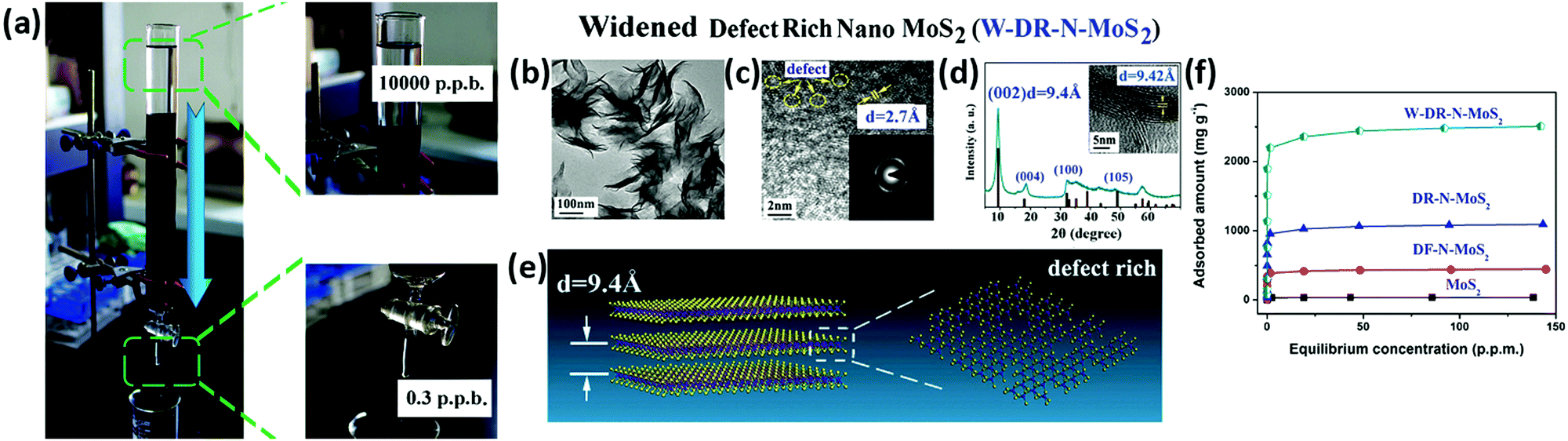 | ||
| Fig. 11 (a) Purification of a natural water sample. The mercury-contaminated water was passed through a purification column filled with W-DR-N-MoS2: (b) TEM image of W-DR-N-MoS2. (c) HRTEM image of the basal plane of W-DR-N-MoS2; the inset shows the corresponding SAED pattern. (d) XRD pattern and the cross-sectional HRTEM image of W-DR-N-MoS2. (e) Structural model of W-DR-N-MoS2 with an enlarged interlayer spacing and multiple defects on the basal planes (the sulphur atoms are yellow and the Mo atoms are purple). (f) Mercury adsorption isotherm, compared with commercial MoS2 powder, DF-N-MoS2 and DR-N-MoS2. Adapted from ref. 395 with permission of Wiley-VCH. | ||
Liu et al. showed that MoS2 exhibits a superior ability to adsorb lead ions.399 MoS2 nanosheets were prepared with an ultrasound assisted electrochemical exfoliation method. As in the case of Hg(II) ions the adsorption capacity of MoS2 towards Pb(II) can be attributed to the coordination of Pb(II) with the S atoms of MoS2. Moreover, the strength of such non-covalent interactions is reinforced by electrostatic adsorption. The experimental Pb(II) uptake capacity of MoS2 was estimated to be as high as 1479 mg g−1. The adsorption followed the Freundlich isotherm model and fitted well with both the pseudo-first-order and pseudo-second-order kinetic models. The adsorption of Pb(II) on MoS2 materials was further confirmed by SEM-EDS (Fig. 12a–d) and XPS measurements (Fig. 12e). The immobilization of heavy metal ions on 2DMs is depicted in Fig. 12f. The adsorption might be attributed to the chemical adsorption due to the complexation of Pb(II) with intrinsic S or O atoms exposed on the MoS2 surfaces, together with electrostatic adsorption.
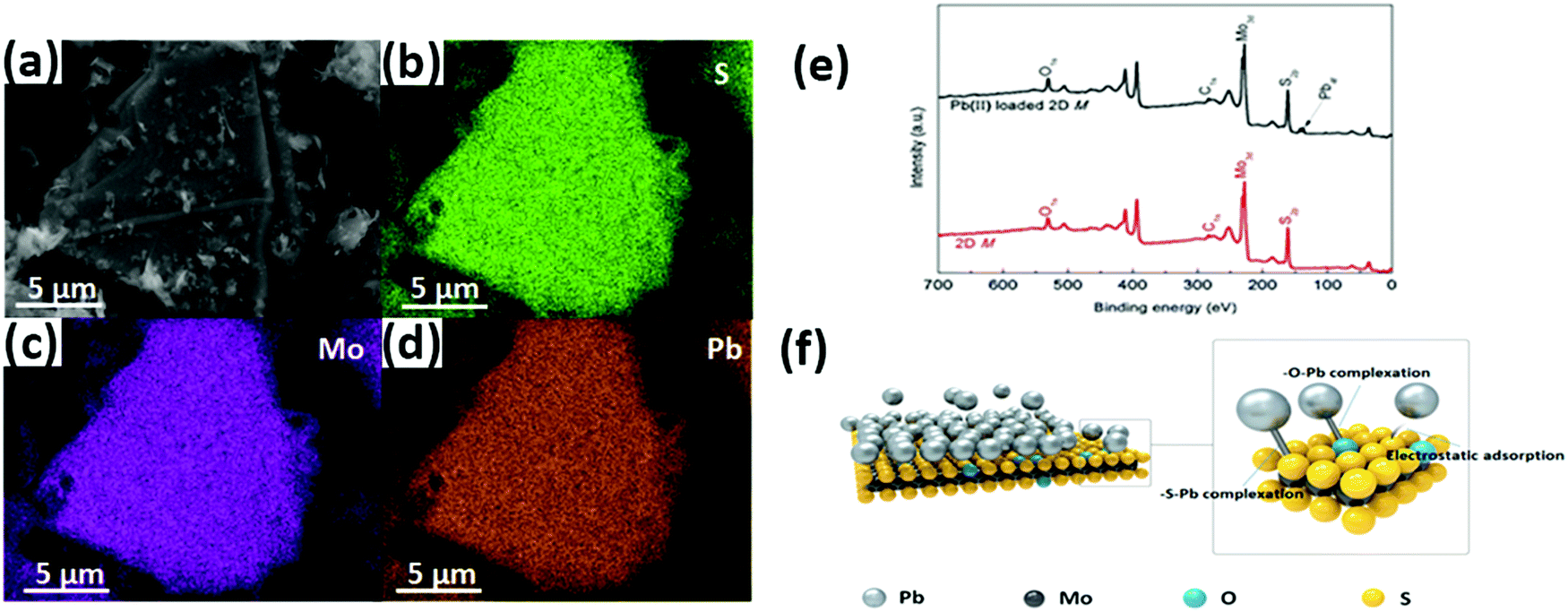 | ||
| Fig. 12 (a) SEM image of a Pb(II) loaded 2DM. (b–d) SEM-EDS elemental mapping images of S, Mo, and Pb, respectively. (e) XPS survey spectra of 2DM before and after Pb(II) adsorption. (f) Diagrammatic illustration of the mechanism for Pb(II) adsorption on the 2DM. Adapted from ref. 399 with permission of Elsevier Ltd. | ||
Other studies showed that the modification or the use of MoS2 as a component of a hybrid material does not increase the qmax towards Pb(II)399,400 and Hg(II)395,401,402 (see Table 7).
| Adsorbent | Contaminant | q max (mg g−1) | Conditions | Ref. |
|---|---|---|---|---|
| List of abbreviations. W-DR-N-MoS2: widened defect rich nano molybdenum disulfide, Au: gold.a Qmax values were calculated using Langmuir isotherms.b Qmax values were calculated using Freundlich isotherms. | ||||
| W-DR-N-MoS2 | Hg(II) | 2563a | pH = NA, T = NA | 395 |
| Au/Fe3O4/MoS2 | 1527a | pH = 5, T = 293 K | 402 | |
| MoS2 | 305b | pH = 6, T = 308 K | 401 | |
| MoS2 | Pb(II) | 1479b | pH = 5, T = 308 K | 399 |
| Co–MoS2 | 660a | pH = 1–6, T = 293 K | 400 | |
| Mn–MoS2 | 588a | pH = 1–6, T = 293 K | 400 | |
3.2 Fluorescence-based metal sensors
Colorimetric sensors for metal ions comprise two key features, i.e. a metal chelating or binding (coordination) pocket and at least one fluorophore capable of absorbing and/or emitting light. Fluorescence sensing is based on analyte-induced changes in the physicochemical properties of fluorophores, including fluorescence intensity, lifetimes, and anisotropy, which are related to charge transfer or energy transfer processes.403 To function as a sensor, the electronic structure of the sensor must be altered upon metal binding. Changes in the electronic structure of the sensor can lead to the changes in the intensity or wavelength of light absorption or emission, while changes in the molecular structure can modify the distance or alignment between a pair of fluorophores that serve as a donor–acceptor pair.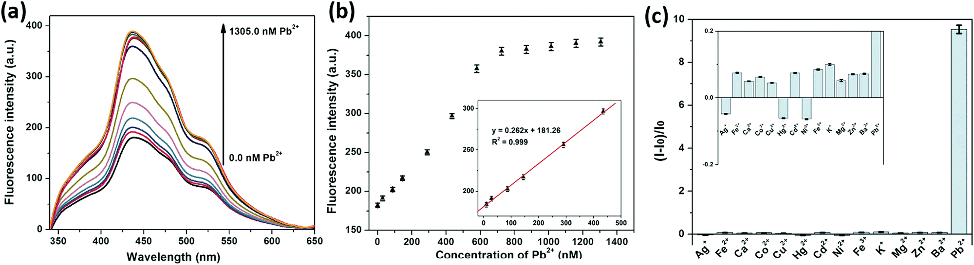 | ||
| Fig. 13 (a) Fluorescence recovery of the aptamer–rGQD/GO system after incubation with various concentrations of Pb2+ (0.0, 29.0, 87.0, 145.0, 290.0, 435.0, 580.0, 725.0, 870.0, 1015.0, 1160.0, 1305.0 nM). (b) Linear relationship between the fluorescence intensity and the concentration of Pb2+. (c) Fluorescence intensity changes (I − I0/I0) of the sensor in the presence of various metal ions. Adapted from ref. 306 with permission of Elsevier Ltd. | ||
Li et al. demonstrated that the single-stranded DNA (ssDNA) aptamer attached on GO can specifically bind to the mercury ions, leading to the formation of a hairpin-shaped double-stranded DNA (dsDNA) structure.307 The water-dispersible GO sheets, which are functionalized with the ssDNA aptamer, exhibit strong fluorescence emission at 600 nm under excitation at 488 nm in the absence of Hg(II) ions. When Hg2+ ions appear in the aqueous solution, they are sandwiched between the hairpin-shaped dsDNA due to the formation of the thymine–Hg(II)–thymine complex, which grasps the Hg2+ ions in proximity to the surface of GO. As a result, the fluorescence emission of GO is quenched. Such a sensor shows a limit of detection as low as 0.92 nM and excellent selectivity towards Hg(II) over a wide range of metal ions including K+, Ag+, Ca2+, Cd2+, Cu2+, Pb2+, Ni2+, Co2+ and Fe3+. Recently, Wen et al. reported a FRET sensor based on a cytosine rich DNA probe and GO.308 In the presence of Ag+, a DNA–Ag+ complex was formed, and the conformation of the probe changed to straight stiff, resulting in the desorption of DNA from the surface of GO and fluorescence recovery (Fig. 14a). Fluorescence spectra of the cytosine-rich oligonucleotide (SSO) probe upon incubation with a series of concentrations of Ag+ and then mixed with GO are portrayed in Fig. 14b. This assay is based on the interaction between the target-induced conformational change of the SSO fluorogenic probe and graphene oxide quenching effects. The use of a simple mix-and-detect analysis revealed a high selectivity toward Ag+ as determined in the presence of ten times higher concentrations of 12 different interference metal ions (Fig. 14c).
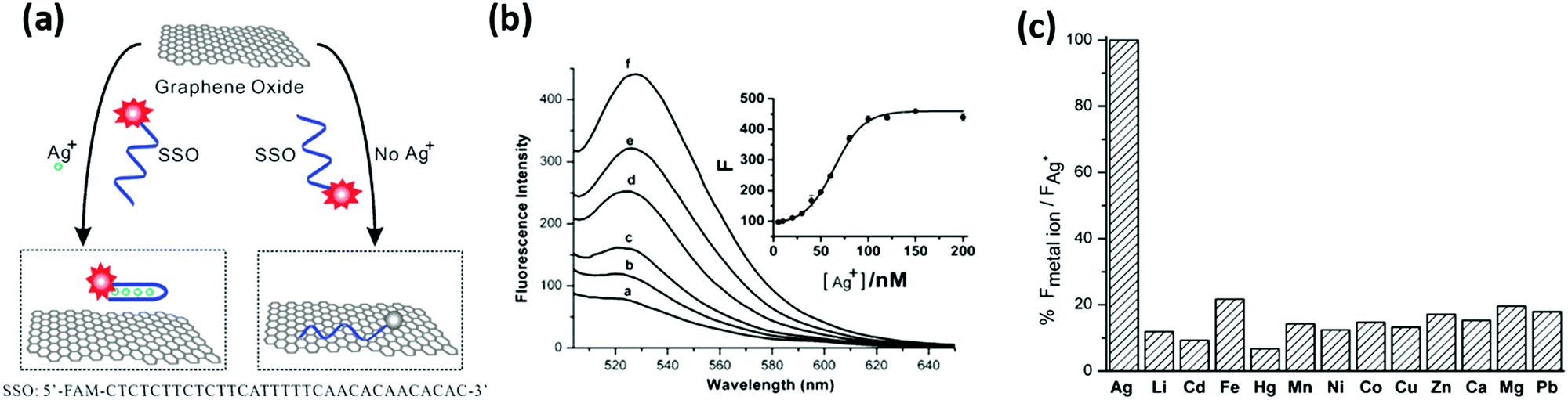 | ||
| Fig. 14 Schematic illustration of the fluorescence sensor for Ag(I) ions based on the target-induced conformational change of a silver specific cytosine-rich oligonucleotide (SSO) and the interactions between the fluorogenic SSO probe and graphene oxide: (a) FAM-labelled silver-specific oligonucleotide probe. (b) Fluorescence spectra of the SSO probe upon incubation with a series of concentrations of Ag+ and then mixed with GO: a 0 M, b 20 nM, c 40 nM, d 60 nM, e 80 nM and f 150 nM. All experiments were carried out in MOPS buffer (10 mM, pH 7.0) containing 50 mM NaNO3 and 10 nM SSO. Ag+ of different concentrations were incubated in this solution for 5 min at 23 °C and then the fluorescence spectra were recorded 2 min after GO (10 mg) was added to this mixture. λex = 494 nm. (c) Selectivity of the analysis of Ag+ ions in the presence of different metal ions. The concentration of Ag+ was 100 nM, whereas all other interference metal ions were 1 μM. Adapted from ref. 308 with permission of the Royal Society of Chemistry. | ||
Recently, a fluorescent nanoprobe based on MoS2 nanosheets for selective and ultrasensitive detection of Ag+ (down to 10 nM) ions alike in aqueous solutions and biological cells (Escherichia coli) was developed by Yang et al.310 In this study AgI ions were reduced to Ag0, which led to the detachment of rhodamine B isothiocyanate (RhoBS) non-covalently interacting with MoS2 nanosheets, which resulted in the quenching of its fluorescence (see Table 8 for details).
| Material | Analyte | Linear range | Detection limit | Ref. |
|---|---|---|---|---|
| List of abbreviations. TPPS: tetraphenylporphyrin tetrasulfonic acid. | ||||
| MoS2 | Ag(I) | 10–500 nM | 1 nM | 309 |
| WS2 | 5.0–1000 nM | 1.2 nM | 313 | |
| Hg(II) | 6.0–650 nM | 3.3 nM | 313 | |
| B,N-MoS2 | 0.01–3 μM | 1 nM | 311 | |
| BP-TPPS | 1–60 nM | 0.39 nM | 317 | |
| MoS2 | Pb(II) | 0.5–12 μM | 0.22 μM | 312 |
| BP-fibres | 0.1–1.5 × 10⁷ ppb | 0.25 ppb | 315 | |
An interesting approach for enhancing the fluorescence of MoS2 was proposed by Liu et al.311 and it relies on covalent modification of MoS2 nanosheets with either boron or nitrogen atoms. Boron and nitrogen doping results in changes in the band gap of MoS2, which increases from 1.20 eV to 1.61 eV. The as-prepared B- and N-doped MoS2 nanosheets were used as facile, green, label-free and effective sensing platforms for Hg2+ ions. The modified nanosheets exhibit enhanced fluorescence properties compared with the undoped MoS2, which were highly quenched after selective absorption of Hg2+. Wang et al. found that after the doping with Pb2+ ions the fluorescence of MoS2 nanosheets was enhanced, which was subsequently quenched by the addition of sulphide ions.312 The fluorescence quantum yield measurements of the single layer MoS2 was estimated to be ∼0.28%. The quantum yield of the doped MoS2 nanosheets was calculated to be ∼0.73%, thereby indicating that molecular doping of MoS2 nanosheets with lead(II) metal ions strengthened their fluorescence.
To date, little has been done on the application of WS2 nanosheets in biological and chemical sensing. For example, Zuo et al. developed a novel dual-colour fluorescence biosensing platform based on WS2 nanosheets.313 The sensor could achieve simultaneous detection of Hg2+ and Ag+ in a high sensitivity and wide linear range by monitoring fluorescence intensity changes at 525 nm and 583 nm, respectively. Hg2+ and Ag+ were selectively detected in the concentration range from 6.0 to 650.0 nM and from 5.0 to 1000.0 nM, with detection limits of 3.3 nM and 1.2 nM, respectively. The fluorescence intensities in the presence of other heavy metal ions changed by ∼5% when the cation concentrations were 10-fold greater than those of Hg2+ and Ag+ ions, indicating that the developed biosensor is highly selective for mercury and lead ions.
Gu et al. presented a novel ratiometric fluorescence sensor based on the inner filter effect (IFE) of tetraphenylporphyrin tetrasulfonic acid (TPPS) toward black phosphorus quantum dots (BP QDs), developed for the selective and sensitive detection of Hg2+.317 Highly fluorescent BP QDs were successfully synthesized from bulk BP by a sonication-assisted solvothermal method. In the presence of Hg2+, the IFE originating from the spectral overlap between the excitation of BP QDs and the absorption of TPPS is inhibited, resulting in the recovery of the fluorescence of BP QDs. The constructed sensor revealed a good linear response to Hg2+ ranging from 1 to 60 nM with a detection limit of 0.39 nM. Interestingly, this strategy could also be applied in the determination of Hg2+ in real water samples with satisfactory results. Sensing properties for all 2DM-based fluorescent sensors are presented in Table 8.
3.3 Field-effect transistor based metal sensors
2DM nanosheets integrated into FETs have recently revealed their enormous potential for detection of heavy metals. The working principle of a 2DM-based FET sensor is based on the changes in the critical parameters of a FET containing 2DM nanosheets upon adsorption of targeted heavy metal ions. This includes primarily the field-effect mobility, threshold voltage and Ion/Ioff ratio. 2D semiconducting sheets are of particular interest because of their high charge carrier mobility and very high surface-to-volume ratio, leading to high sensitivity. Chemical sensors based on FETs can overcome the obstacles of previous detection methods. For example, the aforementioned optical methods have some limitations such as multiple sensing steps, the need for using chemical agents, a higher cost, and a longer detection time. In contrast, the use of 2DM-based FET sensors enables the rapid label-free detection of metal ions in real-time by monitoring the resistance or the Dirac point shift caused by the adsorption of target analytes. Such devices can be characterized also by low power consumption and can be miniaturized for the development of portable sensors, eventually supported on flexible foils.Alternative approaches based on solution processable rGO,291,292 and G functionalization92,293–295 are being pursued with the ultimate goal of developing low-cost, scalable fabrication of graphene-FET sensors. Recently, Sudibya et al. presented a FET sensor using micropatterned, metallothionein type II protein (MT II)-functionalized rGO films, which bind with both physiological (e.g., Cu2+, Zn2+) and xenobiotic (e.g., Hg2+, Cd2+) metal ions with high affinity (see the schematic illustration in Fig. 15a).291 A typical plot of drain-to-source current (Ids) versus solution-gate voltage (Vg) of a rGO-FET sensor is displayed in Fig. 15b. Such a nanoelectronic sensor is capable of detecting various metal ions in real-time with high sensitivity. The addition of mercury (Hg2+), at a concentration as low as 1 nM, caused an obvious current increase in the rGO-FET which was biased at Vds = 400 mV and Vg = −0.6 V (Fig. 15c). The magnitude of the device response scales with the Hg2+ concentration, and its polarity depends on the gate voltage (Vg). The detection limit for Hg2+ was estimated to be as low as ∼1 nM with a signal-to-noise ratio of 25–30 (Fig. 15d). The very same device exhibited also Cd2+ detection at 1 nM with a slightly smaller change in the current signal-to-noise ratio of 15–20 (Fig. 15e).
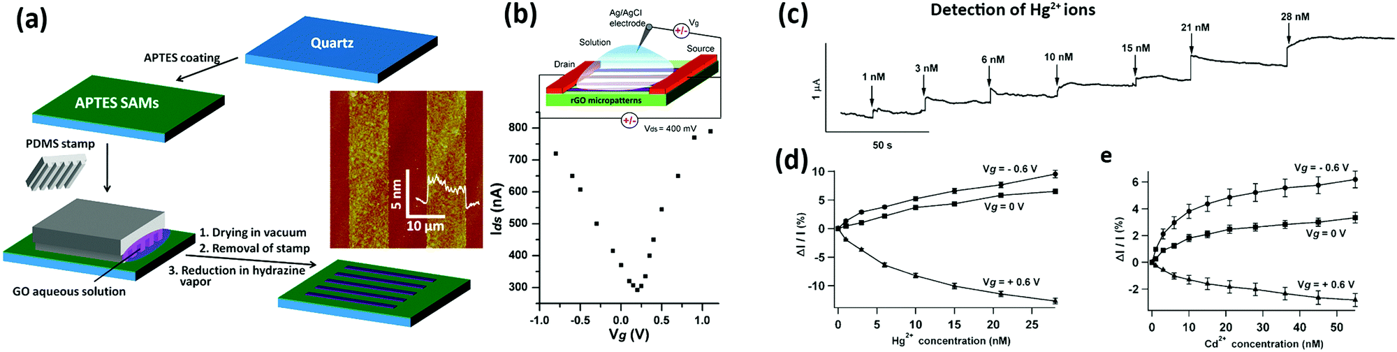 | ||
| Fig. 15 (a) Schematic illustration for the fabrication of patterned rGO thin films on APTES-coated quartz. Inset: AFM image of the obtained rGO micropatterns on APTES-coated quartz. (b) Ambipolar characteristics of the rGO-FET measured in 0.1 M phosphate buffer saline (PBS) solution. Inset: Schematic of a solution-gated configuration of rGO-FET. (c) Typical real-time recording of Ids with the addition of Hg2+ ions. (d and e) Change in Ids in rGO-FETs (number of tested samples, n = 6) with the addition of (d) Hg2+ and (e) Cd2+ ions at Vds = 0.4 V and Vg = −0.6 (circles), 0 (squares), and +0.6 V (triangles). Adapted from ref. 291 with permission of American Chemical Society. | ||
For heavy metal ion GFET sensors, biomolecules are frequently used as sensing nanoprobes due to their high binding affinity to inorganic contaminants.92 An et al. reported a high-performance flexible graphene aptasensor for Hg2+ detection.293 1,5-Diaminonaphthalene (DAN) and glutaraldehyde (GA) were employed as cross-linking agents, while the aptamer (3′-amine-TTC TTT CTT CCC CTT GTT TGT-C10-carboxylic acid-5′) was non-covalently linked onto the graphene surface as a probe for Hg2+. The field-induced responses from the graphene aptasensor showed excellent sensing performance: Hg2+ ions with a very low concentration of 10 pM could be detected (Fig. 16a), which is 2–3 orders of magnitude higher than previously reported mercury sensors using electrochemical devices.406,407 A GFET-sensor was characterized with the experimental setup presented schematically in Fig. 16b. The sensor response time was rapid, with values below 1 s. Noteworthily, the pristine graphene devices showed no significant current changes upon exposure to Hg2+. It was concluded that the origin of current changes in the sensor relies on the p-doping effect resulting from the thymine–Hg–thymine complex formed between Hg2+ ions and thymine base pairs in the aptamer (Fig. 16c).
 | ||
| Fig. 16 (a) Real-time response curve of the aptasensor with various Hg2+ concentrations (10 pM to 100 nM). Graphene substrate without the aptamer was introduced as a control sample. (b) Schematic diagram of a liquid-ion gated FET using graphene conjugated with the aptamer (Vg, S and D indicate the gating voltage and source/drain electrodes). (c) Interaction of Hg2+ ions with thymine base pairs in the aptamer immobilized on the surface of the modified graphene layer. (d) Selective responses of the aptasensor toward the target metal ions (Hg2+, 10 pM) and nontarget metal ions (Cd2+, Co2+, Ni2+, Na+, Pb2+, Sr2+ and Zn2+, 10 mM). Adapted from ref. 293 with permission of American Chemical Society. | ||
Noteworthily, graphene-based FET sensors can be exploited for the detection of not only heavy metal ions (e.g. Hg2+ and Pb2+) but also alkali metal ions in water including K+294 and Na+.295
Jiang et al. demonstrated a FET based on mechanically exfoliated few-layer MoS2 nanosheets for sensing Hg2+ ions.296 The interaction between Hg2+ ions and few-layer MoS2 was studied using FET measurements and photoluminescence. Due to the high binding affinity between the sulphur sites on the MoS2 surface and Hg2+ ions, the latter can strongly bind to MoS2. Remarkably, it was shown that the binding of Hg2+ results in a p-type doping and reduces the electron concentration in n-type few-layer MoS2. Upon binding Hg2+ ions the electron transport and photoluminescence properties in few-layer MoS2 are effectively modulated. It was also demonstrated that by monitoring the changes in the conductance of few-layer MoS2 and varying the concentration of Hg2+ solutions, few-layer MoS2 transistors can function as highly sensitive sensors for rapid electrical detection of Hg2+ with a detection limit as low as 30 pM.
Zhou et al. reported on a DNA-functionalized MoS2 nanosheet/gold nanoparticle hybrid FET sensor for the ultrasensitive detection of Hg2+ in an aqueous environment (Fig. 17a).297 A thin film was formed by filtration of MoS2 nanosheets produced by liquid-phase exfoliation, followed by transfer onto the Au electrodes and thermal annealing. Then Au NPs were sputtered onto the MoS2 film, and finally the DNA molecules were grafted onto Au NPs by immersing the device in a DNA solution. In the hybrid structure, the MoS2 thin film acts as the conducting channel with the homogeneously dispersed Au NPs operating as anchoring sites for DNA probes chosen to specifically target Hg2+ ions. Upon addition of Hg2+ to the sensor, the formation of metal complexes between the thymidine bases present in the DNA molecules and mercury ions takes place, resulting in the changes in the MoS2 conductance. The detection of metal ions was enabled by monitoring the change in the source–drain current in the FET device as a function of Hg2+ concentration. The detection limit of the sensor can reach values down to the concentration of 0.1 nM (Fig. 17b). It was shown that the rate of the increase in the conductance or source–drain current is dependent on the Hg2+ concentration (Fig. 17c). The sensor was also tested with a series addition of Hg2+ and the dynamic responses indicated that the sensor responded to Hg2+ within a few seconds, which is much faster than the conventional optical methods. The output characteristics of three types of sensors, i.e. MoS2, MoS2–Au NPs, MoS2/DNA–Au NPs, are shown in Fig. 17d. Because of the work function difference between the Au NPs (3.6 eV in air for D = 8 nm) and the MoS2 film (∼5.23 eV after annealing), electron transfer occurs from the Au NPs to the MoS2 film, leading to a decreased concentration of holes in the MoS2 film and thus the decreased conductivity.
 | ||
| Fig. 17 (a) FET sensor platform based on the hybrid structure. The formation of T–(Hg2+)–T chelates, through reaction between Hg2+ and the thymidine bases exposed on the DNA molecules grafted onto the Au NPs, leading to the change in the MoS2 electrical conductivity as a sensor signal. (b) Real-time detection of Hg2+ (nM) in water (Vds = 0.1 V) with platforms of MoS2/DNA–Au NPs (black, solid), MoS2–Au NPs (purple, dashed), and MoS2 (blue, short dashed), respectively. (c) Sensitivity variation and exponential fitting of sensitivity as a function of Hg2+ concentration for the MoS2/DNA–Au NP hybrid sensor. (d) Evolution of the Ids–Vds characteristics during the MoS2/DNA–Au NP hybrid sensor fabrication process (Vds = −2.1 V to 2.1 V, step = 0.1 V) at room temperature. Adapted from ref. 297 with permission of American Chemical Society. | ||
Despite the examples discussed in this Review, little knowledge has been gathered on the sorption capacities of other metal ions on 2D MoS2. Therefore, it is of significant importance to extend in the future the application of such 2DM for the detection or removal of other heavy metals considering its markedly high metal capture capacity.
The same group also demonstrated air stable high-performance BP chemical sensors encapsulated with ionophores (Fig. 18a, inset).316 Without protection, BP samples once exposed to air start to degrade and oxygenated phosphorus (POX) is shortly formed, with degradation of its electrical properties and device performances. The ionophore film effectively reduces negative factors from the ambient environment; meanwhile, it displays selective permeability towards certain types of molecules. The ionophore-encapsulated BP devices were found to be still in good shape after 1 week of ambient exposure, with source–drain current Ids variation less than 10% (Fig. 18a). The methodology of the preparation of thin BP nanosheets is the same as the one shown above (i.e. mechanical exfoliation with Scotch tape). The BP sensors were sensitive to the detection of multiplex ions such as AsO2−, Hg2+, Cd2+, and Pb2+ with detection limits down to 10, 1, 3 and 1 ppb, respectively. Moreover, Pb2+ ions can be effectively detected over a wide concentration range, from 10 ppb to 100000 ppb (Fig. 18b). The detection limit and response rate of BP are both better than those reported for graphene based sensors.
 | ||
| Fig. 18 (a) Schematic view of a BP sensor with Idsvs. Vgs curves of BP with ionophore protection. Ids variation is less than 10%, suggesting significantly improved air stability. (b) ΔR/R0versus Pb2+ concentration (experimental results from 7 sensors) and a schematic view of BP sensors with lead ionophores. The resistance of BP becomes saturated at higher concentrations. Experimental results demonstrate a good linear relation between C/ΔG and C, fitting well the Langmuir adsorption isotherm, as shown in the inset. Adapted from ref. 316 with permission of American Chemical Society. | ||
Although only a few biosensors and water sensors with BP FETs were reported due to the inherent instability of BP in a moisture rich environment, BP sensors have attracted increasing interest across the sensing community due to the 2D structure, tuneable band gap, and high carrier mobility of BP. From a practical application standpoint, the thickness, uniform control, and stability of BP limit its application in ultrasensitive sensor technology. With further understanding of interactions between BP and oxygen/water and the improvement of sensor fabrication techniques, BP-based FET sensors can be foreseen to provide a robust sensing method for a wide variety of target analytes in the near future.
3.4 Electrochemical based metal sensors
Electrochemical sensing of heavy metal ions relies on the use of sensing electrodes that are employed for passing the current to an aqueous solution and generate an electrical signal that corresponds to the electrochemical reaction within the solution due to the presence of metal ions. Common experimental setups for electrochemical detection of heavy metal ions consist of an electrolytic cell containing an electrolyte, i.e. a solution of heavy metal ions, in contact with an electrode. The cell potential is measured at the interface of the electrode with the electrolyte solution. Noteworthily, because heavy metal ions have defined redox potentials, the selectivity toward specific heavy metal ions can be achieved using bare electrodes without the need for a molecular recognition probe. Numerous techniques have been employed in electrochemical sensing, including potentiometry, voltammetry, impedimetry, amperometry and conductometry. In particular, the anodic stripping voltammetry (ASV) method is widely explored for detection of heavy metals. ASV analysis typically involves two steps, i.e. deposition of heavy metals onto the electrode surface, and stripping or dissolution of the deposited analyte from the electrode surface. Recent advances in the field have revealed the potential of 2DMs in electroanalysis. Several electrochemical sensors based on 2DMs for bioanalysis and environmental analyses have been developed. In particular, Zhao et al. presented for the first time that Hg2+ can be selectively identified using a PPy–rGO nanocomposite-modified glassy carbon electrode (GCE).299 Such selectivity was achieved using square wave anodic stripping voltammetry (SWASV), which determines a reduction of adsorbed Hg2+ to Hg0 at a certain potential. The anodic stripping current was obtained in a potential range for the identification of Hg2+. In addition, excellent sensitivity (0.124 μA nM−1) and limit of detection (LOD) (15 nM) results were achieved. The measured stripping current toward Hg2+ at the PPy modified electrode was found to be 3–9 times higher than those towards other ions, indicating that rGO in the nanocomposite plays an important role in highly selective detection.Sahhoo et al. reported a facile in situ approach for the fabrication of a rGO/bismuth (Bi) nanocomposite by employing modified Hummers’ method without the use of any surfactants. Bi nanoparticles were uniformly anchored onto the surfaces of individual graphene nanosheets, which prevent restacking of rGO, resulting in good dispersion in solvents. The rGO/Bi nanocomposite was used as an electrode material for the stripping voltammetric determination of heavy metal ions in water. The detection limits of the proposed electrochemical sensor for Cd2+, Pb2+, Zn2+ and Cu2+ were found to be 2.8, 0.55, 17 and 26 ppb, respectively.300 Wei et al. developed a SnO2/rGO-based electrochemical sensor, which could simultaneously and selectively analyse four heavy metal ions such as Cd(II), Pb(II), Cu(II) and Hg(II).301 SWASV has been employed for the detection of heavy metal ions (Fig. 19a). The SnO2/rGO nanocomposite modified glass carbon electrode synthesized by a simple wet chemical method showed enhanced sensing performance compared with single SnO2 and single rGO (Fig. 19b).
 | ||
| Fig. 19 (a) Square wave anodic stripping voltammetry (SWASV) curves for 0.5 μM each of Cd(II), Pb(II), Cu(II), and Hg(II) on bare (violet line), graphene oxide (black line), reduced graphene oxide (red line), SnO2 nanoparticle (blue line), and SnO2/reduced graphene oxide nanocomposite (pink line) modified GCEs in 0.1 M acetate buffer (pH 5.0). Deposition potential = −1.0 V; deposition time = 120 s; amplitude = 25 mV; incremental potential = 4 mV; frequency = 15 Hz; vs. Ag/AgCl. (b) Cyclic voltammograms measured with bare, GO, rGO, SnO2 nanoparticle, and SnO2/reduced graphene oxide nanocomposite modified GCEs in a solution of 5 mM Fe(CN)63−/4− containing 0.1 M KCl. Inset: Nyquist diagram of electrochemical impedance spectra for bare and SnO2/reduced graphene oxide nanocomposite modified GCEs in the solution of 5 mM Fe(CN)63−/4− containing 0.1 M KCl. Adapted from ref. 301 with permission of American Chemical Society. | ||
Li et.al. used Nafion and rGO for anodic stripping voltammetric analysis of cadmium with a detection limit 0.005 ppb.302 Willemse et al. reported on the determination of Cd2+, Pb2+, Zn2+ and Cu2+ by making use of a platform based on a Nafion–graphene nanocomposite film.409 LODs of 0.07–0.08 ppb have been achieved for the individual ions, which are comparable to those determined with ICP-MS, and ascribed to a combination of the enhanced electron conduction of rGO and the cation exchange capacity of Nafion. Similarly, Chaiyo et al. constructed a Nafion/ionic liquid/graphene electrochemical sensor for simultaneous determination of zinc, cadmium and lead using screen-printed carbon (Fig. 20a).303 The functionalized graphene-based nanocomposite modified electrode showed better detection performance for Zn(II), Cd(II) and Pb(II) compared to the bare electrode by SWASV (Fig. 20b). The detection limits of such sensors for Zn(II), Cd(II) and Pb(II) detection were 0.09 ng mL−1, 0.06 ng L−1 and 0.08 ng L−1, respectively.
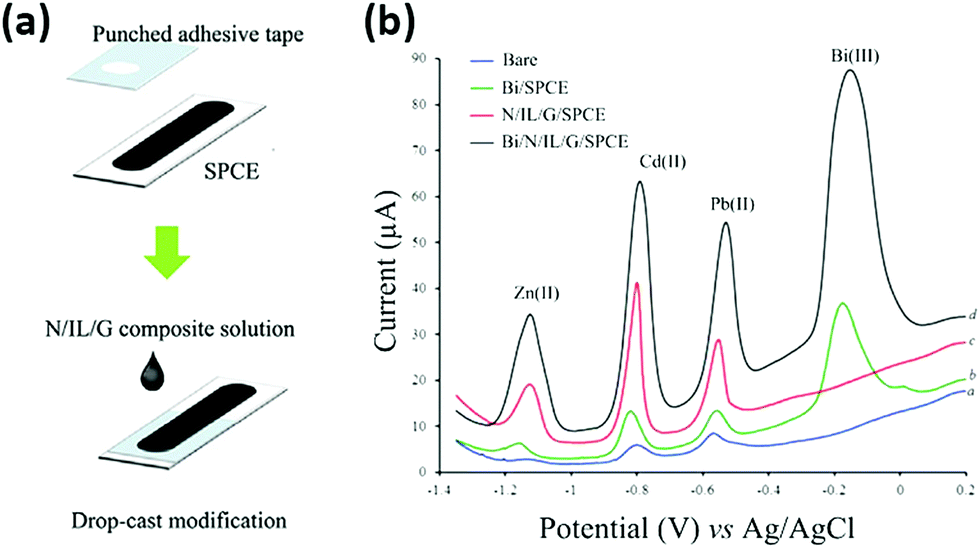 | ||
| Fig. 20 (a) Schematic drawing of the electrochemical sensor fabrication. (b) Square wave anodic stripping voltammetry (SWASV) curves of 50 ng mL−1 Zn(II), Cd(II) and Pb(II) in 0.1 M acetate buffer solution (pH 4.5). Adapted from ref. 303 with permission of Elsevier B.V. | ||
Gong et al. reported an ultrasensitive Hg(II) electrochemical sensor using monodispersed Au nanoparticles onto the graphene nanosheet matrix as the enhanced sensing platform.410 The detection limit was found to be as low as 6 ppt. The interference from other heavy metal ions such as Cu2+, Cr3+, Co2+, Fe3+, Zn2+and I− ions associated with Hg2+ analysis could be effectively inhibited. Another example relies on the use of cysteine-functionalized GO (sGO) and carbonyldiimidazole as a cross-linker via the formation of amide and carbamate bonds. A sGO/polypyrrole (PPy) nanocomposite film was grown on the working electrode surface of a screen-printed electrode (SPE) via controlled one-step electrochemical deposition.304 The sGO/PPy-SPE was used to detect lead ions in water by differential pulse voltammetry (DPV). The DPV signals were linear in the range of 1.4–14000 ppb of Pb2+. The measurable detection limit of the sensor is 0.07 ppb, which is 2 orders of magnitude below the threshold value for drinking water set by the World Health Organization. The average removal efficiency of Pb2+ deposited on the electrode amounted to 99.2%, with a relative standard deviation (RSD) of 3.8%. The selective detection of the GO/PPy composites was investigated by mixing GO/PPy with various metal ions such as Pb2+, Na+, Mg2+, Cd2+, Cu2+, Hg2+ and Ag+. The results clearly show that the GO/PPy composite film can selectively detect Pb2+ and remains unresponsive in the presence of other metal ions. In addition, the developed device can be used multiple times.
TMD nanostructures were mainly utilized as sensing platforms for the development of electronic and fluorescent sensors, while their electrochemically sensing applications are still limited. Cui et al. synthesized a monolayer MoS2 supported Cu7S4–Au nanocomposite as a sensing platform to detect Hg(II) using an anodic stripping voltammetric technique.305 They found that the synergistic effects of both Au domains and active edge sites of monolayer MoS2 played a vital role in the high-performance detection of Hg(II) with a limit of detection of 190 nM.
In this part of the Review article, we have provided an overview on the recent advances in metal ion sensing. Different types of 2DMs employed for specific and selective recognition of heavy metals have been discussed in this section. By taking advantage of their unique properties, 2DMs can be successfully explored to construct a wide range of optical and electrical sensing platforms for the detection of various heavy metal ions. Chemical modification of GO and TMDs has proven to provide a promising solution for improving the sensing performance with high specificity, enhanced sensitivity and a low detection limit. Chemical metal sensors based on 2DMs have demonstrated high sensitivity detection of a wide variety of heavy metal ions at low concentrations, due to the maximum sensor surface area per unit volume. Their favourable structural and compositional synergy allows them to be excellent electrode materials for fabricating various fluorescent and electrochemical sensing platforms, such as FET-based sensors. Moreover, electrochemical measurements have shown numerous advantages for trace heavy-metal detection, including rapid analysis, good selectivity, and sensitivity. Optical detection systems are other alternatives to the electrochemical detection methods. They represent attractive analytical tools whenever continuous monitoring and real-time information are desired.
4 (Bio)molecular sensors
4.1 (Bio)molecular sensing with graphene, graphene oxide and related composites
Ultrafast sensing of chemically and biologically active molecules at low concentrations is critical in a wide range of research fields and in particular for applications, such as chemical analysis,411 healthcare,412,413 and monitoring the environment or diagnostic diseases.414 Because of their particular physico-chemical properties, graphene-based materials have been used to fabricate various types of chemical sensors including electrochemical,72,413,415–444 FET,445–449 fluorescent450–457 and surface enhanced Raman spectroscopy-based sensors.411,458–460 Graphene based materials have been used to develop various types of sensors to detect molecules such as glucose,72,415–423,425,427,445,461–465 DNA,72,428,430,447,449,451,452,455,457,466–469 hydrazine,431,470–473 dopamine,72,413,424,432–439,441,454,474,475 ascorbic acid,72,413,434,441,476,477 H2O2,72,443,478–480 and other aromatic molecules (Fig. 21).411,453,456,458,459,478 Graphene-based materials offer various advantages, when compared to other carbon-based nanomaterials like CNTs or fullerenes. In particular, graphene can be easily produced from bulk graphite via exfoliation.126,481–483 Moreover, the particular strength of graphene, the quality of its crystal structure, and its band structure and high conductivity allow the preparation of devices with extremely low noise levels and relatively low 1/f noise.448 | ||
| Fig. 21 Differential pulse voltammograms (DPVs) recorded using (a) a GC electrode, (b) a graphite/GC electrode, and (c) a CR-GO/GC electrode, for guanine (blue), adenine (orange), thymine (violet), and cytosine (magenta), respectively. Adapted from ref. 72 with permission of American Chemical Society. | ||
As mentioned above, the majority of graphene-based sensors rely on the chemical modification of GO, which exhibits numerous oxygen-rich functional groups that can interact via dipole–dipole or strong electrostatic interactions with (charged) molecules, or it can be covalently functionalized with functional molecules, enhancing the occurrence of adsorption events. In particular, covalent grafting of organic molecules onto GO offers the flexibility for various functionalizations to enhance the sensor performance. Moreover, the combination of its abundant structural defects and chemical groups facilitates the charge transfer and thus ensure high electrochemical activity. Noteworthily, the chemical and electrical properties of rGO are highly tuneable and can be engineered through control of the reduction process.
Zhou et al. exploited a chemically reduced GO modified glassy carbon electrode (CR-GO/GC) for electrochemical sensing of free purine and pyrimidine acids and several other biologically active molecules.72 It was demonstrated that the CR-GO/GC electrode provides greater electrocatalytic activity to guanine (G), adenine (A), thymine (T) and cytosine (C) oxidation than commonly used glassy carbon (GC) and graphite/glassy carbon graphite/GC electrodes (Fig. 21). Moreover, presented electrode exhibited enhanced analytical performance toward detection of glucose, ethanol, dopamine and other biological molecules. In particular, while the amperometric measurement of reduced nicotinamide adenine dinucleotide (NADH) exhibited a faster response time, a wider linear range (40–800 μM), a lower detection limit (10.00 μM) and higher sensitivity (2.68 μA mM−1 cm−1). Gao and co-workers carried out the chemical reduction of GO, obtaining a hydroxyapatite/rGO composite, used as an effective electrochemical sensor of hydrazine.472 The composite dispersed in 1% acetic acid was applied on a GCE and dried, resulting in a high-performance electrode with outstanding performance of the electrocatalytic oxidation of N2H4. The as-prepared electrode exhibited a synergistic effect of the components during detection of hydrazine, which is greater than those of the electrodes fabricated with rGO and hydroxyapatite separately. Wang and co-workers devised a facile approach relying on the efficient preparation of nitrogen-doped graphene via nitrogen plasma treatment of chemically synthesized graphene, which exhibits excellent electrocatalytic activity toward hydrogen peroxide reduction.415 Detection of H2O2 as one of the products of catalytic glucose oxidation can be applied for selective and sensitive glucose determination during enzymatic processes. Noteworthily, a N-doped graphene electrode exhibited high concentration-dependent response and was able to detect up to 0.01 mM glucose in the presence of interferents. N-Doped electrodes can also find their use in detection of important biomolecules such as ascorbic acid (AA), dopamine (DA) and uric acid (UA).413 Efficient oxidation and large peak separation provide simultaneous determination of those three biomolecules with detection limits up to 2.2 × 10⁻⁶, 2.5 × 10⁻⁷ and 4.5 × 10⁻⁸ M for AA, DA and UA, respectively. Furthermore, a differential pulse voltammetry (DPV) experiment revealed that the electrochemical response of target biomolecules increases linearly with increase of molecule concentration.
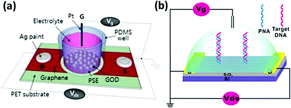 | ||
| Fig. 22 Schematic representation: (a) graphene top gate FET sensor. Adopted from ref. 446 with permission of the American Chemical Society. (b) Graphene oxide back-gate FET sensor. Adapted from ref. 449 with permission of Elsevier. | ||
Huang and co-workers presented a CVD-grown graphene FET sensor functionalized with specific redox mediators for glucose and glutamate detection.445 Glucose sensing is usually based on an enzymatic reaction catalysed by glucose oxidase. Since the products of the oxidation process are H2O2 and gluconic acid, direct measurement of H2O2 is useful for glucose detection. The detection limits were found to be 0.1 mM and 5 μM for glucose and glutamate, respectively. Another CVD-grown glucose sensor was assembled by Kwak et al.446 A solution-gated field-effect transistor (SGFET) was constructed utilizing a graphene channel modulated by the gate potential applied from the top gate electrode and transmitted through the solution. Such a SGFET sensor was exploited to detect glucose in the 3.3–10.9 mM range. Moreover, it provided high resolution and continuous real-time monitoring. To reach the largest sensing response, graphene transistors are operated at the point of maximum transconductance, which leads to large noise that influences the device sensitivity. To avoid such a phenomenon, Fu and co-workers exploited the sensing properties of single layered graphene near its neutrality point.447 This approach led to a significant decrease of the signal-to-noise ratio, thereby making it possible to observe positive signals coming from single stranded DNA (ssDNA) at levels of picomolar concentrations (pM). Moreover, to target specific hybridization corresponding to HIV-virus related ssDNA, functionalization of a GFET surface with pyrene-linked peptide nucleic acid (pPNA) was performed. Noteworthily, the 1/f noise in graphene based FET sensors was found to vary with the number of graphene layers; therefore subsequent optimization of this class of sensors is anticipated.448 Another approach in which hydrazine-reduced GO was used to fabricate a FET sensor on a SiO2/Si substrate was proposed by Cai et al.449 A DNA sensor was prepared by drop-casting a rGO suspension onto a sensing channel as the conducting material. 1-Pyrenebutanoic acid succinimidyl ester (PASE) used as a molecular linker was fixed on the graphene surface via π–π stacking interactions and peptide nucleic acid (PNA) molecules were covalently anchored. Subsequently, a complementary DNA was applied onto the device and specific hybridization caused a shift of the Ids–Vg curves and allowed the measurement. The detection limit was estimated to be as low as 100 fM.
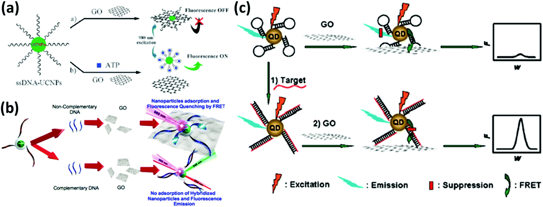 | ||
| Fig. 23 Schematic representations of different FRET mechanisms used in biomolecule sensing. (a) Schematic representation of the upconversion fluorescence resonance energy transfer used for ATP sensing. Adapted from ref. 452 with permission of the Royal Society of Chemistry. (b) FRET mechanism based on quenching ability of GO applied for complementary DNA detection. Adapted from ref. 450 with permission of American Chemical Society. (c) DNA sensing. Molecular beacon decorated QDs quenched by a GO platform, in the presence of complementary DNA, emission is significantly enhanced. Adapted from ref. 451 with permission of American Chemical Society. | ||
Dong and co-workers reported on the FRET from quantum dots (QDs) to GO.451 In particular, the authors demonstrated that QDs substituted with molecular beacon (MB) as a recognition unit towards the targeted molecule can strongly interact with the GO surface, to allow the design of novel sensitive and selective platforms for fluorescence-quenching detection of DNA. In general, GO's quenching properties were used to decrease the fluorescence intensity in the presence of QDs – an effective donor supplied with MB that provides efficient energy transfer to GO (Fig. 23c). Fluorescent graphene quantum dots (GQDs) were also applied for detection of aromatic nitro compounds (e.g. TNT) working as quenchers over a wide range, sustaining the linear correlation.453 Another DNA sensor using FRET between upconversion nanoparticles and GO was reported by Alonso-Cristobal et al.450 The correlation between the concentration of ssDNA (Fig. 24) and luminescence intensity was presented. Its effective detection limit was experimentally shown to be in the picomolar range.
 | ||
| Fig. 24 Up-conversion fluorescence spectra of the UCNPs@SiO2–ssDNA nanoparticles (0.4 mg mL−1) (a) in the presence of different concentrations of GO, and (b) in the presence of different concentrations of complementary ssDNA and 0.3 mg mL−1 of GO. Adapted from ref. 450 with permission of American Chemical Society. | ||
A GO-based platform for DNA and protein sensing reported by Lu and co-workers includes ssDNA supplied with fluorescent organic dye that strongly adsorbs on the GO's surface simultaneously, entailing high quenching efficiency.455 The addition of a complementary ssDNA sequence causes an efficient fluorescence increase and may be used to determine the desired nucleotide sequences. Experiments also proved the dependence on the concentrations of different proteins. The results revealed that the presence of human thrombin might be determined without the interference of the other proteins.
Lu et al. proposed the use of Ag and Au NP-decorated single-layer rGO films anchored on Si surfaces to detect popular organic dyes rhodamine 6G (R6G), methyl violet (MV), rhodamine B (RB) and methylene blue (MB) at nanomolar concentrations.411 Such molecules easily adsorb on the rGO surface, while Ag and Au nanoparticles provide dramatic enhancement in the Raman intensities of the sample. Moreover, a correlation between NP size and observed signals has been monitored, and it could be controlled through the reaction time. Another modification with Ag NPs for ultrasensitive detection of aromatic molecules was demonstrated by Liu and co-workers.458 Additional enhancement of the Raman signals was ensured by GO treated with 3-mercaptopropyltrimethoxysilane (MPTMS), further functionalized with Ag-NPs. An effective detection of differently charged molecules was successfully characterized and presented. In particular, experiments with PPh3 used as the target molecule exhibited limits of detection as low as 10−9 M.
Graphene grown on copper foil and Ag NPs anchored on a Si substrate can also be used to prepare a SERS active substrate for detection of TNT by alkaline hydrolysis.459 High pH values provide efficient hydrolysis of TNT and increase the intensities of Raman spectral signals. Extremely high limits of detection (up to 6.6 × 10⁻¹⁰ M) and an excellent anti-interference ability confirms the perspective potential of SERS sensors. Shanta and Cheng prepared hydrazine reduced GO combined with silver nanoprisms and utilized such a hybrid system for trace detection of tetrachlorobiphenyls (PCBs).460 The as prepared chip successfully allowed multiplex measurements of several environmentally important aromatic compounds. The proposed SERS sensor provided a low limit of detection (up to 100 nM) and simultaneous analysis of multiple isomers.
Values such as the limit of detection and linearity range for detection of various biomolecules are summarized in Table 9.
| Material | Type of sensor | Analyte | Limit of detection | Linearity range | Ref. |
|---|---|---|---|---|---|
| List of abbreviations. DMF: dimethylformamide, AA: ascorbic acid, NPs: nanoparticles, TNT: 2,4,6-trinitrotoluene, NADH: β-nicotinamide adenine dinucleotide, NH2NH2: hydrazine, DA: dopamine, UA: uric acid, QDs: quantum dots, SERS: surface enhanced Raman scattering, R6G: rhodamine 6G, MV: methyl violet, RB: rhodamine B, MB: methylene blue, PPh3: triphenylphosphine, PCB: 2,2′,3,3′-tetrachlorobiphenyl. | |||||
| DMF-exfoliated graphene | Electrochemical | AA | 0.12 mM | 0.4–6.0 mM | 477 |
| Pt-NPs–graphene | H2O2 | 80 nM | 1–500 μM | 478 | |
| TNT | 0.3 ppm | 0.5–40 ppm | |||
| Cu-NPs–graphene | Glucose | 0.5 μM | 0–4.5 mM | 421 | |
| rGO | H2O2 | 0.05 μM | 0.05–1500 μM | 72 | |
| NADH | 10 μM | 40–800 μM | |||
| Hydroxyapatite-rGO | NH2NH2 | 0.43 μM | 2.5 μM–1.16 mM | 472 | |
| N-Doped graphene | Glucose | 0.01 mM | 0.1–1.1 mM | 415 | |
| N-Doped graphene | AA | 2.2 μM | 5.0–1300 μM | 413 | |
| DA | 0.25 μM | 0.5–170 μM | |||
| UA | 4.5 × 10⁻⁸ M | 0.1–20 μM | |||
| CVD-grown graphene | FET | Glucose | 0.1 mM | — | 445 |
| Glutamate | 5 μM | 5–1200 μM | |||
| CVD-grown graphene | Glucose | — | 3.3–10.9 mM | 446 | |
| CVD-grown graphene | DNA | 2 pm | — | 447 | |
| rGO | DNA | 100 fM | 10 fM–1 nM | 449 | |
| QDs–GO | Fluorescent | DNA | 12 nM | 50–1500 nM | 451 |
| Graphene QDs | TNT | 2.2 μM | 4.95 × 10⁻⁴–1.82 × 10⁻¹ g L−1 | 453 | |
| NPs–GO | DNA | 5 pm | — | 450 | |
| Au/Ag-NPs–rGO | SERS | R6G | nm | — | 411 |
| MV | |||||
| RB | |||||
| MB | |||||
| Ag NPs–GO | PPh3 | 1 nM | 5 × 10⁻⁶–1 × 10⁻⁹ M | 458 | |
| Ag NPs–graphene | TNT | 0.66 nM | 1–100 nM | 459 | |
| rGO–NP | R6G | 100 pM | 0–1000 nM | 460 | |
| PCB | 100 nM | 100 μM–100 nM | |||
4.2 (Bio)molecular sensing with transition metal dichalcogenides
TMDs have been recently used to develop a wide range of chemical sensors including electrochemical,132,134,486–500 fluorescent99,133,501–503 and field-effect transistor sensors.504–506 MoS2 and its analogues like tungsten disulphide (WS2), tantalum disulphide (TaS2), tungsten diselenide (WSe2) and ternary chalcogenides have been widely investigated with promising results in chemical sensing applications.132,500–502,507Among various TMDs, MoS2 is the most studied material. The interaction of the 2D lattice of MoS2 with charged molecules efficiently influences its electrochemical properties, which can be measured directly with voltammetric measurements.490,492,493 Furthermore, MoS2 nanosheets used for electrode preparation exhibit significant electrocatalytic activity toward a range of important analytes, including glucose,493,497 H2O2,488 dopamine,494,495,508 ascorbic acid,508 tryptophan509 and DNA.489,503,506 Another advantage of MoS2 is its feasibility to form composites with a wide range of properties, extending its application potential.509,510 Remarkably, the presence of noble metal nanostructures effectively enhances electrochemical detection of target molecules. Mixing MoS2 with NPs (e.g. Pt, Ag, Au) improves electron transfer and allows achieving lower limits of analyte detection.495,508,509 MoS2 is also an excellent quenching material, and thus can be applied for highly sensitive detection of biomolecules via a fluorescence phenomenon.99,511 Moreover, MoS2 shows high affinity toward ssDNA, which is supported by van der Waals interactions, while double stranded DNA (dsDNA) formed in the presence of a complementary sequence hardly interacts with its two-dimensional surface. Different mechanisms of molecular detection utilizing TMD based materials are presented in Fig. 25.
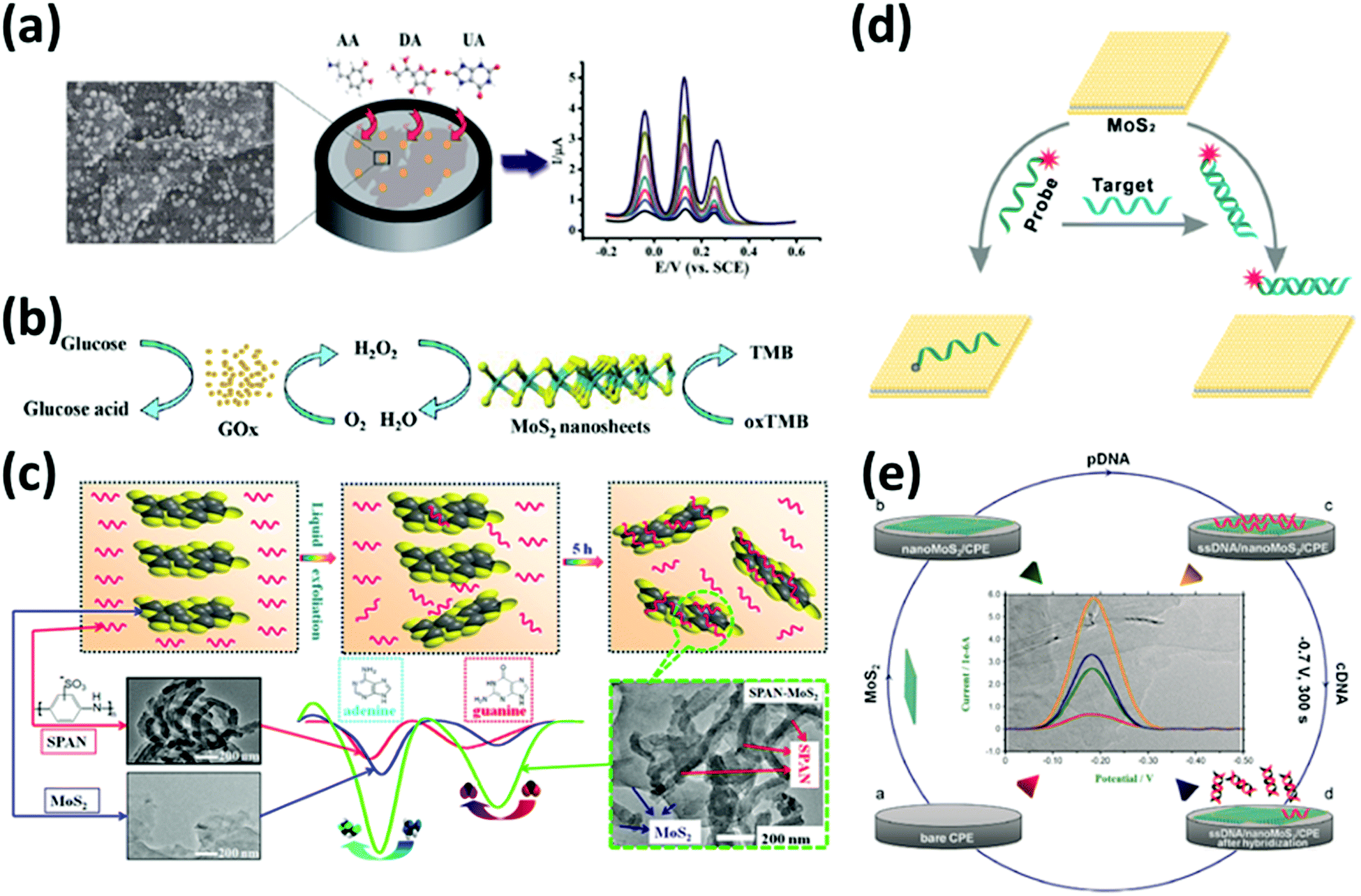 | ||
| Fig. 25 Representation of different mechanisms used for chemical detection utilizing MoS2-based materials. (a) Electrochemical sensing of ascorbic acid (AA), dopamine (DA) and uric acid (UA) with gold nanoparticle–MoS2 nanosheets. Reproduced with permission.508 Copyright 2014, Royal Society of Chemistry. (b) Sketch of catalytic reactions while colorimetric detection of glucose. Adapted from ref. 499 with permission of the Royal Society of Chemistry. (c) SPAN-MoS2 for electrochemical detection of adenine and guanine. Adapted from ref. 134 with permission of the American Chemical Society. (d) Fluorescence detection of complementary ssDNA. Adapted from ref. 99 with permission of the American Chemical Society. (e) Label-free electrochemical sensing of DNA. Adapted from ref. 489 with permission of Elsevier. | ||
Wu and co-workers presented the controllable lithiation process of MoS2 and subsequent liquid-phase exfoliation of the intercalated structure in water or ethanol. An electrochemical study of the as-prepared MoS2 nanosheets revealed a reduction peak in the CV in NaCl aqueous solution. The reduced MoS2 displayed good conductivity and a fast electron transfer rate in the most common redox systems applicable in electrochemical sensing of glucose and dopamine (DA) in the presence of ascorbic acid (AA) and uric acid (UA).486 A GCE was covered with MoS2 using 3-aminopropyltriethoxysilane (APTES) as the linking molecule. The electrode provided good peak separation and allowed to detect dopamine with linearity in the 1–50 μM range in the presence of such interferents as AA and UA. Additional functionalization of the electrode with glucose oxidase enables effective glucose detection.
Another approach for molecular detection was introduced by Huang et al.497 MoS2 nanosheets obtained via liquid-phase exfoliation in ethanol/water mixed with Ni NPs were drop-cast onto a GCE and Nafion copolymer. The as-prepared sensor exhibited amperometric response toward glucose with a detection limit as low as 0.31 μM. Such a GCE/Ni–MoS2/Nafion electrode allowed nonenzymatic detection of glucose with good reproducibility and long-term storage stability. The simultaneous detection of DA, AA and UA investigated by Sun et al. using a MoS2–Au NP decorated electrode to achieve ultrasensitive determination of the aforementioned biologically important molecules.508 The joint effect of a wide linearity range and effective electrical response yielded a sensing ability with detection limits as low as 100 μM, 0.05 μM and 10 μM for AA, DA and UA, respectively. Zhu and co-workers showed the fluorescence quenching ability of MoS2.99 Nanosheets obtained through exfoliation of bulk MoS2 using the electrochemical lithium-intercalation method were used as nanoprobes for adenosine. MoS2 supplied with probe molecules exhibits high fluorescence quenching efficiency (up to 98% compared with probe molecule intensity). Presence of adenosine restores fluorescence properties of nanoprobes and can be used for detection up to 5 μM of analyte. Another MoS2 fluorescent sensor for DNA detection was proposed by Huang et al.503 The nanosheets were prepared using a solution exfoliation method. The authors presented selective target DNA recognition via hybridization chain reactions (HCRs) with a stunning detection limit of 15 pM. Another example of using adsorption of dye-labelled ssDNA on a MoS2 surface was presented by Huang et al. Chemically exfoliated MoS2 was utilized as a biosensing platform for complementary DNA and allowed detection up to 500 pM.512 Shan et al. exploited a MoS2-based FET for glucose detection.513 The device was fabricated on a Si/SiO2 substrate with Au/Ni drain electrodes. The sensor exhibited a very fast response time (<1 s) and linearity in the 300 nM–30 mM range, which corresponds to the average glucose concentration present in the blood and therefore constitutes a potential candidate for real-time detection of glucose concentration in human blood.
Inspired by the unique device properties offered by MoS2, other TMDs (including WS2 TaS2, Ta2NiS5) have been the subject of further studies for sensing applications. The group of layered TMCs, including the chalcogenides with well-defined crystal structures, has been widely explored.502,514 Since MoS2 is known for its quenching properties, the entire group of TMDs is being considered as an effective platform for fluorescence sensing of biomolecules.501,507
Zhang et al. used single-layer TMD nanosheets as fluorescent sensors for DNA detection.501 To investigate the quenching ability of TiS2 and TaS2, the 6-carboxyfluorescein-labeled ssDNA probe and target DNA molecules were used. In both cases the dichalcogenide's fluorescence intensity was effectively quenched. TiS2 and TaS2 exhibited fast detection of complementary DNA with low limits of detection of 0.2 nM and 0.05 nM, respectively. Noteworthily, a TaS2-based nanosensor was found to be even more sensitive than MoS2 with a detection limit of 0.1 nM. Another fluorescence sensing platform based on WS2 for T4-polynucleotide kinase and its inhibitors was introduced by Ge and co-workers.132 dsDNA does not exhibit strong adsorption on WS2 sheets; yet when phosphorylated and degraded, the ssDNA binds to nanosheets as evidenced by the occurrence of fluorescence quenching. Linearity, a low limit of detection and a low signal-to-background ratio make this material promising for application in monitoring biological processes. Huang et al. developed WS2 ink by sonication-assisted liquid exfoliation in water supported by Au nanoparticles for detection of 17β-estradiol.496 An electrode was prepared by covering a GCE with WS2, then Au NPs were anchored and the ssDNA aptamer was applied for selective detection of target molecules. The as prepared electrode allowed determining 17β-estradiol at a concentration as low as 2 pM. Moreover, it was proved that only target molecules may cause such obvious current changes at concentrations in the range of 10−10 M. Tan and co-workers prepared single-layer ternary chalcogenides for fluorescence sensing of DNA.502 Microsized crystalline flakes of Ta2NiS5 were obtained via a chemical vapour transport technique from their elementary powders. Then high yield exfoliation was performed to produce a single-layered compound. Probe DNA was supplied with Texas red as fluorescent reporter that can be effetely quenched in the presence of TMDCs. Addition of complementary ssDNA results in fluorescence recovery and can be used for target DNA detection. The fluorescence could be recovered when the target ssDNA was added to form dsDNA. The fabricated sensor exhibited high sensitivity (up to 50 pM) and afforded a detection time of 10 min. Ta2NiS5 was also used as a “Capture–Release” nanosensor for detection of biological species (Fig. 26).
 | ||
| Fig. 26 (a) Scanning electron microscopy (SEM) image of Ta2NiS5 nanosheets. (b) Crystal structure of Ta2NiS5 along the b-axis. (c) Schematic representation of the quenching ability of Ta2NiS5 applied for ssDNA detection. (d) Fluorescence detection of different concentrations of target molecules in the presence of probe ssDNA. Adapted from ref. 502 with permission of American Chemical Society. | ||
4.3 (Bio)molecular sensing with TMD–graphene hybrid materials
Both TMDs and graphene exhibit a range of physico-chemical properties suitable for various electronic and sensing applications. In particular, further modifications of MoS2 and generation of hybrid materials might be used to generate composites with desired properties. The synergistic effects on the electrochemical performance of carbon-based materials with metal or metal oxides have been previously reported,515 thus suggesting the combinations of MoS2 with graphene-like structures as excellent candidates for a new class of electrochemical sensors. Electrodes made of TMC–graphene composites exhibit significant enhancement of electron transfer conductivity.516–518Huang et al. reported a MoS2–graphene composite prepared via a modified L-cysteine-assisted solution-phase method cast on a GCE to assemble an electrode.511 The composite displayed a wide electrochemical potential window (∼2.9 V in phosphate buffer), which is comparable to those of graphene-based electrodes. The as-prepared electrode was utilized for voltammetric determination of acetaminophen, exhibiting linear response in the 1–100 μM range. Moreover, the hybrid material showed good interference resistance: in the presence of other electrochemically active molecules the value of the oxidation peak current was sustained. Another electrochemical sensor composed of a MoS2–graphene nanohybrid film was developed by Zhao and co-workers.519 The GCE was embedded in a MoS2–graphene nanohybrid, resulting in significantly enhanced sensitivity towards honokiol – known in view of its antitumor and antibacterial activity used in western medicine. The electrode revealed high selectivity and stability with a spectacular limit of detection corresponding to 6.2 × 10⁻¹⁰ M. Pramoda et al. demonstrated the electrocatalytic activity of MoS2–rGO/GCE against dopamine and proved its superior nature over a bare rGO-modified electrode.520 Effective detection of DA in the presence of interferents was established at a level of 0.55 μM.
The most important parameters, including the type of sensor, limit of detection and linearity range, of TMD-based sensors are presented in Table 10.
| Material | Type of sensor | Analyte | Limit of detection | Linearity range | Ref. |
|---|---|---|---|---|---|
| List of abbreviations. NPs: nanoparticles, DA: dopamine, AA: ascorbic acid, UA: uric acid, PANI: polyaniline, TaS2: tantalum(IV) sulfide, TaNiS5: tantalum nickel sulfide, HPR: horseradish peroxidase. | |||||
| MoS2 | Electrochemical | H2O2 | 2.5 nM | 0.1–100 μM | 488 |
| DNA | 0.019 fM | 0.1–1 × 10⁵ nM | 489 | ||
| Fluorescent | DNA | 15 pM | 0–200 pM | 503 | |
| DNA | 500 pM | 0–50 nM | 512 | ||
| FET | Glucose | 300 nM | 300 nM–30 mM | 513 | |
| MoS2–Pt NPs | Electrochemical | DA | 0.17 μM | 0.5–150 μM | 495 |
| AA | 0.98 μM | 5–1000 μM | |||
| H2O2 | 1.0 μM | 4.0–48500 μM |
521 | ||
| MoS2–NiNPs | Glucose | 0.31 μM | 0–4 mM | 497 | |
| MoS2–Ag/chitosan | Tryptophan | 0.05 μM | 0.5–120 μM | 509 | |
| MoS2–Au NPs | AA | 100 μM | 1–70 mM | 508 | |
| DA | 0.05 μM | 0.05–4 × 10⁴ μM | |||
| UA | 10 μM | 10–103 μM | |||
| DA | 80 nM | 0.1–200 μM | 494 | ||
| Glucose | 2.8 μM | 10–300 μM | 493 | ||
| MoS2–PANI | Adenine | 3 nM | 0.05–100 μM | 134 | |
| Guanine | 5 nM | 0.05–100 μM | |||
| Chloramphenicol | 65 nM | 0.1–1000 μM | 498 | ||
| WS2 | Glucose | 2.9 μM | 5–300 μM | 500 | |
| WS2–Au NPs | 17β-Estradiol | 1 pM | 0.01–10 nM | 496 | |
| WS2–acetylene black | DNA | 0.12 fM | 0.001–100 pM | 522 | |
| TaS2 | Fluorescent | DNA | 0.05 nM | 0–5 nM | 501 |
| TaNiS5 | DNA | 50 pM | 0–5 nM | 502 | |
| MoS2–graphene | Electrochemical | Acetaminophen | 20 nM | 0.1–100 μM | 511 |
| Honokiol | 0.62 nM | 1.0 nM–2.5 μM | 519 | ||
| H2O2 | 1.25 μM | 6.25–225 μM | 523 | ||
| MoS2–rGO | DA | 0.94 μM | 1.5–100 μM | 520 | |
| HPR-MoS2–graphene | H2O2 | 0.049 μM | 0.2 μM–1.1 mM | 510 | |
4.4 (Bio)molecular sensing with other 2DMs
Hexagonal BN is known to be the most stable allotrope among the BN crystalline forms. A few electron transfer reactions toward biomolecule oxidation for commonly used electrodes immobilized with boron nitride have been reported and the results are comparable to those of other 2DM based sensors.524,525 However, SERS seems to be a more popular technique for the development of hBN-based chemical sensors. Noteworthily, the boron–nitrogen bonds of hBN can be used for further modifications or to facilitate the detection of organic molecules via the polarization of B–N bonds.168 Moreover, the modification of the BN surface, e.g. introducing noble metal NPs, allows the enhancement in the Raman signal, thus rendering such material a practical support for SERS. Moreover, BN exhibits a high fluorescence quenching ability and different affinities toward single stranded DNA and double stranded DNA, allowing sensitive detection of complementary DNA fragments.526Khan et al. reported the electrocatalytic behaviour of hBN toward the detection of dopamine.524 The electrode was prepared by drop-casting an ethanolic solution of crystalline hexagonal boron nitride on a screen-printed graphitic electrode (SPE) and found to determine dopamine in the presence of common interference molecules ascorbic acid (AA) and uric acid (UA). The obtained sensor exhibited a limit of detection of 0.65 μM, which is comparable to those of other 2D-based dopamine sensors. Zhan and co-workers exploited the quenching ability of boron nitride for DNA detection.526 The experiment revealed an effective fluorescence decrease of labelled ss-DNA in the presence of boron nitride nanosheets (BNNS), reaching up to 85%. This sensor exhibited a low limit of detection toward target DNA molecules (104 pM) and linearity in the 0.6–20 nM range. Lin et al. assembled a SERS-based sensor for rhodamine 6G (R6G) detection with high reusability.168 Silver-decorated boron nitride nanosheets, prepared via reduction of Ag salt in the presence of BNNS, were deposited on quartz substrates using substrate transfer techniques, resulting in a thermal-oxidation resistant material, which facilitates the removal of any residual analyte. Another SERS sensor for aromatic molecules was prepared by introduction of Au NPs onto BN nanosheets obtained using the Scotch tape technique. Cai et al. proposed substrates tested toward R6G detection, with signals greatly enhanced in the presence of 10−6 M solutions of analyte.527 The fabricated sensor also allows the effective removal of detected molecules by thermal treatment.
MXene-based sensors exhibit good electrochemical activity toward a range of biologically important molecules like glucose,528 H2O2178,529 and nitrites.179 Wang and co-workers presented a nanocomposite of TiO2 modified with Ti3C2MXene encapsulating haemoglobin with effective activity toward H2O2 detection.529 TiO2–Ti3C2 was synthesized in an autoclave, then a mixture consisting of a suspension of the nanocomposite, haemoglobin in phosphate buffered saline (PBS) and Nafion were applied on a GCE by a simple casting method. The obtained MXene enzyme-based sensor exhibited efficient electrochemical performance, allowing determination of hydrogen peroxide with a low limit of detection of 14 nM and a wide linear range of 0.1–380 μM. Another Ti3C2-based electrochemical sensor supplied with haemoglobin to provide direct electron transfer was realized by Liu et al.179 This sensor, due to its large surface area and high conductivity, displayed good electrochemical performance, allowing detection of sodium nitrite (NaNO2) with a linear range of 0.5–11800 μM and a limit of detection equal to 0.12 μM. Rakhi and co-workers used the synergistic effect of Au NPs and MXenes on glucose oxidation.528 Two-dimensional titanium carbide was obtained via exfoliation of Ti3AlC2. Further sonication of MXenes with Au NPs resulted in Au/MXene composites used to prepare electrodes together with glucose oxidase (GOx) by casting the obtained mixtures onto GCEs. These sensors displayed a detection limit of glucose up to 5.9 μM and amperometric response with linearity in the 0.1 mM to 18 mM range.
Two-dimensional nanosheets of black phosphorus have gained attention as an analogue of other widely explored layered materials. BP exhibits impressive opto-electronic properties but it is particularly sensitive to water and oxygen; thus during the preparation of BP-based chemical sensors, particular precautions have to be taken.530,531 Yan and co-workers proposed a nonenzymatic sensor based on solvent exfoliated BP for determination of H2O2.530 Few-layered black phosphorus, produced via a supercritical carbon dioxide-assisted synthesis, was used for electrode preparation by casting an ethanolic solution onto a GCE. The electrochemical impedance was investigated in N2-saturated phosphate buffered saline (PBS) exhibiting linearity in the 1 × 10⁻⁷ M to 1 × 10⁻⁵ M range with a limit of detection as low as 1 × 10⁻⁷ M. Yew et al. used higher affinity of BP NPs toward ssDNA and prepared a fluorescent sensor for nucleic acid detection.531 This biosensing platform provided linearity in the 4–4000 pM range and a limit of detection equal to 5.9 pM.
The performances of hBN, MXenes and BP-based materials as (bio)molecular sensors are summarized in Table 11.
| Material | Type of sensor | Analyte | Limit of detection | Linearity range | Ref. |
|---|---|---|---|---|---|
| List of abbreviations. DA: dopamine, BNNS: boron nitride nanosheets, SERS: surface enhanced Raman scattering, R6G: rhodamine 6G, GOx: glucose oxidase, BPNPs: black phosphorus nanoparticles. | |||||
| hBN | Electrochemical | DA | 0.65 μM | — | 524 |
| Surfactant exfoliated hBN | 1.57 μM | — | 525 | ||
| BNNS | Fluorescent | DNA | 104 pM | 0.6–20 nM | 526 |
| Ag–BNNS | SERS | R6G | 10 μM | — | 168 |
| Au/BN | 1 μM | — | 527 | ||
| TiO2–Ti3C2 | Electrochemical | H2O2 | 14 nM | 0.1–380 μM | 529 |
| Ti3C2 | NaNO2 | 0.12 μM | 0.5–11800 μM |
179 | |
| GOx–Au–MXene | Glucose | 5.9 μM | 0.1–18 mM | 528 | |
| BP | H2O2 | 0.1 μM | 0.1–10 μM | 530 | |
| BPNPs | Fluorescent | DNA | 5.9 pM | 4–4000 pM | 531 |
In this section we have discussed 2DMs and 2DM-based composites for the sensing of (bio)molecular species. A range of unique physico-chemical properties offered by 2DMs allows fabrication of various types of chemical sensors including fluorescent, electrochemical, FET and SERS sensors. The recent literature includes investigations of the most important biological molecules with particular attention to molecules relevant to medical sciences. Among various advantages of 2DM based sensors the extremely low limit of detection (reaching the picomolar level), ultrafast detection (<1 s) and wide linearity of response signals should be emphasized. Moreover, most of the 2DM based sensors exhibit high selectivity and allow determination of multiple target molecules even in the presence of common interferents. The possibility of further modifications of 2DMs allows achieving multicomponent systems, offering better performances in the effective determination of target analytes. Noteworthily, the spectrum of molecules detectable with presented sensors is quite narrow. Also there are a few issues that should be considered while developing new sensing materials such as stability, reusability and biocompatibility. Electrochemical sensing seems to be one of the most widespread approaches applied in chemical sensing, which affirms the superior electrical properties of graphene and TMDs. In the case of TMDs recent investigations seem to be mainly focused on MoS2 and WS2, while the other representatives have not gathered much attention so far. Notably, the group of novel 2DMs such as hBN, MXenes and BP holds great potential in molecular sensing. Basing on few recent reports those materials constitute promising fundaments for further investigations in terms of their sensing properties.
5 Conclusions and outlook
Alongside the numerous extraordinary physical and chemical properties exhibited by 2DMs, their high surface area-to-volume ratios represent a key additional advantage for applications in sensing. The all-surface-and-volume-free character guarantees the highest sensitivity to any changes in 2DMs’ environments, which is an absolute prerequisite for the development of high-performance sensing devices. However, the use of pristine, defect free sheets may result in weak and unspecific interactions with the chosen analytes. Defects hold a pivotal role in 2DMs: they allow the modulation of the (opto)electronic properties, and in particular the engineering of the band gap, which plays a crucial role in improving the sensitivity of the device. Moreover, the presence of dangling groups on the surface can promote analyte absorption, consequently yielding an improvement in the sensing performances. Furthermore, the presence of defects highly increases the chemical reactivity of 2DMs, enabling further chemical functionalization of the reactive sites, which may result in high specificity, enhanced sensitivity and a low detection limit towards the targeted analyte. On the other hand, a lack of control during defect engineering can result in irreproducible properties of 2DMs. In particular, the increased reactivity and the presence of dangling bonds with different chemical structures on the basal plane (or edges) of the 2DM may result in an enhanced, yet, unselective binding of the analytes, ultimately leading to poor selectivity, long response or an even incomplete recovery time of the sensor.One of the greatest challenges to be tackled in the near future is the controlled introduction of ad hoc defects in 2DMs with a precise spatial resolution and concentration. Ideally, the chemical composition of the defects has to be complemented by a chemical functionalization of the reactive sites with the receptor of the analyte of choice. Such a strategy needs to be pursued by mastering the principles of molecular recognitions, e.g. via tailoring of supramolecular interactions, which may result not only in ultrasensitive 2DMs but also in superior selectivity and response times – making the actual step towards industrial products. Additionally, chemical programmability, through the generation of multicomponent assemblies based on 2DMs, may enable the future development of multianalyte sensing. Although optical sensors based on the change in the photoluminescence properties of 2DMs upon interaction with analytes have been widely and successfully employed for both metals and biologically relevant molecules, electrochemical sensors seem to be the most promising since they provide a direct electrical response without the need for employing a transducer. By taking advantage not only of the superior electrical properties of graphene and other 2DMs, but also of their excellent mechanical properties such as robustness and flexibility, 2DM based sensors can be supported on flexible foils, for smart wearable technologies for monitoring the human/environment interface. Interestingly, the recent demonstration of the compatibility of 2DMs with “on-the-skin” applications opens the door towards their use for the detection of clinically relevant biomarkers. Such 2DM-based tattoos may therefore find application as dry on-the-skin sensors characterized by low susceptibility to motion artefacts, which is one of the biggest drawbacks of conventional dry sensors and electrodes for point-of-care health monitoring.
Conflicts of interest
There are no conflicts to declare.Acknowledgements
This work was supported by the European Commission through the Graphene Flagship Core 1 project (GA-696656) and the Polish National Science Centre (Grant No. 2015/18/E/ST5/00188). We also are thankful for the support of the Agence Nationale de la Recherche through the LabEx project Chemistry of Complex Systems (ANR-10-LABX-0026_CSC), and the International Center for Frontier Research in Chemistry (icFRC). D. P. acknowledges the support from the Embassy of France in Poland in the form of a scholarship at the Institut de Science et d'Ingénierie Supramoléculaires, University of Strasbourg.References
- K. S. Novoselov, A. K. Geim, S. V. Morozov, D. Jiang, M. I. Katsnelson, I. V. Grigorieva, S. V. Dubonos and A. A. Firsov, Nature, 2005, 438, 197 CrossRef PubMed.
- A. C. Ferrari, F. Bonaccorso, V. Fal'ko, K. S. Novoselov, S. Roche, P. Boggild, S. Borini, F. H. L. Koppens, V. Palermo, N. Pugno, J. A. Garrido, R. Sordan, A. Bianco, L. Ballerini, M. Prato, E. Lidorikis, J. Kivioja, C. Marinelli, T. Ryhanen, A. Morpurgo, J. N. Coleman, V. Nicolosi, L. Colombo, A. Fert, M. Garcia-Hernandez, A. Bachtold, G. F. Schneider, F. Guinea, C. Dekker, M. Barbone, Z. Sun, C. Galiotis, A. N. Grigorenko, G. Konstantatos, A. Kis, M. Katsnelson, L. Vandersypen, A. Loiseau, V. Morandi, D. Neumaier, E. Treossi, V. Pellegrini, M. Polini, A. Tredicucci, G. M. Williams, B. Hee Hong, J.-H. Ahn, J. Min Kim, H. Zirath, B. J. van Wees, H. van der Zant, L. Occhipinti, A. Di Matteo, I. A. Kinloch, T. Seyller, E. Quesnel, X. Feng, K. Teo, N. Rupesinghe, P. Hakonen, S. R. T. Neil, Q. Tannock, T. Lofwander and J. Kinaret, Nanoscale, 2015, 7, 4598 RSC.
- Q. H. Wang, K. Kalantar-Zadeh, A. Kis, J. N. Coleman and M. S. Strano, Nat. Nanotechnol., 2012, 7, 699 CrossRef PubMed.
- M. W. Barsoum, Prog. Solid State Chem., 2000, 28, 201 CrossRef.
- L. Li, Y. Yu, G. J. Ye, Q. Ge, X. Ou, H. Wu, D. Feng, X. H. Chen and Y. Zhang, Nat. Nanotechnol., 2014, 9, 372 CrossRef PubMed.
- S. P. Koenig, R. A. Doganov, H. Schmidt, A. H. Castro Neto and B. Özyilmaz, Appl. Phys. Lett., 2014, 104, 103106 CrossRef.
- H. Liu, A. T. Neal, Z. Zhu, Z. Luo, X. Xu, D. Tománek and P. D. Ye, ACS Nano, 2014, 8, 4033 CrossRef PubMed.
- A. Gupta, T. Sakthivel and S. Seal, Prog. Mater. Sci., 2015, 73, 44 CrossRef.
- A. S. Mayorov, R. V. Gorbachev, S. V. Morozov, L. Britnell, R. Jalil, L. A. Ponomarenko, P. Blake, K. S. Novoselov, K. Watanabe, T. Taniguchi and A. K. Geim, Nano Lett., 2011, 11, 2396 CrossRef PubMed.
- D. C. Elias, R. V. Gorbachev, A. S. Mayorov, S. V. Morozov, A. A. Zhukov, P. Blake, L. A. Ponomarenko, I. V. Grigorieva, K. S. Novoselov, F. Guinea and A. K. Geim, Nat. Phys., 2011, 7, 701 Search PubMed.
- A. Kuc, N. Zibouche and T. Heine, Phys. Rev. B: Condens. Matter Mater. Phys., 2011, 83, 245213 CrossRef.
- A. Splendiani, L. Sun, Y. Zhang, T. Li, J. Kim, C.-Y. Chim, G. Galli and F. Wang, Nano Lett., 2010, 10, 1271 CrossRef PubMed.
- J.-S. Kim, H.-W. Yoo, H. O. Choi and H.-T. Jung, Nano Lett., 2014, 14, 5941 CrossRef PubMed.
- D. J. Late, Y.-K. Huang, B. Liu, J. Acharya, S. N. Shirodkar, J. Luo, A. Yan, D. Charles, U. V. Waghmare, V. P. Dravid and C. N. R. Rao, ACS Nano, 2013, 7, 4879 CrossRef PubMed.
- K. Kalantar-zadeh and J. Z. Ou, ACS Sens., 2016, 1, 5 CrossRef.
- Y. Song, Y. Luo, C. Zhu, H. Li, D. Du and Y. Lin, Biosens. Bioelectron., 2016, 76, 195 CrossRef PubMed.
- V. Georgakilas, M. Otyepka, A. B. Bourlinos, V. Chandra, N. Kim, K. C. Kemp, P. Hobza, R. Zboril and K. S. Kim, Chem. Rev., 2012, 112, 6156 CrossRef PubMed.
- B. Cai, S. Zhang, Z. Yan and H. Zeng, ChemNanoMat, 2015, 1, 542 CrossRef.
- E. A. Meyer, R. K. Castellano and F. Diederich, Angew. Chem., Int. Ed., 2003, 42, 1210 CrossRef PubMed.
- S. K. Burley and G. A. Petsko, FEBS Lett., 1986, 203, 139 CrossRef PubMed.
- P. Tarakeshwar, K. S. Kim, E. Kraka and D. Cremer, J. Chem. Phys., 2001, 115, 6018 CrossRef.
- E. C. Lee, B. H. Hong, J. Y. Lee, J. C. Kim, D. Kim, Y. Kim, P. Tarakeshwar and K. S. Kim, J. Am. Chem. Soc., 2005, 127, 4530 CrossRef PubMed.
- S. J. Grabowski, J. Phys. Chem. A, 2001, 105, 10739 CrossRef.
- P. Tarakeshwar, H. S. Choi and K. S. Kim, J. Am. Chem. Soc., 2001, 123, 3323 CrossRef PubMed.
- E.-I. Kim, S. Paliwal and C. S. Wilcox, J. Am. Chem. Soc., 1998, 120, 11192 CrossRef.
- K. E. Riley, M. Pitoňák, P. Jurečka and P. Hobza, Chem. Rev., 2010, 110, 5023 CrossRef PubMed.
- C. A. Hunter and J. K. M. Sanders, J. Am. Chem. Soc., 1990, 112, 5525 CrossRef.
- C. A. Hunter, Chem. Soc. Rev., 1994, 23, 101 RSC.
- E. C. Lee, D. Kim, P. Jurečka, P. Tarakeshwar, P. Hobza and K. S. Kim, J. Phys. Chem. A, 2007, 111, 3446 CrossRef PubMed.
- I. Geronimo, E. C. Lee, N. J. Singh and K. S. Kim, J. Chem. Theory Comput., 2010, 6, 1931 CrossRef PubMed.
- W. Wang and P. Hobza, ChemPhysChem, 2008, 9, 1003 CrossRef PubMed.
- D. A. Dougherty and D. A. Stauffer, Science, 1990, 250, 1558 CrossRef PubMed.
- D. Kim, S. Hu, P. Tarakeshwar, K. S. Kim and J. M. Lisy, J. Phys. Chem. A, 2003, 107, 1228 CrossRef.
- S. Tsuzuki, M. Yoshida, T. Uchimaru and M. Mikami, J. Phys. Chem. A, 2001, 105, 769 CrossRef.
- S. E. Wheeler and K. N. Houk, J. Am. Chem. Soc., 2009, 131, 3126 CrossRef PubMed.
- M. A. Gebbie, W. Wei, A. M. Schrader, T. R. Cristiani, H. A. Dobbs, M. Idso, B. F. Chmelka, J. H. Waite and J. N. Israelachvili, Nat. Chem., 2017, 9, 473 CrossRef PubMed.
- A. S. Mahadevi and G. N. Sastry, Chem. Rev., 2013, 113, 2100 CrossRef PubMed.
- P. B. Crowley and A. Golovin, Proteins: Struct., Funct., Bioinf., 2005, 59, 231 CrossRef PubMed.
- J. P. Gallivan and D. A. Dougherty, Proc. Natl. Acad. Sci. U. S. A., 1999, 96, 9459 CrossRef.
- K. S. Kim, P. Tarakeshwar and J. Y. Lee, Chem. Rev., 2000, 100, 4145 CrossRef PubMed.
- D. Quiñonero, C. Garau, C. Rotger, A. Frontera, P. Ballester, A. Costa and P. M. Deyà, Angew. Chem., Int. Ed., 2002, 41, 3389 CrossRef.
- B. L. Schottel, H. T. Chifotides and K. R. Dunbar, Chem. Soc. Rev., 2008, 37, 68 RSC.
- Y. S. Rosokha, S. V. Lindeman, S. V. Rosokha and J. K. Kochi, Angew. Chem., Int. Ed., 2004, 43, 4650 CrossRef PubMed.
- P. De Hoog, P. Gamez, I. Mutikainen, U. Turpeinen and J. Reedijk, Angew. Chem., Int. Ed., 2004, 116, 5815 CrossRef PubMed.
- R. E. Dawson, A. Hennig, D. P. Weimann, D. Emery, V. Ravikumar, J. Montenegro, T. Takeuchi, S. Gabutti, M. Mayor, J. Mareda, C. A. Schalley and S. Matile, Nat. Chem., 2010, 2, 533 CrossRef PubMed.
- A. Frontera, P. Gamez, M. Mascal, T. J. Mooibroek and J. Reedijk, Angew. Chem., Int. Ed., 2011, 50, 9564 CrossRef PubMed.
- B. L. Schottel, H. T. Chifotides, M. Shatruk, A. Chouai, L. M. Pérez, J. Bacsa and K. R. Dunbar, J. Am. Chem. Soc., 2006, 128, 5895 CrossRef PubMed.
- H. T. Chifotides and K. R. Dunbar, Acc. Chem. Res., 2013, 46, 894 CrossRef PubMed.
- C. Garau, A. Frontera, D. Quiñonero, P. Ballester, A. Costa and P. M. Deyà, J. Phys. Chem. A, 2004, 108, 9423 CrossRef.
- D. Kim, P. Tarakeshwar and K. S. Kim, J. Phys. Chem. A, 2004, 108, 1250 CrossRef.
- P. G. Moses, J. J. Mortensen, B. I. Lundqvist and J. K. Nørskov, J. Chem. Phys., 2009, 130, 104709 CrossRef PubMed.
- N. Huo, S. Yang, Z. Wei, S. S. Li, J. B. Xia and J. Li, Sci. Rep., 2014, 4, 5209 CrossRef PubMed.
- A. Hashimoto, K. Suenaga, A. Gloter, K. Urita and S. Iijima, Nature, 2004, 430, 870 CrossRef PubMed.
- W. Zhou, X. Zou, S. Najmaei, Z. Liu, Y. Shi, J. Kong, J. Lou, P. M. Ajayan, B. I. Yakobson and J.-C. Idrobo, Nano Lett., 2013, 13, 2615 CrossRef PubMed.
- F. Banhart, J. Kotakoski and A. V. Krasheninnikov, ACS Nano, 2011, 5, 26 CrossRef PubMed.
- L. G. Cançado, A. Jorio, E. H. M. Ferreira, F. Stavale, C. A. Achete, R. B. Capaz, M. V. O. Moutinho, A. Lombardo, T. S. Kulmala and A. C. Ferrari, Nano Lett., 2011, 11, 3190 CrossRef PubMed.
- S. Feng, Z. Lin, X. Gan, R. Lv and M. Terrones, Nanoscale Horiz., 2017, 2, 72 RSC.
- A. Ambrosi and M. Pumera, Chem. – Eur. J., 2010, 16, 10946 CrossRef PubMed.
- K. C. Santosh, C. L. Roberto, A. Rafik, M. W. Robert and C. Kyeongjae, Nanotechnology, 2014, 25, 375703 CrossRef PubMed.
- D. Liu, Y. Guo, L. Fang and J. Robertson, Appl. Phys. Lett., 2013, 103, 183113 CrossRef.
- S. Tongay, J. Suh, C. Ataca, W. Fan, A. Luce, J. S. Kang, J. Liu, C. Ko, R. Raghunathanan, J. Zhou, F. Ogletree, J. Li, J. C. Grossman and J. Wu, Sci. Rep., 2013, 3, 2657 CrossRef PubMed.
- H. Nan, Z. Wang, W. Wang, Z. Liang, Y. Lu, Q. Chen, D. He, P. Tan, F. Miao, X. Wang, J. Wang and Z. Ni, ACS Nano, 2014, 8, 5738 CrossRef PubMed.
- J. Xie, H. Zhang, S. Li, R. Wang, X. Sun, M. Zhou, J. Zhou, X. W. Lou and Y. Xie, Adv. Mater., 2013, 25, 5807 CrossRef PubMed.
- L. Rodriguez-Perez, M. a. A. Herranz and N. Martin, Chem. Commun., 2013, 49, 3721 RSC.
- G. L. C. Paulus, Q. H. Wang and M. S. Strano, Acc. Chem. Res., 2013, 46, 160 CrossRef PubMed.
- S. Niyogi, E. Bekyarova, M. E. Itkis, H. Zhang, K. Shepperd, J. Hicks, M. Sprinkle, C. Berger, C. N. Lau, W. A. de Heer, E. H. Conrad and R. C. Haddon, Nano Lett., 2010, 10, 4061 CrossRef PubMed.
- J. M. Englert, C. Dotzer, G. Yang, M. Schmid, C. Papp, J. M. Gottfried, H.-P. Steinrück, E. Spiecker, F. Hauke and A. Hirsch, Nat. Chem., 2011, 3, 279 CrossRef PubMed.
- H. Liu, S. Ryu, Z. Chen, M. L. Steigerwald, C. Nuckolls and L. E. Brus, J. Am. Chem. Soc., 2009, 131, 17099 CrossRef PubMed.
- M. Quintana, K. Spyrou, M. Grzelczak, W. R. Browne, P. Rudolf and M. Prato, ACS Nano, 2010, 4, 3527 CrossRef PubMed.
- D. Chen, H. Feng and J. Li, Chem. Rev., 2012, 112, 6027 CrossRef PubMed.
- D. R. Dreyer, S. Park, C. W. Bielawski and R. S. Ruoff, Chem. Soc. Rev., 2010, 39, 228 RSC.
- M. Zhou, Y. Zhai and S. Dong, Anal. Chem., 2009, 81, 5603 CrossRef PubMed.
- J. T. Robinson, F. K. Perkins, E. S. Snow, Z. Wei and P. E. Sheehan, Nano Lett., 2008, 8, 3137 CrossRef PubMed.
- S. Wu, Q. He, C. Tan, Y. Wang and H. Zhang, Small, 2013, 9, 1160 CrossRef PubMed.
- W. Yuan and G. Shi, J. Mater. Chem. A, 2013, 1, 10078 RSC.
- Q. He, S. Wu, Z. Yin and H. Zhang, Chem. Sci., 2012, 3, 1764 RSC.
- G. Zhao, J. Li, X. Ren, C. Chen and X. Wang, Environ. Sci. Technol., 2011, 45, 10454 CrossRef PubMed.
- R. Sitko, E. Turek, B. Zawisza, E. Malicka, E. Talik, J. Heimann, A. Gagor, B. Feist and R. Wrzalik, Dalton Trans., 2013, 42, 5682 RSC.
- G. Eda and M. Chhowalla, Adv. Mater., 2010, 22, 2392 CrossRef PubMed.
- G. Ko, H. Y. Kim, J. Ahn, Y. M. Park, K. Y. Lee and J. Kim, Curr. Appl. Phys., 2010, 10, 1002 CrossRef.
- D. R. Dreyer, A. D. Todd and C. W. Bielawski, Chem. Soc. Rev., 2014, 43, 5288 RSC.
- S. Eigler and A. Hirsch, Angew. Chem., Int. Ed., 2014, 53, 7720 CrossRef PubMed.
- C. K. Chua and M. Pumera, Chem. Soc. Rev., 2014, 43, 291 RSC.
- L. Zhou, B. He, Y. Yang and Y. He, RSC Adv., 2014, 4, 32570 RSC.
- C. Tsai, H. Li, S. Park, J. Park, H. S. Han, J. K. Nørskov, X. Zheng and F. Abild-Pedersen, Nat. Commun., 2017, 8, 15113 CrossRef PubMed.
- S. Bertolazzi, S. Bonacchi, G. Nan, A. Pershin, D. Beljonne and P. Samorì, Adv. Mater., 2017, 29, 1606760 CrossRef PubMed.
- K. Cho, M. Min, T.-Y. Kim, H. Jeong, J. Pak, J.-K. Kim, J. Jang, S. J. Yun, Y. H. Lee, W.-K. Hong and T. Lee, ACS Nano, 2015, 9, 8044 CrossRef PubMed.
- E. P. Nguyen, B. J. Carey, J. Z. Ou, J. van Embden, E. D. Gaspera, A. F. Chrimes, M. J. S. Spencer, S. Zhuiykov, K. Kalantar-zadeh and T. Daeneke, Adv. Mater., 2015, 27, 6225 CrossRef PubMed.
- A. Aliprandi, D. Pakulski, A. Ciesielski and P. Samorì, ACS Nano, 2017, 11, 10654 CrossRef PubMed.
- B. M. Venkatesan and R. Bashir, Nat. Nanotechnol., 2011, 6, 615 CrossRef PubMed.
- S. Garaj, W. Hubbard, A. Reina, J. Kong, D. Branton and J. A. Golovchenko, Nature, 2010, 467, 190 CrossRef PubMed.
- S. Mao, J. Chang, H. Pu, G. Lu, Q. He, H. Zhang and J. Chen, Chem. Soc. Rev., 2017, 46, 6872 RSC.
- Y. Liu, X. Dong and P. Chen, Chem. Soc. Rev., 2012, 41, 2283 RSC.
- D. Chen, L. Tang and J. Li, Chem. Soc. Rev., 2010, 39, 3157 RSC.
- M. J. Allen, V. C. Tung and R. B. Kaner, Chem. Rev., 2010, 110, 132 CrossRef PubMed.
- S. Cui, H. Pu, S. A. Wells, Z. Wen, S. Mao, J. Chang, M. C. Hersam and J. Chen, Nat. Commun., 2015, 6, 8632 CrossRef PubMed.
- Y. Wang, Z. Li, J. Wang, J. Li and Y. Lin, Trends Biotechnol., 2011, 29, 205 CrossRef PubMed.
- Z. Tang, H. Wu, J. R. Cort, G. W. Buchko, Y. Zhang, Y. Shao, I. A. Aksay, J. Liu and Y. Lin, Small, 2010, 6, 1205 CrossRef PubMed.
- C. Zhu, Z. Zeng, H. Li, F. Li, C. Fan and H. Zhang, J. Am. Chem. Soc., 2013, 135, 5998 CrossRef PubMed.
- D. Dinda, A. Gupta, B. K. Shaw, S. Sadhu and S. K. Saha, ACS Appl. Mater. Interfaces, 2014, 6, 10722 CrossRef PubMed.
- X. Ling, L. Xie, Y. Fang, H. Xu, H. Zhang, J. Kong, M. S. Dresselhaus, J. Zhang and Z. Liu, Nano Lett., 2010, 10, 553 CrossRef PubMed.
- X. Ling, W. Fang, Y.-H. Lee, P. T. Araujo, X. Zhang, J. F. Rodriguez-Nieva, Y. Lin, J. Zhang, J. Kong and M. S. Dresselhaus, Nano Lett., 2014, 14, 3033 CrossRef PubMed.
- S. Schlücker, Angew. Chem., Int. Ed., 2014, 53, 4756 CrossRef PubMed.
- S. Laing, L. E. Jamieson, K. Faulds and D. Graham, Nat. Rev. Chem., 2017, 1, 0060 CrossRef.
- A.-I. Henry, B. Sharma, M. F. Cardinal, D. Kurouski and R. P. Van Duyne, Anal. Chem., 2016, 88, 6638 CrossRef PubMed.
- M. F. Cardinal, E. Vander Ende, R. A. Hackler, M. O. McAnally, P. C. Stair, G. C. Schatz and R. P. Van Duyne, Chem. Soc. Rev., 2017, 46, 3886 RSC.
- S. Nie and S. R. Emory, Science, 1997, 275, 1102 CrossRef PubMed.
- K. Kneipp, Y. Wang, H. Kneipp, L. T. Perelman, I. Itzkan, R. R. Dasari and M. S. Feld, Phys. Rev. Lett., 1997, 78, 1667 CrossRef.
- L. Sun, H. Hu, D. Zhan, J. Yan, L. Liu, J. S. Teguh, E. K. L. Yeow, P. S. Lee and Z. Shen, Small, 2014, 10, 1090 CrossRef PubMed.
- X. Ling, S. Huang, S. Deng, N. Mao, J. Kong, M. S. Dresselhaus and J. Zhang, Acc. Chem. Res., 2015, 48, 1862 CrossRef PubMed.
- A. J. Bandodkar, I. Jeerapan and J. Wang, ACS Sens., 2016, 1, 464 CrossRef.
- E. Singh, M. Meyyappan and H. S. Nalwa, ACS Appl. Mater. Interfaces, 2017, 9, 34544 CrossRef PubMed.
- H. Lee, T. K. Choi, Y. B. Lee, H. R. Cho, R. Ghaffari, L. Wang, H. J. Choi, T. D. Chung, N. Lu, T. Hyeon, S. H. Choi and D.-H. Kim, Nat. Nanotechnol., 2016, 11, 566 CrossRef PubMed.
- N. O. Weiss, H. Zhou, L. Liao, Y. Liu, S. Jiang, Y. Huang and X. Duan, Adv. Mater., 2012, 24, 5782 CrossRef PubMed.
- V. Berry, Carbon, 2013, 62, 1 CrossRef.
- F. Guo, G. Silverberg, S. Bowers, S.-P. Kim, D. Datta, V. Shenoy and R. H. Hurt, Environ. Sci. Technol., 2012, 46, 7717 CrossRef PubMed.
- D. Pierleoni, Z. Y. Xia, M. Christian, S. Ligi, M. Minelli, V. Morandi, F. Doghieri and V. Palermo, Carbon, 2016, 96, 503 CrossRef.
- D. Prasai, J. C. Tuberquia, R. R. Harl, G. K. Jennings and K. I. Bolotin, ACS Nano, 2012, 6, 1102 CrossRef PubMed.
- A. K. Geim, Science, 2009, 324, 1530 CrossRef PubMed.
- X. Li, W. Cai, J. An, S. Kim, J. Nah, D. Yang, R. Piner, A. Velamakanni, I. Jung, E. Tutuc, S. K. Banerjee, L. Colombo and R. S. Ruoff, Science, 2009, 324, 1312 CrossRef PubMed.
- Y. Zhang, L. Zhang and C. Zhou, Acc. Chem. Res., 2013, 46, 2329 CrossRef PubMed.
- C. Berger, Z. M. Song, T. B. Li, X. B. Li, A. Y. Ogbazghi, R. Feng, Z. T. Dai, A. N. Marchenkov, E. H. Conrad, P. N. First and W. A. de Heer, J. Phys. Chem. B, 2004, 108, 19912 CrossRef.
- Y. Zhu, S. Murali, W. Cai, X. Li, J. W. Suk, J. R. Potts and R. S. Ruoff, Adv. Mater., 2010, 22, 3906 CrossRef PubMed.
- S. Basu and P. Bhattacharyya, Sens. Actuators, B, 2012, 173, 1 CrossRef.
- Y. Hernandez, V. Nicolosi, M. Lotya, F. M. Blighe, Z. Sun, S. De, I. T. McGovern, B. Holland, M. Byrne, Y. K. Gun'Ko, J. J. Boland, P. Niraj, G. S. Duesberg, S. Krishnamurthy, R. Goodhue, J. Hutchison, V. Scardaci, A. C. Ferrari and J. N. Coleman, Nat. Nanotechnol., 2008, 3, 563 CrossRef PubMed.
- A. Ciesielski and P. Samorì, Adv. Mater., 2016, 28, 6030 CrossRef PubMed.
- K. R. Paton, E. Varrla, C. Backes, R. J. Smith, U. Khan, A. O’Neill, C. Boland, M. Lotya, O. M. Istrate, P. King, T. Higgins, S. Barwich, P. May, P. Puczkarski, I. Ahmed, M. Moebius, H. Pettersson, E. Long, J. Coelho, S. E. O’Brien, E. K. McGuire, B. M. Sanchez, G. S. Duesberg, N. McEvoy, T. J. Pennycook, C. Downing, A. Crossley, V. Nicolosi and J. N. Coleman, Nat. Mater., 2014, 13, 624 CrossRef PubMed.
- M. Eredia, S. Bertolazzi, T. Leydecker, M. El Garah, I. Janica, G. Melinte, O. Ersen, A. Ciesielski and P. Samorì, J. Phys. Chem. Lett., 2017, 8, 3347 CrossRef PubMed.
- Z. Yin, H. Li, H. Li, L. Jiang, Y. Shi, Y. Sun, G. Lu, Q. Zhang, X. Chen and H. Zhang, ACS Nano, 2012, 6, 74 CrossRef PubMed.
- W. Wu, L. Wang, Y. Li, F. Zhang, L. Lin, S. Niu, D. Chenet, X. Zhang, Y. Hao, T. F. Heinz, J. Hone and Z. L. Wang, Nature, 2014, 514, 470 CrossRef PubMed.
- Y. Sun, S. Gao and Y. Xie, Chem. Soc. Rev., 2014, 43, 530 RSC.
- G. Zhang, G. Proni, S. Zhao, E. C. Constable, C. E. Housecroft, M. Neuburger and J. A. Zampese, Dalton Trans., 2014, 43, 12313 RSC.
- Kenry, A. Geldert, X. Zhang, H. Zhang and C. T. Lim, ACS Sens., 2016, 1, 1315 CrossRef.
- T. Yang, R. Yang, H. Chen, F. Nan, T. Ge and K. Jiao, ACS Appl. Mater. Interfaces, 2015, 7, 2867 CrossRef PubMed.
- M. Chhowalla, H. S. Shin, G. Eda, L.-J. Li, K. P. Loh and H. Zhang, Nat. Chem., 2013, 5, 263 CrossRef PubMed.
- Y. Li, K.-A. N. Duerloo, K. Wauson and E. J. Reed, Nat. Commun., 2016, 7, 10671 CrossRef PubMed.
- J. N. Coleman, M. Lotya, A. O’Neill, S. D. Bergin, P. J. King, U. Khan, K. Young, A. Gaucher, S. De, R. J. Smith, I. V. Shvets, S. K. Arora, G. Stanton, H.-Y. Kim, K. Lee, G. T. Kim, G. S. Duesberg, T. Hallam, J. J. Boland, J. J. Wang, J. F. Donegan, J. C. Grunlan, G. Moriarty, A. Shmeliov, R. J. Nicholls, J. M. Perkins, E. M. Grieveson, K. Theuwissen, D. W. McComb, P. D. Nellist and V. Nicolosi, Science, 2011, 331, 568 CrossRef PubMed.
- D. Kong, H. Wang, J. J. Cha, M. Pasta, K. J. Koski, J. Yao and Y. Cui, Nano Lett., 2013, 13, 1341 CrossRef PubMed.
- J. Shi, D. Ma, G.-F. Han, Y. Zhang, Q. Ji, T. Gao, J. Sun, X. Song, C. Li, Y. Zhang, X.-Y. Lang, Y. Zhang and Z. Liu, ACS Nano, 2014, 8, 10196 CrossRef PubMed.
- H. S. S. Ramakrishna Matte, A. Gomathi, A. K. Manna, D. J. Late, R. Datta, S. K. Pati and C. N. R. Rao, Angew. Chem., Int. Ed., 2010, 49, 4059 CrossRef PubMed.
- Z. Zeng, Z. Yin, X. Huang, H. Li, Q. He, G. Lu, F. Boey and H. Zhang, Angew. Chem., Int. Ed., 2011, 50, 11093 CrossRef PubMed.
- V. Nicolosi, M. Chhowalla, M. G. Kanatzidis, M. S. Strano and J. N. Coleman, Science, 2013, 340, 1226419 CrossRef.
- Y.-H. Lee, X.-Q. Zhang, W. Zhang, M.-T. Chang, C.-T. Lin, K.-D. Chang, Y.-C. Yu, J. T.-W. Wang, C.-S. Chang, L.-J. Li and T.-W. Lin, Adv. Mater., 2012, 24, 2320 CrossRef PubMed.
- B. Liu, L. Chen, G. Liu, A. N. Abbas, M. Fathi and C. Zhou, ACS Nano, 2014, 8, 5304 CrossRef PubMed.
- K. Lee, R. Gatensby, N. McEvoy, T. Hallam and G. S. Duesberg, Adv. Mater., 2013, 25, 6699 CrossRef PubMed.
- B. Cho, A. R. Kim, Y. Park, J. Yoon, Y. J. Lee, S. Lee, T. J. Yoo, C. G. Kang, B. H. Lee, H. C. Ko, D. H. Kim and M. G. Hahm, ACS Appl. Mater. Interfaces, 2015, 7, 2952 CrossRef PubMed.
- S.-Y. Cho, S. J. Kim, Y. Lee, J.-S. Kim, W.-B. Jung, H.-W. Yoo, J. Kim and H.-T. Jung, ACS Nano, 2015, 9, 9314 CrossRef PubMed.
- K. F. Mak, C. Lee, J. Hone, J. Shan and T. F. Heinz, Phys. Rev. Lett., 2010, 105, 136805 CrossRef PubMed.
- T. Wu and H. Zhang, Angew. Chem., Int. Ed., 2015, 54, 4432 CrossRef PubMed.
- D. M. Sim, H. J. Han, S. Yim, M.-J. Choi, J. Jeon and Y. S. Jung, ACS Omega, 2017, 2, 4678 CrossRef.
- C. H. Ho and C. E. Huang, J. Alloys Compd., 2004, 383, 74 CrossRef.
- Y. Wang, L. Li, W. Yao, S. Song, J. T. Sun, J. Pan, X. Ren, C. Li, E. Okunishi, Y.-Q. Wang, E. Wang, Y. Shao, Y. Y. Zhang, H.-t. Yang, E. F. Schwier, H. Iwasawa, K. Shimada, M. Taniguchi, Z. Cheng, S. Zhou, S. Du, S. J. Pennycook, S. T. Pantelides and H.-J. Gao, Nano Lett., 2015, 15, 4013 CrossRef PubMed.
- A. Carvalho, M. Wang, X. Zhu, A. S. Rodin, H. Su and A. H. Castro Neto, Nat. Rev. Mater., 2016, 1, 16061 CrossRef.
- A. Castellanos-Gomez, L. Vicarelli, E. Prada, J. O. Island, K. L. Narasimha-Acharya, S. I. Blanter, D. J. Groenendijk, M. Buscema, G. A. Steele, J. V. Alvarez, H. W. Zandbergen, J. J. Palacios and H. S. J. van der Zant, 2D Mater., 2014, 1, 25001 CrossRef.
- M. Buscema, D. J. Groenendijk, G. A. Steele, H. S. J. van der Zant and A. Castellanos-Gomez, Nat. Commun., 2014, 5, 4651 CrossRef PubMed.
- J. Qiao, X. Kong, Z.-X. Hu, F. Yang and W. Ji, Nat. Commun., 2014, 5, 4475 CrossRef PubMed.
- C. Backes, R. J. Smith, N. McEvoy, N. C. Berner, D. McCloskey, H. C. Nerl, A. O’Neill, P. J. King, T. Higgins, D. Hanlon, N. Scheuschner, J. Maultzsch, L. Houben, G. S. Duesberg, J. F. Donegan, V. Nicolosi and J. N. Coleman, Nat. Commun., 2014, 5, 4576 CrossRef PubMed.
- A. N. Abbas, B. Liu, L. Chen, Y. Ma, S. Cong, N. Aroonyadet, M. Köpf, T. Nilges and C. Zhou, ACS Nano, 2015, 9, 5618 CrossRef PubMed.
- Y. Cai, Q. Ke, G. Zhang and Y.-W. Zhang, J. Phys. Chem. C, 2015, 119, 3102 CrossRef.
- C. C. Mayorga-Martinez, Z. Sofer and M. Pumera, Angew. Chem., Int. Ed., 2015, 127, 14317 CrossRef PubMed.
- L. Kou, T. Frauenheim and C. Chen, J. Phys. Chem. Lett., 2014, 5, 2675 CrossRef PubMed.
- J. O. Island, G. A. Steele, H. S. J. van der Zant and A. Castellanos-Gomez, 2D Mater., 2015, 2, 11002 CrossRef.
- V. L. Solozhenko, A. G. Lazarenko, J. P. Petitet and A. V. Kanaev, J. Phys. Chem. Solids, 2001, 62, 1331 CrossRef.
- K. Watanabe, T. Taniguchi and H. Kanda, Nat. Mater., 2004, 3, 404 CrossRef PubMed.
- A. Nag, K. Raidongia, K. P. S. S. Hembram, R. Datta, U. V. Waghmare and C. N. R. Rao, ACS Nano, 2010, 4, 1539 CrossRef PubMed.
- L. Liu, Y. P. Feng and Z. X. Shen, Phys. Rev. B: Condens. Matter Mater. Phys., 2003, 68, 104102 CrossRef.
- D. Pacilé, J. C. Meyer, Ç. Ö. Girit and A. Zettl, Appl. Phys. Lett., 2008, 92, 133107 CrossRef.
- Y. Lin, C. E. Bunker, K. A. S. Fernando and J. W. Connell, ACS Appl. Mater. Interfaces, 2012, 4, 1110 CrossRef PubMed.
- W.-Q. Han, L. Wu, Y. Zhu, K. Watanabe and T. Taniguchi, Appl. Phys. Lett., 2008, 93, 223103 CrossRef.
- C. Zhi, Y. Bando, C. Tang, H. Kuwahara and D. Golberg, Adv. Mater., 2009, 21, 2889 CrossRef.
- L. Cao, S. Emami and K. Lafdi, Mater. Express, 2014, 4, 165 CrossRef.
- F. Müller, K. Stöwe and H. Sachdev, Chem. Mater., 2005, 17, 3464 CrossRef.
- W. Auwärter, H. U. Suter, H. Sachdev and T. Greber, Chem. Mater., 2004, 16, 343 CrossRef.
- Y.-H. Lee, K.-K. Liu, A.-Y. Lu, C.-Y. Wu, C.-T. Lin, W. Zhang, C.-Y. Su, C.-L. Hsu, T.-W. Lin, K.-H. Wei, Y. Shi and L.-J. Li, RSC Adv., 2012, 2, 111 RSC.
- M. Naguib, O. Mashtalir, J. Carle, V. Presser, J. Lu, L. Hultman, Y. Gogotsi and M. W. Barsoum, ACS Nano, 2012, 6, 1322 CrossRef PubMed.
- O. Mashtalir, M. Naguib, V. N. Mochalin, Y. Dall’Agnese, M. Heon, M. W. Barsoum and Y. Gogotsi, Nat. Commun., 2013, 4, 1716 CrossRef PubMed.
- M. R. Lukatskaya, O. Mashtalir, C. E. Ren, Y. Dall’Agnese, P. Rozier, P. L. Taberna, M. Naguib, P. Simon, M. W. Barsoum and Y. Gogotsi, Science, 2013, 341, 1502 CrossRef PubMed.
- L. Lorencova, T. Bertok, E. Dosekova, A. Holazova, D. Paprckova, A. Vikartovska, V. Sasinkova, J. Filip, P. Kasak, M. Jerigova, D. Velic, K. A. Mahmoud and J. Tkac, Electrochim. Acta, 2017, 235, 471 CrossRef PubMed.
- H. Liu, C. Duan, C. Yang, W. Shen, F. Wang and Z. Zhu, Sens. Actuators, B, 2015, 218, 60 CrossRef.
- S. Yang, C. Jiang and S.-H. Wei, Appl. Phys. Rev., 2017, 4, 21304 Search PubMed.
- G. F. Fine, L. M. Cavanagh, A. Afonja and R. Binions, Sensors, 2010, 10, 5469 CrossRef PubMed.
- Y. Pak, S.-M. Kim, H. Jeong, C. G. Kang, J. S. Park, H. Song, R. Lee, N. Myoung, B. H. Lee, S. Seo, J. T. Kim and G.-Y. Jung, ACS Appl. Mater. Interfaces, 2014, 6, 13293 CrossRef PubMed.
- J. Zhang, X. Liu, G. Neri and N. Pinna, Adv. Mater., 2016, 28, 795 CrossRef PubMed.
- S. J. Choi, B. H. Jang, S. J. Lee, B. K. Min, A. Rothschild and I. D. Kim, ACS Appl. Mater. Interfaces, 2014, 6, 2588 CrossRef PubMed.
- W. Li, X. Geng, Y. Guo, J. Rong, Y. Gong, L. Wu, X. Zhang, P. Li, J. Xu, G. Cheng, M. Sun and L. Liu, ACS Nano, 2011, 5, 6955 CrossRef PubMed.
- C. Wang, L. Yin, L. Zhang, D. Xiang and R. Gao, Sensors, 2010, 10, 2088 CrossRef PubMed.
- S. A. Waghuley, S. M. Yenorkar, S. S. Yawale and S. P. Yawale, Sens. Actuators, B, 2008, 128, 366 CrossRef.
- J. Li, Y. Lu, Q. Ye, M. Cinke, J. Han and M. Meyyappan, Nano Lett., 2003, 3, 929 CrossRef.
- A. K. Geim and K. S. Novoselov, Nat. Mater., 2007, 6, 183 CrossRef PubMed.
- H. Li, Z. Yin, Q. He, H. Li, X. Huang, G. Lu, D. W. Fam, A. I. Tok, Q. Zhang and H. Zhang, Small, 2012, 8, 63 CrossRef PubMed.
- Q. Yue, Z. Shao, S. Chang and J. Li, Nanoscale Res. Lett., 2013, 8, 425 CrossRef PubMed.
- M. Donarelli, S. Prezioso, F. Perrozzi, F. Bisti, M. Nardone, L. Giancaterini, C. Cantalini and L. Ottaviano, Sens. Actuators, B, 2015, 207, 602 CrossRef.
- F. K. Perkins, A. L. Friedman, E. Cobas, P. M. Campbell, G. G. Jernigan and B. T. Jonker, Nano Lett., 2013, 13, 668 CrossRef PubMed.
- M. O’Brien, K. Lee, R. Morrish, N. C. Berner, N. McEvoy, C. A. Wolden and G. S. Duesberg, Chem. Phys. Lett., 2014, 615, 6 CrossRef.
- C. C. Mayorga-Martinez, A. Ambrosi, A. Y. S. Eng, Z. Sofer and M. Pumera, Adv. Funct. Mater., 2015, 25, 5611 CrossRef.
- M. Ferroni, V. Guidi, G. Martinelli, P. Nelli, M. Sacerdoti and G. Sberveglieri, Thin Solid Films, 1997, 307, 148 CrossRef.
- K. Xu, N. Li, D. Zeng, S. Tian, S. Zhang, D. Hu and C. Xie, ACS Appl. Mater. Interfaces, 2015, 7, 11359 CrossRef PubMed.
- D. Zhang, Y. Sun, P. Li and Y. Zhang, ACS Appl. Mater. Interfaces, 2016, 8, 14142 CrossRef PubMed.
- M. Sajjad, G. Morell and P. Feng, ACS Appl. Mater. Interfaces, 2013, 5, 5051 CrossRef PubMed.
- N. L. Teradal, S. Marx, A. Morag and R. Jelinek, J. Mater. Chem. C, 2017, 5, 1128 RSC.
- F. Schedin, A. K. Geim, S. V. Morozov, E. W. Hill, P. Blake, M. I. Katsnelson and K. S. Novoselov, Nat. Mater., 2007, 6, 652 CrossRef PubMed.
- X. Huang, X. Y. Qi, F. Boey and H. Zhang, Chem. Soc. Rev., 2012, 41, 666 RSC.
- O. Leenaerts, B. Partoens and F. M. Peeters, Phys. Rev. B: Condens. Matter Mater. Phys., 2008, 77, 125416 CrossRef.
- Y. Dan, Y. Lu, N. J. Kybert, Z. Luo and A. T. C. Johnson, Nano Lett., 2009, 9, 1472 CrossRef PubMed.
- S. Rumyantsev, G. Liu, M. S. Shur, R. A. Potyrailo and A. A. Balandin, Nano Lett., 2012, 12, 2294 CrossRef PubMed.
- H. J. Yoon, D. H. Jun, J. H. Yang, Z. Zhou, S. S. Yang and M. M.-C. Cheng, Sens. Actuators, B, 2011, 157, 310 CrossRef.
- S. Kumar, S. Kaushik, R. Pratap and S. Raghavan, ACS Appl. Mater. Interfaces, 2015, 7, 2189 CrossRef PubMed.
- M. G. Chung, D. H. Kim, H. M. Lee, T. Kim, J. H. Choi, D. k. Seo, J.-B. Yoo, S.-H. Hong, T. J. Kang and Y. H. Kim, Sens. Actuators, B, 2012, 166–167, 172 CrossRef.
- H. Choi, J. S. Choi, J. S. Kim, J. H. Choe, K. H. Chung, J. W. Shin, J. T. Kim, D. H. Youn, K. C. Kim, J. I. Lee, S. Y. Choi, P. Kim, C. G. Choi and Y. J. Yu, Small, 2014, 10, 3685 CrossRef PubMed.
- Y. H. Kim, S. J. Kim, Y.-J. Kim, Y.-S. Shim, S. Y. Kim, B. H. Hong and H. W. Jang, ACS Nano, 2015, 9, 10453 CrossRef PubMed.
- M. Gautam and A. H. Jayatissa, Mater. Sci. Eng., C, 2011, 31, 1405 CrossRef.
- F. Yavari, Z. Chen, A. V. Thomas, W. Ren, H.-M. Cheng and N. Koratkar, Sci. Rep., 2011, 1, 166 CrossRef PubMed.
- A. D. Smith, K. Elgammal, X. Fan, M. C. Lemme, A. Delin, M. Råsander, L. Bergqvist, S. Schröder, A. C. Fischer, F. Niklaus and M. Östling, RSC Adv., 2017, 7, 22329 RSC.
- M. W. K. Nomani, R. Shishir, M. Qazi, D. Diwan, V. B. Shields, M. G. Spencer, G. S. Tompa, N. M. Sbrockey and G. Koley, Sens. Actuators, B, 2010, 150, 301 CrossRef.
- F. Varchon, R. Feng, J. Hass, X. Li, B. N. Nguyen, C. Naud, P. Mallet, J. Y. Veuillen, C. Berger, E. H. Conrad and L. Magaud, Phys. Rev. Lett., 2007, 99, 126805 CrossRef PubMed.
- R. Pearce, T. Iakimov, M. Andersson, L. Hultman, A. L. Spetz and R. Yakimova, Sens. Actuators, B, 2011, 155, 451 CrossRef.
- Y. R. Choi, Y.-G. Yoon, K. S. Choi, J. H. Kang, Y.-S. Shim, Y. H. Kim, H. J. Chang, J.-H. Lee, C. R. Park, S. Y. Kim and H. W. Jang, Carbon, 2015, 91, 178 CrossRef.
- A. Salehi-Khojin, D. Estrada, K. Y. Lin, M.-H. Bae, F. Xiong, E. Pop and R. I. Masel, Adv. Mater., 2012, 24, 53 CrossRef PubMed.
- S. Prezioso, F. Perrozzi, L. Giancaterini, C. Cantalini, E. Treossi, V. Palermo, M. Nardone, S. Santucci and L. Ottaviano, J. Phys. Chem. C, 2013, 117, 10683 CrossRef.
- L. Guo, H.-B. Jiang, R.-Q. Shao, Y.-L. Zhang, S.-Y. Xie, J.-N. Wang, X.-B. Li, F. Jiang, Q.-D. Chen, T. Zhang and H.-B. Sun, Carbon, 2012, 50, 1667 CrossRef.
- D. Zhang, J. Tong and B. Xia, Sens. Actuators, B, 2014, 197, 66 CrossRef.
- A. Lipatov, A. Varezhnikov, P. Wilson, V. Sysoev, A. Kolmakov and A. Sinitskii, Nanoscale, 2013, 5, 5426 RSC.
- N. Hu, Y. Wang, J. Chai, R. Gao, Z. Yang, E. S.-W. Kong and Y. Zhang, Sens. Actuators, B, 2012, 163, 107 CrossRef.
- V. Dua, S. P. Surwade, S. Ammu, S. R. Agnihotra, S. Jain, K. E. Roberts, S. Park, R. S. Ruoff and S. K. Manohar, Angew. Chem., Int. Ed., 2010, 49, 2154 CrossRef PubMed.
- V. Strong, S. Dubin, M. F. El-Kady, A. Lech, Y. Wang, B. H. Weiller and R. B. Kaner, ACS Nano, 2012, 6, 1395 CrossRef PubMed.
- M. Donarelli, S. Prezioso, F. Perrozzi, L. Giancaterini, C. Cantalini, E. Treossi, V. Palermo, S. Santucci and L. Ottaviano, 2D Mater., 2015, 2, 35018 CrossRef.
- S. Borini, R. White, D. Wei, M. Astley, S. Haque, E. Spigone, N. Harris, J. Kivioja and T. Ryhänen, ACS Nano, 2013, 7, 11166 CrossRef PubMed.
- K. Rathi and K. Pal, ACS Omega, 2017, 2, 842 CrossRef.
- Y. Tai, T. K. Bera, G. Lubineau and Z. Yang, J. Mater. Chem. C, 2017, 5, 3848 RSC.
- Y. Yao, X. Chen, J. Zhu, B. Zeng, Z. Wu and X. Li, Nanoscale Res. Lett., 2012, 7, 363 CrossRef PubMed.
- I. Jung, D. Dikin, S. Park, W. Cai, S. L. Mielke and R. S. Ruoff, J. Phys. Chem. C, 2008, 112, 20264 CrossRef.
- L. Al-Mashat, K. Shin, K. Kalantar-zadeh, J. D. Plessis, S. H. Han, R. W. Kojima, R. B. Kaner, D. Li, X. Gou, S. J. Ippolito and W. Wlodarski, J. Phys. Chem. C, 2010, 114, 16168 CrossRef.
- X. Huang, N. Hu, R. Gao, Y. Yu, Y. Wang, Z. Yang, E. Siu-Wai Kong, H. Wei and Y. Zhang, J. Mater. Chem., 2012, 22, 22488 RSC.
- W. Yuan, A. Liu, L. Huang, C. Li and G. Shi, Adv. Mater., 2013, 25, 766 CrossRef PubMed.
- A. Kaniyoor, R. Imran Jafri, T. Arockiadoss and S. Ramaprabhu, Nanoscale, 2009, 1, 382 RSC.
- H. Conrad, G. Ertl and E. E. Latta, Surf. Sci., 1974, 41, 435 CrossRef.
- W. Wu, Z. Liu, L. A. Jauregui, Q. Yu, R. Pillai, H. Cao, J. Bao, Y. P. Chen and S.-S. Pei, Sens. Actuators, B, 2010, 150, 296 CrossRef.
- M. G. Chung, D.-H. Kim, D. K. Seo, T. Kim, H. U. Im, H. M. Lee, J.-B. Yoo, S.-H. Hong, T. J. Kang and Y. H. Kim, Sens. Actuators, B, 2012, 169, 387 CrossRef.
- J. Hong, S. Lee, J. Seo, S. Pyo, J. Kim and T. Lee, ACS Appl. Mater. Interfaces, 2015, 7, 3554 CrossRef PubMed.
- B. H. Chu, C. F. Lo, J. Nicolosi, C. Y. Chang, V. Chen, W. Strupinski, S. J. Pearton and F. Ren, Sens. Actuators, B, 2011, 157, 500 CrossRef.
- U. Lange, T. Hirsch, V. M. Mirsky and O. S. Wolfbeis, Electrochim. Acta, 2011, 56, 3707 CrossRef.
- L. Huang, Z. Wang, J. Zhang, J. Pu, Y. Lin, S. Xu, L. Shen, Q. Chen and W. Shi, ACS Appl. Mater. Interfaces, 2014, 6, 7426 CrossRef PubMed.
- S. Deng, V. Tjoa, H. M. Fan, H. R. Tan, D. C. Sayle, M. Olivo, S. Mhaisalkar, J. Wei and C. H. Sow, J. Am. Chem. Soc., 2012, 134, 4905 CrossRef PubMed.
- J. Yi, J. M. Lee and W. I. Park, Sens. Actuators, B, 2011, 155, 264 CrossRef.
- G. Singh, A. Choudhary, D. Haranath, A. G. Joshi, N. Singh, S. Singh and R. Pasricha, Carbon, 2012, 50, 385 CrossRef.
- T. V. Cuong, V. H. Pham, J. S. Chung, E. W. Shin, D. H. Yoo, S. H. Hahn, J. S. Huh, G. H. Rue, E. J. Kim, S. H. Hur and P. A. Kohl, Mater. Lett., 2010, 64, 2479 CrossRef.
- L. Zhou, F. Shen, X. Tian, D. Wang, T. Zhang and W. Chen, Nanoscale, 2013, 5, 1564 RSC.
- S. Mao, S. Cui, G. Lu, K. Yu, Z. Wen and J. Chen, J. Mater. Chem. C, 2012, 22, 11009 RSC.
- J. Liu, S. Li, B. Zhang, Y. Wang, Y. Gao, X. Liang, Y. Wang and G. Lu, J. Colloid Interface Sci., 2017, 504, 206 CrossRef PubMed.
- Q. Huang, D. Zeng, H. Li and C. Xie, Nanoscale, 2012, 4, 5651 RSC.
- R. K. Mishra, S. B. Upadhyay, A. Kushwaha, T. H. Kim, G. Murali, R. Verma, M. Srivastava, J. Singh, P. P. Sahay and S. H. Lee, Nanoscale, 2015, 7, 11971 RSC.
- G. Eranna, B. C. Joshi, D. P. Runthala and R. P. Gupta, Crit. Rev. Solid State Mater. Sci., 2004, 29, 111 CrossRef.
- Y.-F. Sun, S.-B. Liu, F.-L. Meng, J.-Y. Liu, Z. Jin, L.-T. Kong and J.-H. Liu, Sensors, 2012, 12, 2610 CrossRef PubMed.
- W. Yang, P. Wan, X. Zhou, J. Hu, Y. Guan and L. Feng, ACS Appl. Mater. Interfaces, 2014, 6, 21093 CrossRef PubMed.
- D. Zhang, H. Chang, P. Li and R. Liu, J. Mater. Sci.: Mater. Electron., 2016, 27, 3723 CrossRef.
- D. Zhang, N. Yin and B. Xia, J. Mater. Sci.: Mater. Electron., 2015, 26, 5937 CrossRef.
- Z. Wu, X. Chen, S. Zhu, Z. Zhou, Y. Yao, W. Quan and B. Liu, IEEE Sens. J., 2013, 13, 777 Search PubMed.
- H. Bai, K. Sheng, P. Zhang, C. Li and G. Shi, J. Mater. Chem., 2011, 21, 18653 RSC.
- W. Yuan, L. Huang, Q. Zhou and G. Shi, ACS Appl. Mater. Interfaces, 2014, 6, 17003 CrossRef PubMed.
- Q. Ji, I. Honma, S.-M. Paek, M. Akada, J. P. Hill, A. Vinu and K. Ariga, Angew. Chem., Int. Ed., 2010, 49, 9737 CrossRef PubMed.
- H. Y. Jeong, D.-S. Lee, H. K. Choi, D. H. Lee, J.-E. Kim, J. Y. Lee, W. J. Lee, S. O. Kim and S.-Y. Choi, Appl. Phys. Lett., 2010, 96, 213105 CrossRef.
- S. Tongay, J. Zhou, C. Ataca, J. Liu, J. S. Kang, T. S. Matthews, L. You, J. Li, J. C. Grossman and J. Wu, Nano Lett., 2013, 13, 2831 CrossRef PubMed.
- B. Cho, J. Yoon, S. K. Lim, A. R. Kim, D. H. Kim, S. G. Park, J. D. Kwon, Y. J. Lee, K. H. Lee, B. H. Lee, H. C. Ko and M. G. Hahm, ACS Appl. Mater. Interfaces, 2015, 7, 16775 CrossRef PubMed.
- Y. H. Kim, K. Y. Kim, Y. R. Choi, Y.-S. Shim, J.-M. Jeon, J.-H. Lee, S. Y. Kim, S. Han and H. W. Jang, J. Mater. Chem. A, 2016, 4, 6070 RSC.
- Y. Yao, L. Tolentino, Z. Yang, X. Song, W. Zhang, Y. Chen and C.-P. Wong, Adv. Funct. Mater., 2013, 23, 3577 CrossRef.
- B. Cho, M. G. Hahm, M. Choi, J. Yoon, A. R. Kim, Y.-J. Lee, S.-G. Park, J.-D. Kwon, C. S. Kim, M. Song, Y. Jeong, K.-S. Nam, S. Lee, T. J. Yoo, C. G. Kang, B. H. Lee, H. C. Ko, P. M. Ajayan and D.-H. Kim, Sci. Rep., 2015, 5, 8052 CrossRef PubMed.
- Q. He, Z. Zeng, Z. Yin, H. Li, S. Wu, X. Huang and H. Zhang, Small, 2012, 8, 2994 CrossRef PubMed.
- C. Kuru, C. Choi, A. Kargar, D. Choi, Y. J. Kim, C. H. Liu, S. Yavuz and S. Jin, Adv. Sci., 2015, 2, 1500004 CrossRef PubMed.
- D. Sarkar, X. Xie, J. Kang, H. Zhang, W. Liu, J. Navarrete, M. Moskovits and K. Banerjee, Nano Lett., 2015, 15, 2852 CrossRef PubMed.
- S. Cui, Z. Wen, X. Huang, J. Chang and J. Chen, Small, 2015, 11, 2305 CrossRef PubMed.
- H. Yan, P. Song, S. Zhang, Z. Yang and Q. Wang, RSC Adv., 2015, 5, 79593 RSC.
- S. S. Chou, M. De, J. Kim, S. Byun, C. Dykstra, J. Yu, J. Huang and V. P. Dravid, J. Am. Chem. Soc., 2013, 135, 4584 CrossRef PubMed.
- D. J. Late, T. Doneux and M. Bougouma, Appl. Phys. Lett., 2014, 105, 233103 CrossRef.
- Y. Luo, C. Chen, K. Xia, S. Peng, H. Guan, J. Tang, H. Lu, J. Yu, J. Zhang, Y. Xiao and Z. Chen, Opt. Express, 2016, 24, 8956 CrossRef PubMed.
- H. Fang, S. Chuang, T. C. Chang, K. Takei, T. Takahashi and A. Javey, Nano Lett., 2012, 12, 3788 CrossRef PubMed.
- S. Yang, J. Kang, Q. Yue, J. M. D. Coey and C. Jiang, Adv. Mater. Interfaces, 2016, 3, 1500707 CrossRef.
- S. Yang, S. Tongay, Q. Yue, Y. Li, B. Li and F. Lu, Sci. Rep., 2014, 4, 5442 CrossRef PubMed.
- S. Yang, S. Tongay, Y. Li, Q. Yue, J.-B. Xia, S.-S. Li, J. Li and S.-H. Wei, Nanoscale, 2014, 6, 7226 RSC.
- C. Yim, K. Lee, N. McEvoy, M. O'Brien, S. Riazimehr, N. C. Berner, C. P. Cullen, J. Kotakoski, J. C. Meyer, M. C. Lemme and G. S. Duesberg, ACS Nano, 2016, 10, 9550 CrossRef PubMed.
- J. Z. Ou, W. Ge, B. J. Carey, T. Daeneke, A. Rotbart, W. Shan, Y. Wang, Z. Fu, A. F. Chrimes, W. Wlodarski, S. P. Russo, Y. X. Li and K. Kalantar-zadeh, ACS Nano, 2015, 9, 10313 CrossRef PubMed.
- S. Weidong, H. Lihua, W. Haishui, Z. Hongjie, Y. Jianhui and W. Pinghui, Nanotechnology, 2006, 17, 2918 CrossRef.
- P. Yasaei, A. Behranginia, T. Foroozan, M. Asadi, K. Kim, F. Khalili-Araghi and A. Salehi-Khojin, ACS Nano, 2015, 9, 9898 CrossRef PubMed.
- Y.-H. Zhang, K.-G. Zhou, X.-C. Gou, K.-F. Xie, H.-L. Zhang and Y. Peng, Chem. Phys. Lett., 2010, 484, 266 CrossRef.
- M. Sajjad and P. Feng, Mater. Res. Bull., 2014, 49, 35 CrossRef.
- S. Chowdhury and R. Balasubramanian, Adv. Colloid Interface Sci., 2014, 204, 35 CrossRef PubMed.
- L. Fan, C. Luo, M. Sun and H. Qiu, J. Mater. Chem., 2012, 22, 24577 RSC.
- H. Wang, X. Yuan, Y. Wu, H. Huang, X. Peng, G. Zeng, H. Zhong, J. Liang and M. Ren, Adv. Colloid Interface Sci., 2013, 195-196, 19 CrossRef PubMed.
- D. S. Sholl and R. P. Lively, Nature, 2016, 532, 435 CrossRef PubMed.
- I. Ali, Chem. Rev., 2012, 112, 5073 CrossRef PubMed.
- T. Zhang, Z. Cheng, Y. Wang, Z. Li, C. Wang, Y. Li and Y. Fang, Nano Lett., 2010, 10, 4738 CrossRef PubMed.
- H. G. Sudibya, Q. He, H. Zhang and P. Chen, ACS Nano, 2011, 5, 1990 CrossRef PubMed.
- G. Zhou, J. Chang, S. Cui, H. Pu, Z. Wen and J. Chen, ACS Appl. Mater. Interfaces, 2014, 6, 19235 CrossRef PubMed.
- J. H. An, S. J. Park, O. S. Kwon, J. Bae and J. Jang, ACS Nano, 2013, 7, 10563 CrossRef PubMed.
- W. Fu, C. Nef, A. Tarasov, M. Wipf, R. Stoop, O. Knopfmacher, M. Weiss, M. Calame and C. Schonenberger, Nanoscale, 2013, 5, 12104 RSC.
- K. Maehashi, Y. Sofue, S. Okamoto, Y. Ohno, K. Inoue and K. Matsumoto, Sens. Actuators, B, 2013, 187, 45 CrossRef.
- S. Jiang, R. Cheng, R. Ng, Y. Huang and X. Duan, Nano Res., 2015, 8, 257 CrossRef.
- G. Zhou, J. Chang, H. Pu, K. Shi, S. Mao, X. Sui, R. Ren, S. Cui and J. Chen, ACS Sens., 2016, 1, 295 CrossRef.
- P. Li, D. Zhang, C. Jiang, X. Zong and Y. Cao, Biosens. Bioelectron., 2017, 98, 68 CrossRef PubMed.
- Z.-Q. Zhao, X. Chen, Q. Yang, J.-H. Liu and X.-J. Huang, Chem. Commun., 2012, 48, 2180 RSC.
- P. K. Sahoo, B. Panigrahy, S. Sahoo, A. K. Satpati, D. Li and D. Bahadur, Biosens. Bioelectron., 2013, 43, 293 CrossRef PubMed.
- Y. Wei, C. Gao, F.-L. Meng, H.-H. Li, L. Wang, J.-H. Liu and X.-J. Huang, J. Phys. Chem. C, 2012, 116, 1034 CrossRef.
- J. Li, S. Guo, Y. Zhai and E. Wang, Electrochem. Commun., 2009, 11, 1085 CrossRef.
- S. Chaiyo, E. Mehmeti, K. Žagar, W. Siangproh, O. Chailapakul and K. Kalcher, Anal. Chim. Acta, 2016, 918, 26 CrossRef PubMed.
- R. Seenivasan, W.-J. Chang and S. Gunasekaran, ACS Appl. Mater. Interfaces, 2015, 7, 15935 CrossRef PubMed.
- J. Cui, S. Xu and L. Wang, Sci. China Mater., 2017, 60, 352 CrossRef.
- Z. S. Qian, X. Y. Shan, L. J. Chai, J. R. Chen and H. Feng, Biosens. Bioelectron., 2015, 68, 225 CrossRef PubMed.
- M. Li, X. Zhou, W. Ding, S. Guo and N. Wu, Biosens. Bioelectron., 2013, 41, 889 CrossRef PubMed.
- Y. Wen, F. Xing, S. He, S. Song, L. Wang, Y. Long, D. Li and C. Fan, Chem. Commun., 2010, 46, 2596 RSC.
- K. Mao, Z. Wu, Y. Chen, X. Zhou, A. Shen and J. Hu, Talanta, 2015, 132, 658 CrossRef PubMed.
- Y. Yang, T. Liu, L. Cheng, G. Song, Z. Liu and M. Chen, ACS Appl. Mater. Interfaces, 2015, 7, 7526 CrossRef PubMed.
- X. Liu, L. Li, Y. Wei, Y. Zheng, Q. Xiao and B. Feng, Analyst, 2015, 140, 4654 RSC.
- Y. Wang, J. Hu, Q. Zhuang and Y. Ni, ACS Sustainable Chem. Eng., 2016, 4, 2535 CrossRef.
- X. Zuo, H. Zhang, Q. Zhu, W. Wang, J. Feng and X. Chen, Biosens. Bioelectron., 2016, 85, 464 CrossRef PubMed.
- B. L. Li, J. Wang, H. L. Zou, S. Garaj, C. T. Lim, J. Xie, N. B. Li and D. T. Leong, Adv. Funct. Mater., 2016, 26, 7034 CrossRef.
- C. Liu, Z. Sun, L. Zhang, J. Lv, X. F. Yu, L. Zhang and X. Chen, Sens. Actuators, B, 2018, 257, 1093 CrossRef.
- P. Li, D. Zhang, J. Liu, H. Chang, Y. e. Sun and N. Yin, ACS Appl. Mater. Interfaces, 2015, 7, 24396 CrossRef PubMed.
- W. Gu, X. Pei, Y. Cheng, C. Zhang, J. Zhang, Y. Yan, C. Ding and Y. Xian, ACS Sens., 2017, 2, 576 CrossRef PubMed.
- K. C. Kemp, H. Seema, M. Saleh, N. H. Le, K. Mahesh, V. Chandra and K. S. Kim, Nanoscale, 2013, 5, 3149 RSC.
- K. A. Mahmoud, B. Mansoor, A. Mansour and M. Khraisheh, Desalination, 2015, 356, 208 CrossRef.
- S. Wang, H. Sun, H. M. Ang and M. O. Tadé, Chem. Eng. J., 2013, 226, 336 CrossRef.
- H. M. Hegab and L. Zou, J. Membr. Sci., 2015, 484, 95 CrossRef.
- G. Zhao, X. Ren, X. Gao, X. Tan, J. Li, C. Chen, Y. Huang and X. Wang, Dalton Trans., 2011, 40, 10945 RSC.
- W. Peng, H. Li, Y. Liu and S. Song, J. Mol. Liq., 2017, 230, 496 CrossRef.
- İ. Duru, D. Ege and A. R. Kamali, J. Mater. Sci., 2016, 51, 6097 CrossRef.
- S. Wang, X. Li, Y. Liu, C. Zhang, X. Tan, G. Zeng, B. Song and L. Jiang, J. Hazard. Mater., 2018, 342, 177 CrossRef PubMed.
- R. Sitko, P. Janik, B. Feist, E. Talik and A. Gagor, ACS Appl. Mater. Interfaces, 2014, 6, 20144 CrossRef PubMed.
- F. Zhang, B. Wang, S. He and R. Man, J. Chem. Eng. Data, 2014, 59, 1719 CrossRef.
- Y. Yang, Y. Xie, L. Pang, M. Li, X. Song, J. Wen and H. Zhao, Langmuir, 2013, 29, 10727 CrossRef PubMed.
- Y. L. F. Musico, C. M. Santos, M. L. P. Dalida and D. F. Rodrigues, J. Mater. Chem. A, 2013, 1, 3789 RSC.
- L. Hu, Z. Yang, L. Cui, Y. Li, H. H. Ngo, Y. Wang, Q. Wei, H. Ma, L. Yan and B. Du, Chem. Eng. J., 2016, 287, 545 CrossRef.
- Z. Xu, Y. Zhang, X. Qian, J. Shi, L. Chen, B. Li, J. Niu and L. Liu, Appl. Surf. Sci., 2014, 316, 308 CrossRef.
- W. Jia and S. Lu, Korean J. Chem. Eng., 2014, 31, 1265 CrossRef.
- S. Kumar, R. R. Nair, P. B. Pillai, S. N. Gupta, M. A. R. Iyengar and A. K. Sood, ACS Appl. Mater. Interfaces, 2014, 6, 17426 CrossRef PubMed.
- X. Yang, C. Chen, J. Li, G. Zhao, X. Ren and X. Wang, RSC Adv., 2012, 2, 8821 RSC.
- L. Cui, Y. Wang, L. Gao, L. Hu, L. Yan, Q. Wei and B. Du, Chem. Eng. J., 2015, 281, 1 CrossRef.
- C. J. Madadrang, H. Y. Kim, G. Gao, N. Wang, J. Zhu, H. Feng, M. Gorring, M. L. Kasner and S. Hou, ACS Appl. Mater. Interfaces, 2012, 4, 1186 CrossRef PubMed.
- H. Hadi Najafabadi, M. Irani, L. Roshanfekr Rad, A. Heydari Haratameh and I. Haririan, RSC Adv., 2015, 5, 16532 RSC.
- X. Zou, Y. Yin, Y. Zhao, D. Chen and S. Dong, Mater. Lett., 2015, 150, 59 CrossRef.
- X. Li, H. Zhou, W. Wu, S. Wei, Y. Xu and Y. Kuang, J. Colloid Interface Sci., 2015, 448, 389 CrossRef PubMed.
- C. Cheng, S. Li, J. Zhao, X. Li, Z. Liu, L. Ma, X. Zhang, S. Sun and C. Zhao, Chem. Eng. J., 2013, 228, 468 CrossRef.
- S. Luo, X. Xu, G. Zhou, C. Liu, Y. Tang and Y. Liu, J. Hazard. Mater., 2014, 274, 145 CrossRef PubMed.
- Y. Wang, S. Liang, B. Chen, F. Guo, S. Yu and Y. Tang, PLoS One, 2013, 8, e65634 CrossRef PubMed.
- V. R. Dandu Kamakshi Gari and M. Kim, Monatsh. Chem., 2015, 146, 1445 CrossRef.
- L. Cui, Y. Wang, L. Hu, L. Gao, B. Du and Q. Wei, RSC Adv., 2015, 5, 9759 RSC.
- G. Zhou, C. Liu, Y. Tang, S. Luo, Z. Zeng, Y. Liu, R. Xu and L. Chu, Chem. Eng. J., 2015, 280, 275 CrossRef.
- L. Yang, Z. Li, G. Nie, Z. Zhang, X. Lu and C. Wang, Appl. Surf. Sci., 2014, 307, 601 CrossRef.
- M. Tan, X. Liu, W. Li and H. Li, J. Chem. Eng. Data, 2015, 60, 1469 CrossRef.
- J. Yang, J.-X. Wu, Q.-F. Lü and T.-T. Lin, ACS Sustainable Chem. Eng., 2014, 2, 1203 CrossRef.
- Z. Dong, F. Zhang, D. Wang, X. Liu and J. Jin, J. Solid State Chem., 2015, 224, 88 CrossRef.
- S. Sheshmani, M. Akhundi Nematzadeh, S. Shokrollahzadeh and A. Ashori, Int. J. Biol. Macromol., 2015, 80, 475 CrossRef PubMed.
- R. Sitko, P. Janik, B. Zawisza, E. Talik, E. Margui and I. Queralt, Anal. Chem., 2015, 87, 3535 CrossRef PubMed.
- Y. Q. He, N. N. Zhang and X. D. Wang, Chin. Chem. Lett., 2011, 22, 859 CrossRef.
- Y. Wang, T. Yan, L. Gao, L. Cui, L. Hu, L. Yan, B. Du and Q. Wei, Desalin. Water Treat., 2016, 57, 3975 CrossRef.
- L. Fan, C. Luo, M. Sun, X. Li and H. Qiu, Colloids Surf., B, 2013, 103, 523 CrossRef PubMed.
- X. Guo, B. Du, Q. Wei, J. Yang, L. Hu, L. Yan and W. Xu, J. Hazard. Mater., 2014, 278, 211 CrossRef PubMed.
- R. Sitko, B. Zawisza, E. Talik, P. Janik, G. Osoba, B. Feist and E. Malicka, Anal. Chim. Acta, 2014, 834, 22 CrossRef PubMed.
- H. T. Xing, J. H. Chen, X. Sun, Y. H. Huang, Z. B. Su, S. R. Hu, W. Weng, S. X. Li, H. X. Guo, W. B. Wu, Y. S. He, F. M. Li and Y. Huang, Chem. Eng. J., 2015, 263, 280 CrossRef.
- Y. Yang, W.-Q. Wu, H.-H. Zhou, Z.-Y. Huang, T.-T. Ye, R. Liu and Y.-F. Kuang, J. Cent. South Univ., 2014, 21, 2826 CrossRef.
- L. Li, Z. Wang, P. Ma, H. Bai, W. Dong and M. Chen, J. Polym. Res., 2015, 22, 150 CrossRef.
- T. Jiang, W. Liu, Y. Mao, L. Zhang, J. Cheng, M. Gong, H. Zhao, L. Dai, S. Zhang and Q. Zhao, Chem. Eng. J., 2015, 259, 603 CrossRef.
- W. Wu, Y. Yang, H. Zhou, T. Ye, Z. Huang, R. Liu and Y. Kuang, Water, Air, Soil Pollut., 2012, 224, 1372 CrossRef.
- I. E. Mejias Carpio, J. D. Mangadlao, H. N. Nguyen, R. C. Advincula and D. F. Rodrigues, Carbon, 2014, 77, 289 CrossRef.
- D. Chen, H. Zhang, K. Yang and H. Wang, J. Hazard. Mater., 2016, 310, 179 CrossRef PubMed.
- X.-J. Hu, Y.-G. Liu, H. Wang, A.-W. Chen, G.-M. Zeng, S.-M. Liu, Y.-M. Guo, X. Hu, T.-T. Li, Y.-Q. Wang, L. Zhou and S.-H. Liu, Sep. Purif. Technol., 2013, 108, 189 CrossRef.
- W. M. Algothmi, N. M. Bandaru, Y. Yu, J. G. Shapter and A. V. Ellis, J. Colloid Interface Sci., 2013, 397, 32 CrossRef PubMed.
- Y. Wang, X. Liu, H. Wang, G. Xia, W. Huang and R. Song, J. Colloid Interface Sci., 2014, 416, 243 CrossRef PubMed.
- V. P. Chauke, A. Maity and A. Chetty, J. Mol. Liq., 2015, 211, 71 CrossRef.
- S. Li, X. Lu, Y. Xue, J. Lei, T. Zheng and C. Wang, PLoS One, 2012, 7, e43328 CrossRef PubMed.
- Y. Lei, F. Chen, Y. Luo and L. Zhang, J. Mater. Sci., 2014, 49, 4236 CrossRef.
- A. S. K. Kumar, S. S. Kakan and N. Rajesh, Chem. Eng. J., 2013, 230, 328 CrossRef.
- H. Ge and Z. Ma, Carbohydr. Polym., 2015, 131, 280 CrossRef PubMed.
- X. Yuan, Y. Wang, J. Wang, C. Zhou, Q. Tang and X. Rao, Chem. Eng. J., 2013, 221, 204 CrossRef.
- H. Jabeen, V. Chandra, S. Jung, J. W. Lee, K. S. Kim and S. B. Kim, Nanoscale, 2011, 3, 3583 RSC.
- L. Li, C. Luo, X. Li, H. Duan and X. Wang, Int. J. Biol. Macromol., 2014, 66, 172 CrossRef PubMed.
- L. Li, H. Duan, X. Wang and C. Luo, New J. Chem., 2014, 38, 6008 RSC.
- L. Li, F. Liu, H. Duan, X. Wang, J. Li, Y. Wang and C. Luo, Colloids Surf., B, 2016, 141, 253 CrossRef PubMed.
- F.-Y. Guo, Y.-G. Liu, H. Wang, G.-M. Zeng, X.-J. Hu, B.-H. Zheng, T.-T. Li, X.-F. Tan, S.-F. Wang and M.-M. Zhang, RSC Adv., 2015, 5, 45384 RSC.
- V. Chandra and K. S. Kim, Chem. Commun., 2011, 47, 3942 RSC.
- Y. Zhang, T. Yan, L. Yan, X. Guo, L. Cui, Q. Wei and B. Du, J. Mol. Liq., 2014, 198, 381 CrossRef.
- F. Najafi, O. Moradi, M. Rajabi, M. Asif, I. Tyagi, S. Agarwal and V. K. Gupta, J. Mol. Liq., 2015, 208, 106 CrossRef.
- F. Fang, L. Kong, J. Huang, S. Wu, K. Zhang, X. Wang, B. Sun, Z. Jin, J. Wang, X.-J. Huang and J. Liu, J. Hazard. Mater., 2014, 270, 1 CrossRef PubMed.
- L. Liu, C. Li, C. Bao, Q. Jia, P. Xiao, X. Liu and Q. Zhang, Talanta, 2012, 93, 350 CrossRef PubMed.
- H. Qi, H. Liu and Y. Gao, J. Mol. Liq., 2015, 208, 394 CrossRef.
- F. Peng, T. Luo, L. Qiu and Y. Yuan, Mater. Res. Bull., 2013, 48, 2180 CrossRef.
- S. Chen, J. Hong, H. Yang and J. Yang, J. Environ. Radioact., 2013, 126, 253 CrossRef PubMed.
- H. Cheng, K. Zeng and J. Yu, J. Radioanal. Nucl. Chem., 2013, 298, 599 CrossRef.
- L. Chen, D. Zhao, S. Chen, X. Wang and C. Chen, J. Colloid Interface Sci., 2016, 472, 99 CrossRef PubMed.
- M. Zambianchi, M. Durso, A. Liscio, E. Treossi, C. Bettini, M. L. Capobianco, A. Aluigi, A. Kovtun, G. Ruani, F. Corticelli, M. Brucale, V. Palermo, M. L. Navacchia and M. Melucci, Chem. Eng. J., 2017, 326, 130 CrossRef.
- H. Gu, S. B. Rapole, Y. Huang, D. Cao, Z. Luo, S. Wei and Z. Guo, J. Mater. Chem. A, 2013, 1, 2011 RSC.
- M. Bhaumik, A. Maity, V. V. Srinivasu and M. S. Onyango, J. Hazard. Mater., 2011, 190, 381 CrossRef PubMed.
- Y. Wang, B. Zou, T. Gao, X. Wu, S. Lou and S. Zhou, J. Mater. Chem., 2012, 22, 9034 RSC.
- G. Chillemi, G. Mancini, N. Sanna, V. Barone, S. Della Longa, M. Benfatto, N. V. Pavel and P. D'Angelo, J. Am. Chem. Soc., 2007, 129, 5430 CrossRef PubMed.
- M.-R. Gao, M. K. Y. Chan and Y. Sun, Nat. Commun., 2015, 6, 7493 CrossRef PubMed.
- J. Zheng, H. Zhang, S. Dong, Y. Liu, C. Tai Nai, H. Suk Shin, H. Young Jeong, B. Liu and K. Ping Loh, Nat. Commun., 2014, 5, 2995 CrossRef PubMed.
- K. Ai, C. Ruan, M. Shen and L. Lu, Adv. Funct. Mater., 2016, 26, 5542 CrossRef.
- B. Li, Y. Zhang, D. Ma, Z. Shi and S. Ma, Nat. Commun., 2014, 5, 5537 CrossRef PubMed.
- X. Feng, G. E. Fryxell, L. Q. Wang, A. Y. Kim, J. Liu and K. M. Kemner, Science, 1997, 276, 923 CrossRef.
- S. Bag, P. N. Trikalitis, P. J. Chupas, G. S. Armatas and M. G. Kanatzidis, Science, 2007, 317, 490 CrossRef PubMed.
- C. Liu, F. Jia, Q. Wang, B. Yang and S. Song, Appl. Mater. Today, 2017, 9, 220 CrossRef.
- J. Wang, W. Zhang, X. Yue, Q. Yang, F. Liu, Y. Wang, D. Zhang, Z. Li and J. Wang, J. Mater. Chem. A, 2016, 4, 3893 RSC.
- F. Jia, Q. Wang, J. Wu, Y. Li and S. Song, ACS Sustainable Chem. Eng., 2017, 5, 7410 CrossRef.
- L. Zhi, W. Zuo, F. Chen and B. Wang, ACS Sustainable Chem. Eng., 2016, 4, 3398 CrossRef.
- K. P. Carter, A. M. Young and A. E. Palmer, Chem. Rev., 2014, 114, 4564 CrossRef PubMed.
- C. Zhu, D. Du and Y. Lin, 2D Mater., 2015, 2, 32004 CrossRef.
- E. Treossi, M. Melucci, A. Liscio, M. Gazzano, P. Samorì and V. Palermo, J. Am. Chem. Soc., 2009, 131, 15576 CrossRef PubMed.
- K. Chen, G. Lu, J. Chang, S. Mao, K. Yu, S. Cui and J. Chen, Anal. Chem., 2012, 84, 4057 CrossRef PubMed.
- T. H. Kim, J. Lee and S. Hong, J. Phys. Chem. C, 2009, 113, 19393 CrossRef.
- Y. Huang, J. Guo, Y. Kang, Y. Ai and C. M. Li, Nanoscale, 2015, 7, 19358 RSC.
- C. M. Willemse, K. Tlhomelang, N. Jahed, P. G. Baker and E. I. Iwuoha, Sensors, 2011, 11, 3970 CrossRef PubMed.
- J. Gong, T. Zhou, D. Song and L. Zhang, Sens. Actuators, B, 2010, 150, 491 CrossRef.
- G. Lu, H. Li, C. Liusman, Z. Yin, S. Wu and H. Zhang, Chem. Sci., 2011, 2, 1817 RSC.
- M. Zhang, C. Liao, Y. Yao, Z. Liu, F. Gong and F. Yan, Adv. Funct. Mater., 2014, 24, 1036 CrossRef.
- Z.-H. Sheng, X.-Q. Zheng, J.-Y. Xu, W.-J. Bao, F.-B. Wang and X.-H. Xia, Biosens. Bioelectron., 2012, 34, 125 CrossRef PubMed.
- F. Yan, M. Zhang and J. Li, Adv. Healthcare Mater., 2014, 3, 313 CrossRef PubMed.
- Y. Wang, Y. Shao, D. W. Matson, J. Li and Y. Lin, ACS Nano, 2010, 4, 1790 CrossRef PubMed.
- C. Shan, H. Yang, J. Song, D. Han, A. Ivaska and L. Niu, Anal. Chem., 2009, 81, 2378 CrossRef PubMed.
- X. Kang, J. Wang, H. Wu, I. A. Aksay, J. Liu and Y. Lin, Biosens. Bioelectron., 2009, 25, 901 CrossRef PubMed.
- C. Shan, H. Yang, D. Han, Q. Zhang, A. Ivaska and L. Niu, Biosens. Bioelectron., 2010, 25, 1070 CrossRef PubMed.
- Z. Wang, X. Zhou, J. Zhang, F. Boey and H. Zhang, J. Phys. Chem. C, 2009, 113, 14071 CrossRef.
- Y. Liu, D. Yu, C. Zeng, Z. Miao and L. Dai, Langmuir, 2010, 26, 6158 CrossRef PubMed.
- J. Luo, S. Jiang, H. Zhang, J. Jiang and X. Liu, Anal. Chim. Acta, 2012, 709, 47 CrossRef PubMed.
- H. Wu, J. Wang, X. Kang, C. Wang, D. Wang, J. Liu, I. A. Aksay and Y. Lin, Talanta, 2009, 80, 403 CrossRef PubMed.
- T. T. Baby, S. S. J. Aravind, T. Arockiadoss, R. B. Rakhi and S. Ramaprabhu, Sens. Actuators, B, 2010, 145, 71 CrossRef.
- S. Alwarappan, A. Erdem, C. Liu and C.-Z. Li, J. Phys. Chem. C, 2009, 113, 8853 CrossRef.
- G. Zeng, Y. Xing, J. Gao, Z. Wang and X. Zhang, Langmuir, 2010, 26, 15022 CrossRef PubMed.
- K. Zhou, Y. Zhu, X. Yang and C. Li, Electroanalysis, 2010, 22, 259 CrossRef.
- N. Q. Dung, D. Patil, T. T. Duong, H. Jung, D. Kim and S.-G. Yoon, Sens. Actuators, B, 2012, 166, 103 CrossRef.
- X. Dong, Y. Shi, W. Huang, P. Chen and L.-J. Li, Adv. Mater., 2010, 22, 1649 CrossRef PubMed.
- M. Du, T. Yang and K. Jiao, J. Mater. Chem., 2010, 20, 9253 RSC.
- O. Niwa, J. Jia, Y. Sato, D. Kato, R. Kurita, K. Maruyama, K. Suzuki and S. Hirono, J. Am. Chem. Soc., 2006, 128, 7144 CrossRef PubMed.
- C. Wang, L. Zhang, Z. Guo, J. Xu, H. Wang, K. Zhai and X. Zhuo, Microchim. Acta, 2010, 169, 1 CrossRef.
- N. G. Shang, P. Papakonstantinou, M. McMullan, M. Chu, A. Stamboulis, A. Potenza, S. S. Dhesi and H. Marchetto, Adv. Funct. Mater., 2008, 18, 3506 CrossRef.
- Y.-R. Kim, S. Bong, Y.-J. Kang, Y. Yang, R. K. Mahajan, J. S. Kim and H. Kim, Biosens. Bioelectron., 2010, 25, 2366 CrossRef PubMed.
- C.-L. Sun, H.-H. Lee, J.-M. Yang and C.-C. Wu, Biosens. Bioelectron., 2011, 26, 3450 CrossRef PubMed.
- C. X. Lim, H. Y. Hoh, P. K. Ang and K. P. Loh, Anal. Chem., 2010, 82, 7387 CrossRef PubMed.
- S. Hou, M. L. Kasner, S. Su, K. Patel and R. Cuellari, J. Phys. Chem. C, 2010, 114, 14915 CrossRef.
- L. Wu, L. Feng, J. Ren and X. Qu, Biosens. Bioelectron., 2012, 34, 57 CrossRef PubMed.
- L. Tan, K.-G. Zhou, Y.-H. Zhang, H.-X. Wang, X.-D. Wang, Y.-F. Guo and H.-L. Zhang, Electrochem. Commun., 2010, 12, 557 CrossRef.
- F. Li, J. Chai, H. Yang, D. Han and L. Niu, Talanta, 2010, 81, 1063 CrossRef PubMed.
- Y. Fan, H.-T. Lu, J.-H. Liu, C.-P. Yang, Q.-S. Jing, Y.-X. Zhang, X.-K. Yang and K.-J. Huang, Colloids Surf., B, 2011, 83, 78 CrossRef PubMed.
- T. Peik-See, A. Pandikumar, H. Nay-Ming, L. Hong-Ngee and Y. Sulaiman, Sensors, 2014, 14, 15227 CrossRef PubMed.
- G. P. Keeley, A. O'Neill, M. Holzinger, S. Cosnier, J. N. Coleman and G. S. Duesberg, Phys. Chem. Chem. Phys., 2011, 13, 7747 RSC.
- Y. Fang, S. Guo, C. Zhu, Y. Zhai and E. Wang, Langmuir, 2010, 26, 11277 CrossRef PubMed.
- S. Karapetis, S. Bratakou, G.-P. Nikoleli, C. Siontorou, D. Nikolelis and N. Tzamtzis, Electroanalysis, 2016, 28, 2171 CrossRef.
- Y. Huang, X. Dong, Y. Shi, C. M. Li, L.-J. Li and P. Chen, Nanoscale, 2010, 2, 1485 RSC.
- Y. H. Kwak, D. S. Choi, Y. N. Kim, H. Kim, D. H. Yoon, S.-S. Ahn, J.-W. Yang, W. S. Yang and S. Seo, Biosens. Bioelectron., 2012, 37, 82 CrossRef PubMed.
- W. Fu, L. Feng, G. Panaitov, D. Kireev, D. Mayer, A. Offenhäusser and H.-J. Krause, Sci. Adv., 2017, 3, 1701247 CrossRef PubMed.
- G. Liu, S. Rumyantsev, M. S. Shur and A. A. Balandin, Appl. Phys. Lett., 2013, 102, 93111 CrossRef.
- B. Cai, S. Wang, L. Huang, Y. Ning, Z. Zhang and G.-J. Zhang, ACS Nano, 2014, 8, 2632 CrossRef PubMed.
- P. Alonso-Cristobal, P. Vilela, A. El-Sagheer, E. Lopez-Cabarcos, T. Brown, O. L. Muskens, J. Rubio-Retama and A. G. Kanaras, ACS Appl. Mater. Interfaces, 2015, 7, 12422 CrossRef PubMed.
- H. Dong, W. Gao, F. Yan, H. Ji and H. Ju, Anal. Chem., 2010, 82, 5511 CrossRef PubMed.
- C. Liu, Z. Wang, H. Jia and Z. Li, Chem. Commun., 2011, 47, 4661 RSC.
- L. Fan, Y. Hu, X. Wang, L. Zhang, F. Li, D. Han, Z. Li, Q. Zhang, Z. Wang and L. Niu, Talanta, 2012, 101, 192 CrossRef PubMed.
- J.-L. Chen, X.-P. Yan, K. Meng and S.-F. Wang, Anal. Chem., 2011, 83, 8787 CrossRef PubMed.
- C.-H. Lu, H.-H. Yang, C.-L. Zhu, X. Chen and G.-N. Chen, Angew. Chem., Int. Ed., 2009, 48, 4785 CrossRef PubMed.
- Y. Lin, Y. Tao, F. Pu, J. Ren and X. Qu, Adv. Funct. Mater., 2011, 21, 4565 CrossRef.
- F. Li, Y. Huang, Q. Yang, Z. Zhong, D. Li, L. Wang, S. Song and C. Fan, Nanoscale, 2010, 2, 1021 RSC.
- X. Liu, L. Cao, W. Song, K. Ai and L. Lu, ACS Appl. Mater. Interfaces, 2011, 3, 2944 CrossRef PubMed.
- Z. Chen, L. Qiu, Y. Tian, Y.-I. Lee, X. Hou and L. Wu, Anal. Methods, 2017, 9, 3105 RSC.
- P. V. Shanta and Q. Cheng, ACS Sens., 2017, 2, 817 CrossRef PubMed.
- Y. Song, K. Qu, C. Zhao, J. Ren and X. Qu, Adv. Mater., 2010, 22, 2206 CrossRef PubMed.
- S. Alwarappan, C. Liu, A. Kumar and C.-Z. Li, J. Phys. Chem. C, 2010, 114, 12920 CrossRef.
- P. Wu, Q. Shao, Y. Hu, J. Jin, Y. Yin, H. Zhang and C. Cai, Electrochim. Acta, 2010, 55, 8606 CrossRef.
- Y. Zhang, Y. Wang, J. Jia and J. Wang, Sens. Actuators, B, 2012, 171, 580 CrossRef.
- M. Zhang, C. Liao, C. H. Mak, P. You, C. L. Mak and F. Yan, Sci. Rep., 2015, 5, 8311 CrossRef PubMed.
- S. He, B. Song, D. Li, C. Zhu, W. Qi, Y. Wen, L. Wang, S. Song, H. Fang and C. Fan, Adv. Funct. Mater., 2010, 20, 453 CrossRef.
- J. Balapanuru, J.-X. Yang, S. Xiao, Q. Bao, M. Jahan, L. Polavarapu, J. Wei, Q.-H. Xu and K. P. Loh, Angew. Chem., Int. Ed., 2010, 49, 6549 CrossRef PubMed.
- Z. Wang, J. Zhang, P. Chen, X. Zhou, Y. Yang, S. Wu, L. Niu, Y. Han, L. Wang, P. Chen, F. Boey, Q. Zhang, B. Liedberg and H. Zhang, Biosens. Bioelectron., 2011, 26, 3881 CrossRef PubMed.
- C.-H. Lu, J. Li, J.-J. Liu, H.-H. Yang, X. Chen and G.-N. Chen, Chem. – Eur. J., 2010, 16, 4889 CrossRef PubMed.
- R. Devasenathipathy, V. Mani and S.-M. Chen, Talanta, 2014, 124, 43 CrossRef PubMed.
- J. Ding, S. Zhu, T. Zhu, W. Sun, Q. Li, G. Wei and Z. Su, RSC Adv., 2015, 5, 22935 RSC.
- F. Gao, Q. Wang, N. Gao, Y. Yang, F. Cai, M. Yamane, F. Gao and H. Tanaka, Biosens. Bioelectron., 2017, 97, 238 CrossRef PubMed.
- Z. Yang, Q. Sheng, S. Zhang, X. Zheng and J. Zheng, Microchim. Acta, 2017, 184, 2219 CrossRef.
- Y. Wang, Y. Li, L. Tang, J. Lu and J. Li, Electrochem. Commun., 2009, 11, 889 CrossRef.
- J. Du, R. Yue, F. Ren, Z. Yao, F. Jiang, P. Yang and Y. Du, Gold Bull., 2013, 46, 137 CrossRef.
- J. Ping, J. Wu, Y. Wang and Y. Ying, Biosens. Bioelectron., 2012, 34, 70 CrossRef PubMed.
- G. P. Keeley, A. O'Neill, N. McEvoy, N. Peltekis, J. N. Coleman and G. S. Duesberg, J. Mater. Chem., 2010, 20, 7864 RSC.
- S. Guo, D. Wen, Y. Zhai, S. Guo and E. Wang, ACS Nano, 2010, 4, 3959 CrossRef PubMed.
- K. Zhou, Y. Zhu, X. Yang, J. Luo, C. Li and S. Luan, Electrochim. Acta, 2010, 55, 3055 CrossRef.
- L. Li, Z. Du, S. Liu, Q. Hao, Y. Wang, Q. Li and T. Wang, Talanta, 2010, 82, 1637 CrossRef PubMed.
- A. Ciesielski and P. Samorì, Chem. Soc. Rev., 2014, 43, 381 RSC.
- J. N. Coleman, Acc. Chem. Res., 2013, 46, 14 CrossRef PubMed.
- F. Bonaccorso, A. Lombardo, T. Hasan, Z. Sun, L. Colombo and A. C. Ferrari, Mater. Today, 2012, 15, 564 CrossRef.
- J. Wang, Chem. Rev., 2008, 108, 814 CrossRef PubMed.
- L. Tang, Y. Wang, Y. Li, H. Feng, J. Lu and J. Li, Adv. Funct. Mater., 2009, 19, 2782 CrossRef.
- S. Wu, Z. Zeng, Q. He, Z. Wang, S. J. Wang, Y. Du, Z. Yin, X. Sun, W. Chen and H. Zhang, Small, 2012, 8, 2264 CrossRef PubMed.
- N. N. Thrangattu, S. R. V. Chiranjeevi and A. Subbiah, Nanotechnology, 2014, 25, 409601 CrossRef.
- T. Wang, H. Zhu, J. Zhuo, Z. Zhu, P. Papakonstantinou, G. Lubarsky, J. Lin and M. Li, Anal. Chem., 2013, 85, 10289 CrossRef PubMed.
- X. Wang, F. Nan, J. Zhao, T. Yang, T. Ge and K. Jiao, Biosens. Bioelectron., 2015, 64, 386 CrossRef PubMed.
- G.-X. Wang, W.-J. Bao, J. Wang, Q.-Q. Lu and X.-H. Xia, Electrochem. Commun., 2013, 35, 146 CrossRef.
- J. Tang, Y. Quan, Y. Zhang, M. Jiang, A. M. Al-Enizi, B. Kong, T. An, W. Wang, L. Xia, X. Gong and G. Zheng, Nanoscale, 2016, 8, 5786 RSC.
- M. Kukkar, A. Sharma, P. Kumar, K.-H. Kim and A. Deep, Anal. Chim. Acta, 2016, 939, 101 CrossRef PubMed.
- S. Su, H. Sun, F. Xu, L. Yuwen, C. Fan and L. Wang, Microchim. Acta, 2014, 181, 1497 CrossRef.
- S. Su, H. Sun, F. Xu, L. Yuwen and L. Wang, Electroanalysis, 2013, 25, 2523 CrossRef.
- J. Chao, X. Han, H. Sun, S. Su, L. Weng and L. Wang, Sci. China: Chem., 2016, 59, 332 CrossRef.
- K.-J. Huang, Y.-J. Liu, J.-Z. Zhang and Y.-M. Liu, Anal. Methods, 2014, 6, 8011 RSC.
- J. Huang, Y. He, J. Jin, Y. Li, Z. Dong and R. Li, Electrochim. Acta, 2014, 136, 41 CrossRef.
- R. Yang, J. Zhao, M. Chen, T. Yang, S. Luo and K. Jiao, Talanta, 2015, 131, 619 CrossRef PubMed.
- T. Lin, L. Zhong, L. Guo, F. Fu and G. Chen, Nanoscale, 2014, 6, 11856 RSC.
- T. Lin, L. Zhong, Z. Song, L. Guo, H. Wu, Q. Guo, Y. Chen, F. Fu and G. Chen, Biosens. Bioelectron., 2014, 62, 302 CrossRef PubMed.
- Y. Zhang, B. Zheng, C. Zhu, X. Zhang, C. Tan, H. Li, B. Chen, J. Yang, J. Chen, Y. Huang, L. Wang and H. Zhang, Adv. Mater., 2015, 27, 935 CrossRef PubMed.
- C. Tan, P. Yu, Y. Hu, J. Chen, Y. Huang, Y. Cai, Z. Luo, B. Li, Q. Lu, L. Wang, Z. Liu and H. Zhang, J. Am. Chem. Soc., 2015, 137, 10430 CrossRef PubMed.
- J. Huang, L. Ye, X. Gao, H. Li, J. Xu and Z. Li, J. Mater. Chem. B, 2015, 3, 2395 RSC.
- J. Lee, P. Dak, Y. Lee, H. Park, W. Choi, M. A. Alam and S. Kim, Sci. Rep., 2014, 4, 7352 CrossRef PubMed.
- H.-Y. Park, S. R. Dugasani, D.-H. Kang, G. Yoo, J. Kim, B. Gnapareddy, J. Jeon, M. Kim, Y. J. Song, S. Lee, J. Heo, Y. J. Jeon, S. H. Park and J.-H. Park, Sci. Rep., 2016, 6, 35733 CrossRef PubMed.
- D.-W. Lee, J. Lee, I. Y. Sohn, B.-Y. Kim, Y. M. Son, H. Bark, J. Jung, M. Choi, T. H. Kim, C. Lee and N.-E. Lee, Nano Res., 2015, 8, 2340 CrossRef.
- Kenry, A. Geldert, Z. Lai, Y. Huang, P. Yu, C. Tan, Z. Liu, H. Zhang and C. T. Lim, Small, 2017, 13, 1601925 CrossRef PubMed.
- H. Sun, J. Chao, X. Zuo, S. Su, X. Liu, L. Yuwen, C. Fan and L. Wang, RSC Adv., 2014, 4, 27625 RSC.
- X. Xia, Z. Zheng, Y. Zhang, X. Zhao and C. Wang, Sens. Actuators, B, 2014, 192, 42 CrossRef.
- H. Song, Y. Ni and S. Kokot, Biosens. Bioelectron., 2014, 56, 137 CrossRef PubMed.
- K.-J. Huang, L. Wang, J. Li and Y.-M. Liu, Sens. Actuators, B, 2013, 178, 671 CrossRef.
- Y. Huang, Y. Shi, H. Y. Yang and Y. Ai, Nanoscale, 2015, 7, 2245 RSC.
- J. Shan, J. Li, X. Chu, M. Xu, F. Jin, X. Wang, L. Ma, X. Fang, Z. Wei and X. Wang, RSC Adv., 2018, 8, 7942 RSC.
- X. Hu, W. Shao, X. Hang, X. Zhang, W. Zhu and Y. Xie, Angew. Chem., Int. Ed., 2016, 55, 5733 CrossRef PubMed.
- J. Lu, Carbon, 2007, 45, 1599 CrossRef.
- K. Chang and W. Chen, Chem. Commun., 2011, 47, 4252 RSC.
- K. Chang and W. Chen, ACS Nano, 2011, 5, 4720 CrossRef PubMed.
- E. G. Da Silveira Firmiano, A. C. Rabelo, C. J. Dalmaschio, A. N. Pinheiro, E. C. Pereira, W. H. Schreiner and E. R. Leite, Adv. Energy Mater., 2014, 4, 1301380 CrossRef.
- X. Zhao, X. Xia, S. Yu and C. Wang, Anal. Methods, 2014, 6, 9375 RSC.
- K. Pramoda, K. Moses, U. Maitra and C. N. R. Rao, Electroanalysis, 2015, 27, 1892 CrossRef.
- K. Duan, Y. Du, Q. Feng, X. Ye, H. Xie, M. Xue and C. Wang, ChemCatChem, 2014, 6, 1873 CrossRef.
- H.-L. Shuai, K.-J. Huang and Y.-X. Chen, J. Mater. Chem. B, 2016, 4, 1186 RSC.
- K. Zhang, H. Sun and S. Hou, Anal. Methods, 2016, 8, 3780 RSC.
- A. F. Khan, D. A. C. Brownson, E. P. Randviir, G. C. Smith and C. E. Banks, Anal. Chem., 2016, 88, 9729 CrossRef PubMed.
- A. F. Khan, D. A. C. Brownson, C. W. Foster, G. C. Smith and C. E. Banks, Analyst, 2017, 142, 1756 RSC.
- Y. Zhan, J. Yan, M. Wu, L. Guo, Z. Lin, B. Qiu, G. Chen and K.-Y. Wong, Talanta, 2017, 174, 365 CrossRef PubMed.
- Q. Cai, L. H. Li, Y. Yu, Y. Liu, S. Huang, Y. Chen, K. Watanabe and T. Taniguchi, Phys. Chem. Chem. Phys., 2015, 17, 7761 RSC.
- R. B. Rakhi, P. Nayak, C. Xia and H. N. Alshareef, Sci. Rep., 2016, 6, 36422 CrossRef PubMed.
- F. Wang, C. Yang, M. Duan, Y. Tang and J. Zhu, Biosens. Bioelectron., 2015, 74, 1022 CrossRef PubMed.
- S. Yan, B. Wang, Z. Wang, D. Hu, X. Xu, J. Wang and Y. Shi, Biosens. Bioelectron., 2016, 80, 34 CrossRef PubMed.
- Y. T. Yew, Z. Sofer, C. C. Mayorga-Martinez and M. Pumera, Mater. Chem. Front., 2017, 1, 1130 RSC.
Footnote |
| † These authors contributed equally to this work. |
| This journal is © The Royal Society of Chemistry 2018 |