
 Open Access Article
 This Open Access Article is licensed under a
 Creative Commons Attribution 3.0 Unported Licence
Structural effects on optoelectronic properties of halide perovskites
Kun
Chen
 a,
Stefan
Schünemann
b,
Seulki
Song
b and
Harun
Tüysüz
*b
a,
Stefan
Schünemann
b,
Seulki
Song
b and
Harun
Tüysüz
*b
aBeijing Institute of Technology, School of Materials Science and Engineering, 5 South Zhongguancun Street, Haidian District, 100081, Beijing, China
bMax-Planck-Institut für Kohlenforschung, Kaiser-Wilhelm-Platz 1, D-45470, Mülheim an der Ruhr, Germany. E-mail: tueysuez@kofo.mpg.de
First published on 13th August 2018
Abstract
Halide perovskites have prompted the evolution of the photovoltaic field and simultaneously demonstrated their great potential for application in other optoelectronic devices. A fundamental understanding of their structure–property relationship is essential to fabricate novel materials and high-performance devices. This review gives a perspective on different synthetic methodologies for the preparation of halide perovskites and highlights the effects of structural factors such as crystal structure, grain size, nanoscale dimensionality, patterned arrangement, and hierarchical structure on their optoelectronic properties. The main emphasis is given to 0D, 1D and 2D nanostructured materials including their common synthesis methods and key structural properties. Structural factors should be precisely controlled during the material preparation and device fabrication to improve the performance of targeted applications.
 Kun Chen | Kun Chen received his PhD in 2014 from the University of Siegen (Germany), where his research focused on developing multianalyte chemosensors both in solution and at surface. In 2014, he joined the research group of Dr Harun Tüysüz as post-doctoral researcher at the Max-Planck-Institut für Kohlenforschung in Mülheim, where he worked on morphological control and photocatalytic application of halide perovskite materials. In 2017, he moved to the School of Materials Science and Engineering at Beijing Institute of Technology as a research fellow and worked on energetic materials. |
 Stefan Schünemann | Stefan Schünemann studied chemistry at the Ruhr-Universität Bochum. After research stays at Texas Tech University and Queen's University Belfast he went to the group of Dr Harun Tüysüz at the Max-Planck-Institut für Kohlenforschung for his Master's thesis about surface plasmon driven glycerol oxidation. In 2015, Stefan began his doctoral studies with a Chemiefonds fellowship from the Verband der Chemischen Industrie in the same group. He specialized in the morphology controlled synthesis of halide perovskites and their application as lasers and photocatalysts. His research interests further include heterogeneous catalysis and biomass conversion for sustainable platform molecules. |
 Seulki Song | Seulki Song obtained his PhD degree from the Department of Chemical Engineering at POSTECH, South Korea, under the supervision of Prof. Taiho Park in 2017. After receiving his PhD, he moved to Max-Planck-Institut für Kohlenforschung as a postdoctoral research fellow under the supervision of Dr Harun Tüysüz. His research interests are photonic halide perovskite crystals, charge transport at the interface of organic–inorganic semiconducting materials and the physics of high efficiency perovskite solar cells. |
 Harun Tüysüz | Harun Tüysüz received his PhD in chemistry from the Max-Planck-Institut für Kohlenforschung in 2008 under the supervision of Prof. Ferdi Schüth. He was awarded a post-doctoral research fellowship from the DFG and joined the research group of Prof. Peidong Yang at the University of California at Berkeley. Since 2012, he has been leading the research group of heterogeneous catalysis and sustainable energy at the Max-Planck-Institut für Kohlenforschung. Recently, he completed his habilitation in chemistry at Ruhr University Bochum. His research interests include heterogeneous catalysis and the design of nanostructured, shape controlled and multi-functional ordered mesoporous materials for sustainable energy applications, mainly for water splitting, biomass conversion and perovskite solar cells. His research achievements in the field of nanostructured catalysts were awarded with Jochen-Block-Prize 2016 by DECHEMA-GeCatS, which is the most prestigious prize for young researchers in the field of catalysis. |
1. Introduction
Solar energy, as an abundant and clean energy source, can satisfy both the growing consumption of energy and the increasing environmental requirements.1–3 One of the key concerns in solar energy conversion is the improvement of conversion efficiency, which involves a series of challenges in both fundamental research and applied technology, including the development of novel materials, enhancing the carrier diffusion length, optimizing the interfacial electron transfer, balancing the electron injection and extraction, etc. Moreover, the requirements of long-term stability,4,5 flexibility,6,7 environmentally benign and low cost materials8,9 also propelled the development of light-harvesting materials10–12 and the configuration evolution of the light-harvesting device.13 Besides the photovoltaic field, all these challenges and requirements may also promote the research fields with relevance to energy conversion and storage, light emitting diodes and lasing devices. Accordingly, materials with high absorbance coefficients, small band gaps, low cost, long carrier diffusion lifetimes and high stability are desirable for energy interconversion between electricity/chemical energy and light.Halide perovskites were reported for the first time in 1893 by Wells14 and the Mitzi group15 initially investigated their electronic properties in the 1990s. Since halide perovskites were used by the Miyasaka group16 as light absorbers in a solar cell in 2009, this field has been experiencing a booming development.17,18 The theoretical photon to electricity conversion efficiency limit of the methylammonium (MA) lead iodide solar cell is about 31%, approaching the Shockley–Queisser limit of 33%.19 Based on this enormous potential, numerous efforts were devoted to make fast progress in the power conversion efficiency (PCE) of solar cells from 3.8% to greater than 22% within the past 9 years.20 Meanwhile, researchers from different fields paid attention to the origin of the excellent performance of halide perovskite solar cells, i.e. high absorbance coefficient,21 long diffusion length,22 high defect tolerance,23 high carrier mobility,24 straightforward bandgap engineering25 and non-excitonic nature.26 As investigations on halide perovskites became more detailed, it was found that their excellent optoelectronic properties were also useful in other remarkable applications such as light-emitting diodes,27–29 lasers,30 photodetectors,31 photocatalysis32–37 and even chemosensors.38,39
In most of these optoelectronic devices, the halide perovskite acts as a charge generation and/or transport medium. The suitability of a halide perovskite for these applications, however, can greatly vary depending on structural factors at different length scales including crystal structure, nanoscale morphology, microstructure and hierarchical architecture, which influence the optoelectronic properties40–43 and the device performance significantly.44 Consequently, exploration of the effects of structural factors on the properties of halide perovskites has wide implications in both fundamental research and applied technology. The outstanding performance requires precise structural control of halide perovskites and an accurately defined structure to promote unprecedented applications.
This review collects representative examples of halide perovskite materials with an emphasis on the relationship between structural factors and the properties as well as on identifying the challenges for future directions.
2. Conceptual clarification
The properties of halide perovskites depend on structural factors at different length scales; some of the key structural factors are depicted in Scheme 1. For instance, the absorption properties of halide perovskites are directly related to parameters of the bond angles,45 bond lengths and crystal system of the unit cells.46 At the nanoscale, the emission wavelength and the charge carrier lifetimes depend on the size of the nanomaterials.47 At the sub-micrometer scale, crystal boundaries can affect two crucial parameters of optoelectronic devices,23 the mobility (μ) and the irradiative lifetime (τ). Up to now, various methods have been developed to optimize μ and τ by controlling the crystallization process and the grain size of the halide perovskite layer, and thus improve the device performance. At the macroscale (i.e. micrometers to millimeters), the hierarchical structure and the patterned arrangement of the halide perovskite material may enhance the optoelectronic properties by improving light–material interactions.30 Consequently, it is important to correlate the structural factors and the properties of the halide perovskite for not only interpreting the excellent properties of the halide perovskite but also for exploring novel functional optoelectronic materials. | ||
| Scheme 1 The key structural factors that influence the properties of halide perovskites. | ||
According to IUPAC, morphology means shape, optical appearance, or form of phase domains in substances. In the field of halide perovskites, morphology doubtlessly plays an important role in the performance and properties from nanoscale to macroscale. Heretofore, research mainly focused on morphology control at the sub-micrometer scale, i.e. grain size.48 Various protocols were reported to optimize the grain size of the perovskite material in optoelectronic devices and have been summarized recently.31 However, apart from the sub-micrometer scale morphology, it has been proven that the nanoscale and macroscale such as unit cell, particle size and hierarchical structure can also affect their optoelectronic properties, and thus improve their device performance. Therefore, in this review, we cover unit cell, grain size, particle size, hierarchical structure and patterned arrangement to emphasize the relationship between structural factors and optoelectronic properties.
3. Crystallinity of the halide perovskite
The unit cell is the smallest group of particles in a material that constitutes the repeating pattern. The property of the material may originate from special features of the unit cell, i.e. the bond length, bond angle and symmetry. Besides the bond parameters in the unit cell, the life times and diffusion lengths of charge carriers in optoelectronic materials are also affected by crystal defects and crystal boundaries. Thus, the grain size can be used as an observable parameter to evaluate the properties of the materials. In this part, effects stemming from the unit cell and grain size of halide perovskites will be discussed.3.1 Crystal structure and unit cells of the halide perovskite
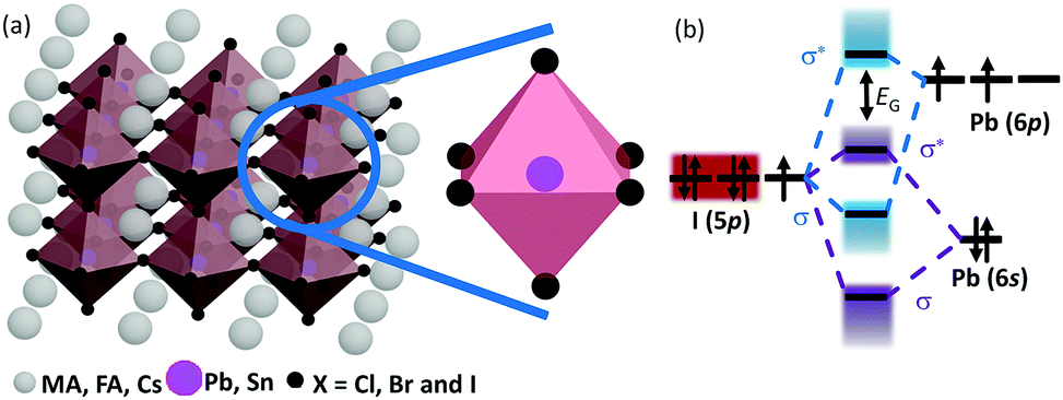
The chemical formula of halide perovskites can be represented as ABX3, where A and B are two different kinds of cations and X is a halide anion (Cl, Br and I). Cation B localizes at the body center of the octahedron composed of six halide anions ([BX6]4−) as illustrated in Scheme 2a. In the cubic-symmetry, the octahedra are linked with each other by sharing the vertex. Cation A can be organic and/or inorganic and is in a 12-fold cuboctahedral coordination (Scheme 2a).17 To predict the generation of a halide perovskite, the tolerance factor , where RA, RB and RX are the ionic radii of the corresponding ions, should be between 0.8 and 1.1.49–51 Cubic perovskites are usually observed at high temperatures. As the temperature decreases, the octahedra begin to tilt, which results in a series of lower symmetry phases, including tetragonal, orthorhombic, monoclinic and rhombohedral. The successive phase transitions can be attributed to the doubly bridging halide ion (B–X–B moiety), which is directly relates to the electronic structures of halide perovskites and thus influenced their properties.52,53 Theoretical calculations54 indicated that a lower degree of octahedral tilting correlates with a greater contribution of the metal p orbital to the CBM, which results in larger spin–orbital splitting of the CBM and thus a reduced band gap. Table 1 summarizes the unit cell parameters of some common halide perovskites and their optoelectronic properties. Usually, halide perovskites in the cubic phase exhibit the smallest band gap and the highest conductivity. In the case of iodide perovskites, the change in the B–I–B angle hinders charge transport through the inorganic framework as the phase transition progresses at lower temperatures.62 For [PbI6]4−, the valence band maximum (VBM) consists of antibonding I(5p)–Pb(6s) interactions, while the conduction band minimum (CBM) is formed from antibonding I(5p)–Pb(6p) orbitals with the predominant character of the Pb(6p) atomic orbital (Scheme 2b).23,77 Therefore, the band gap is directly related to the cation B and the halide composition, which is experimentally proven by the dependence of the band gap on the stoichiometric ratio of the halide composition.78 Under light illumination, mixed-halide perovskites show photoinduced segregation, i.e. the Hoke effect.79 Bischark80 suggested that compositional non-uniformity results in phase segregation. Upon light illumination, the generated carriers induce lattice distortions, which elevate the enthalpy of mixing. This results in two (instead of one) minima of the free energy. Such a model indicates that the existence of compositional non-uniformity prior to illumination will promote the enrichment of iodide due to the reduced band gap of I-rich domains. As a result, the composition uniformity is important for the stability of halide perovskites.
 | ||
| Scheme 2 (a) Schematic representation of the halide perovskite crystal structure. (b) The bonding (σ) and anti-bonding (σ*) orbitals in MAPbI3. | ||
| Formula | Unit cell dimensions | Crystal system | Space group | Transition temperature (K) | Band gap (eV) | Lifetime (bulk, ns) | Trap density (cm−3) | Ref. | |
|---|---|---|---|---|---|---|---|---|---|
| Angle length (°) | Angle bond (°) | ||||||||
| MAPbCl3 | a = b = c = 5.666(2) | α = β = γ = 90 | Cubic |
Pm![[3 with combining macron]](https://www.rsc.org/images/entities/char_0033_0304.gif) m m |
(Cubic, α-phase) | 2.88 | 83 ± 4 | 3.1 × 10¹⁰ | 55–58 |
| 177.2 | 662 ± 44 | ||||||||
| a = 11.1763 (10); | α = β = γ = 90 | Orthorhombic | Pnma | (Tetragonal, β-phase) | |||||
| b = 11.3409 (10); | 171.5 | ||||||||
| c = 11.2804 (10) | (Orthorhombic, γ-phase) | ||||||||
| MAPbBr3 | a = b = c = 5.933(2) | α = β = γ = 90 | Cubic |
Pmm |
(Cubic, α-phase) | 2.31 | 41 ± 2 | (5.8 ± 0.6) × 109 | 55 and 58–61 |
| 236.3 | (Cubic) | 357 ± 11 | |||||||
| (Tetragonal, β-phase) | 2.22 | ||||||||
| 155.1 | (Tetragonal) | ||||||||
| (Tetragonal, γ-phase) | |||||||||
| 148.8 | |||||||||
| (Orthorhombic, δ-phase) | |||||||||
| MAPbI3 | a = b = c = 6.391(1) | α = β = γ = 90 | Cubic |
Pmm |
(Cubic, α-phase) | 1.54 | 22 ± 6 | 3.6 × 10¹⁰ | 22, 55, 58, 61 and 62 |
| a = 8.849 (2); | α = β = γ = 90 | Tetragonal | I4cm | 330.4 | 1032 ± 150 | ||||
| b = 8.849 (2); | (Tetragonal, β-phase) | ||||||||
| c = 12.642 (10) | 161.4 | ||||||||
| (Orthorhombic, γ-phase) | |||||||||
| CsPbCl3 | a = b = c = 5.605 | α = β = γ = 90 | Cubic |
Pmm |
(Cubic) | 2.85 | — | — | 63,64 |
| 320 | |||||||||
| (Tetragonal) | |||||||||
| 315 | |||||||||
| (Orthorhombic) | |||||||||
| CsPbBr3 | a = 8.2440 (6); | α = β = γ = 90 | Orthorhombic | Pnma | (Cubic) | 2.26 | 4.4 ± 0.1 | 3.6 × 10¹² | 62 and 65–69 |
| b = 11.7351 (11); | 404 | 30 ± 3 | |||||||
| c = 8.1982 (8) | (Tetragonal) | ||||||||
| 325 | |||||||||
| (Orthorhombic) | |||||||||
| CsPbI3 | a = 10.4342 (7); | α = β = γ = 90 | Orthorhombic | Pnma | (Cubic, α-phase) | 1.76 | — | — | 62 and 70–72 |
| b = 4.7905 (3); | 634 | (Cubic); | |||||||
| c = 17.7610 (10) | (Orthorhombic, δ-phase) | 2.78 | |||||||
| (Orthorhombic) | |||||||||
| FAPbBr3 | a = b = c = 5.9944 | α = β = γ = 90 | Cubic |
Pmm |
— | 2.27 | 687 ± 23 | 9.6 × 10⁹ | 60, 73 and 74 |
| (Cubic, Pmm); |
2272 ± 43 | ||||||||
| 2.16 | |||||||||
| (Cubic, Im); |
|||||||||
| 2.10 | |||||||||
| (Pmm) |
|||||||||
| FAPbI3 | a = b = c = 6.3573 | α = β = γ = 90 | Cubic |
Pmm |
(α-phase) | 1.51 (α-phase); | 32 | 1.13 × 10¹⁰, 1.5 × 10¹¹ | 62, 73, 75 and 76 |
| a = 8.6603 (14); | α = β = 90; | Hexagonal | P63mc | 423 | 2.14 (δ-phase) | 484 | (α-phase); | ||
| b = 8.6603 (14); | (δ-phase) | 2.6 × 10¹² (δ-phase) | |||||||
| c = 7.9022 (6) | γ = 120 | (Tetragonal, β-phase) | |||||||
| a = 17.7914 (8); | α = β = 90; | Trigonal | P3 | 140 | |||||
| b = 17.7914 (8); | (Trigonal, γ-phase) | ||||||||
| c = 10.9016 (6) | γ = 120 | ||||||||
| a = b = 8.98; | α = β = 90; | Trigonal | P3m1 | ||||||
| c = 11.01 | γ = 120 | ||||||||
Although cation A works as a counterion for charge balance, it can also indirectly influence the octahedral orientation by steric and Coulombic interactions. For instance, as cation A changes from formamidinium over methylammonium to cesium, the B–I–B angle changes from 179.9° over 163.6° to 153.2° along with band gaps of 1.48 eV, 1.51 eV and 1.67 eV in FAPbI3, MAPbI3 and CsPbI3, respectively.51,53 The effect of cation A on the band gap was also observed in tin halide perovskites.81 Moreover, when cation A possesses an asymmetric structure, it may display a permanent dipole moment (e.g. methylammonium, 2.3 D). The dynamic reorientation of cation A within the cuboctahedral halide cage may respond to external perturbations, which leads to profound effects on the dielectric characteristics of the halide perovskite.82,83 The effects of internal motion of cation A on the property of halide perovskites have been discussed in detail by Walsh.84 Moreover, the component A is also helpful to limit the Hoke effect. When MA was substituted by FA or Cs, the stability was improved.79
Halide perovskites are highly defect-tolerant, even though they possess a high intrinsic defect density, which only has little negative effect on μ and τ.23 The high defect-tolerance of halide perovskites can be attributed to the localization of the VBM at the antibonding orbital between the metal Pb atom and the iodide atom (Scheme 2b), because semiconductors with antibonding states at the top of the valence band are likely to be tolerant to defects.85
Due to the high defect-tolerance, even polycrystalline halide perovskites display excellent optoelectronic properties. Nevertheless, elimination of defects in halide perovskites is essential for optoelectronic devices.86 Single crystalline semiconductors usually exhibit better optoelectronic properties than their polycrystalline counterparts due to fewer crystal boundaries and higher compositional homogeneity. For instance, the trap density of single crystalline MAPbI3 is lower by five orders of magnitude than that of polycrystalline materials.40 By virtue of the excellent optoelectronic properties of the single crystalline material, highly crystalline materials have been used as visible light photodetectors,87–89 and X-ray90,91 and γ-photon detectors.92 Consequently, single crystalline materials are still desirable for excellent performance. The temperature-lowering method,40 inverse temperature crystallization,93 anti-solvent vapor-assisted crystallization61 and other methods for preparing bulk single crystals have been developed and summarized.94 As mentioned above, tilting of the [BX6]4− octahedra is sensitive to temperature and affects the optoelectronic properties. The crystallization temperature and stability of the crystallization conditions are key factors for the preparation of homogeneous and highly crystalline halide perovskites. Recently, Snaith et al. have investigated the crystallization mechanism of the inverse temperature crystallization. Addition of protons elevates the concentration of the solute, and weakens the interaction between solute and solvent and thus prompts the crystallization to happen at low temperatures.95
3.2 Effect of grain size on the properties of halide perovskites
For the fabrication of halide perovskite solar cells, a series of approaches have been developed to control the grain size of the perovskite layer with the aim to elevate the solar cell performance. Since the approaches have been well documented,48,96 a few typical examples showcasing a clear relationship between morphology and performance are discussed in the following.The size effect of the halide perovskite on the performance of the mesoporous scaffold solar cell was first reported by the Grätzel and Park group.42,97 MAPbI3 was prepared by using a two-step spin-coating procedure and the cuboid size was controlled by the concentration of MAI. As the MAI concentration was increased from 0.038 M to 0.063 M, the cuboid size of MAPbI3 decreased from ∼720 nm to ∼90 nm (Fig. 1a) along with a decline in the short circuit current (JSC) of the solar cells from 21.68 ± 0.63 to 19.27 ± 0.55 mA cm−2, which was attributed to light scattering by the larger-sized MAPbI3 cuboids (Fig. 1a and b). In the meanwhile, the open-circuit voltage (VOC) and the fill factor (FF) were maximized when a 0.050 M solution was used. Finally, the cell with medium sized cuboids displayed a PCE of 17.01%. This result was attributed to the increased number of grain boundaries, leading to elevated series resistance as the cuboid size decreased. The long carrier lifetimes and long diffusion lengths in the bulk of halide perovskites motivated the simplification of the device structure.98 From a device structure possessing a mesoporous scaffold of a few micrometers in thickness, the device structure was simplified by obviating mesoporous layer. Thus, the perovskite layer is solely deposited on a flat electron transport layer (ETL). Although the device configuration changed from meso to planar, the grain size control of the halide perovskite was also important. Ohkita and coworkers100 fabricated a planar perovskite solar cell using spin-coating from a N,N′-dimethylformamide (DMF) solution followed by chlorobenzene (CB) dripping during spin-coating to induce crystallization. The grain size is proportional to the concentration of the precursor solution, i.e. the size of MAPbI3 is estimated to be ∼100 nm from 25% stock solution, ∼300 nm from 45% stock solution and ∼500 nm from 55% stock solution. And the thickness of the halide perovskite layer is consistent with grain size. All photovoltaic parameters (JSC, VOC, FF and PCE) improved as the grain size increased. A PCE efficiency of 19.4% was obtained for MAPbI3 perovskite solar cells with the largest grain size being ∼500 nm. The investigation showed that the trap density of MAPbI3 decreased as the grain size increased, which resulted in higher VOC. However, the higher VOC of planar perovskite solar cells with larger MAPbI3 grains indicates that other mechanisms such as surface recombination should be taken into consideration for improving VOC as well.
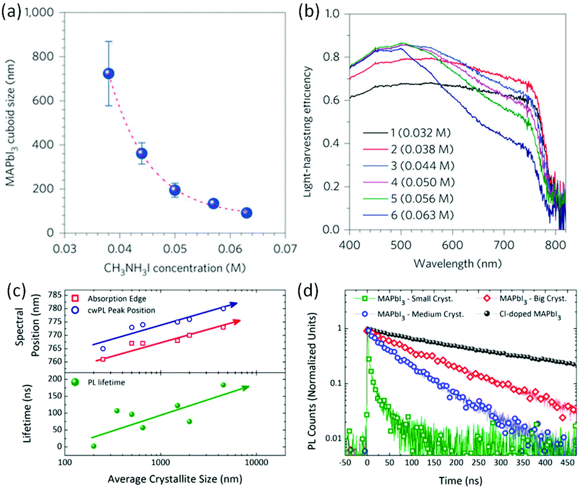 | ||
| Fig. 1 (a) The dependence of the MAI concentration on the MAPbI3 cuboid size. (b) The relationship between the MAPbI3 cuboid size and the light harvesting efficiency; reprinted with permission from ref. 42. Copyright © 2014, Springer Nature. (c and d) Spectral position and lifetimes of the different cuboid sizes. Reprinted with permission from ref. 99. Copyright (2014) American Chemical Society. | ||
It is well known that larger crystals usually show monocrystalline properties and thus are advantageous for electron transport. However, it is highly challenging to control the grain size and grain boundaries for planar perovskite solar cells. Thus, understanding of the thin film formation mechanisms and improvement of process engineering have led to a rapid increase in the power conversion efficiencies of perovskite solar cells. Usually, the low performance of planar devices is attributed to pin-hole formation in the perovskite layer.101,102 In addition, incomplete coverage leads to diminished efficiencies by opening shunting pathways that create current losses and lower light absorption. As a result, one of the main challenges in planar perovskite layers is the deposition of dense halide perovskite layers with full coverage, large grains, and minimized numbers of pinholes to achieve high performances. During the crystallization, the precursor film deposited on the substrate is thermodynamically unstable. Thus, the salts in the precursor can aggregate and further affect the grain size of the halide perovskite.
Annealing temperature is one important factor for controlling the grain size of halide perovskites. Hot casting is useful to control the perovskite morphology and to obtain large and pinhole-free grains. For this, a solution of PbI2 and MACl is heated up to 70 °C and subsequently casted onto a heated substrate. As the substrate temperature increased from room temperature to 190 °C, the grain size of the perovskite dramatically increased ∼1 to 2 mm without pin-holes.103 The obtained perovskites displayed a reduced number of interfacial boundaries along with large grains, leading to suppressed charge trapping and elimination of the hysteresis of the device. Moreover, large grains had a lower number of bulk defects and high mobility, which resulted in a high solar cell efficiency of 17.7%. The Snaith group reported that the film morphology changed from continuous layers with pores to islands with large vacant sites between the grains, as the annealing temperature increased from 90 to 170 °C.104 These morphological changes mainly occur in mixed halide perovskites when PbCl2 is employed as an inorganic source.105 PbCl2 undergoes a different topotactic self-assembly process during the initial annealing stage. The obtained perovskite domains are sharply faceted, which makes it difficult to control the morphology.
This observation also indicated that the precursors of halide perovskites play an important role in the morphology of the obtained film. Firstly, the ratio of the precursor components affects the perovskite morphology. Precursor solutions are made by mixing organic and inorganic sources. The inorganic component PbI2 tends to have a trigonal structure with (001) planes through the van der Waals force, while CH3NH3PbI3 has a tetragonal phase. In the precursor solution, PbI2 and CH3NH3PbI3 form a soft coordination framework as an intermediate phase. The PbI2 phase breaks down and coordinates with DMF, and CH3NH3I is introduced into the phase. In addition, as CH3NH3I dissolves, PbI2 is prone to precipitate. Thus, the organic compound plays a key role in the colloidal precursor solution which determines the obtained perovskite morphology. When excess methylamine hydrochloride (MACl) (MACl![[thin space (1/6-em)]](https://www.rsc.org/images/entities/char_2009.gif) :MAI:PbI2 = 0.95:1.05:1) was added into the precursor solution, the devices showed the best efficiency of 17.04% with well-defined grains and grain boundaries.106,107 Secondly, the precursor source is also crucial for the film morphology. When lead acetate (PbAc2) was used as the non-halide lead source instead of lead chloride or iodide, the obtained perovskite layer was much smoother than that using PbCl2 or PbI2 along with full coverage on the substrate and the absence of pin-holes. The perovskite layer obtained from the PbAc2 route produced CH3NH3Ac as the byproduct, which was easily removed in a short time compared with CH3NH3Cl and CH3NH3I generated from PbCl2 and PbI2. It was also proven that the perovskite layer displayed a much lower activation energy (Ea) of crystallization when PbAc2 was used as the precursor. Thus, this organic lead source facilitates control over the crystal growth, leading to better films and improved performances of solar cells.108
:MAI:PbI2 = 0.95:1.05:1) was added into the precursor solution, the devices showed the best efficiency of 17.04% with well-defined grains and grain boundaries.106,107 Secondly, the precursor source is also crucial for the film morphology. When lead acetate (PbAc2) was used as the non-halide lead source instead of lead chloride or iodide, the obtained perovskite layer was much smoother than that using PbCl2 or PbI2 along with full coverage on the substrate and the absence of pin-holes. The perovskite layer obtained from the PbAc2 route produced CH3NH3Ac as the byproduct, which was easily removed in a short time compared with CH3NH3Cl and CH3NH3I generated from PbCl2 and PbI2. It was also proven that the perovskite layer displayed a much lower activation energy (Ea) of crystallization when PbAc2 was used as the precursor. Thus, this organic lead source facilitates control over the crystal growth, leading to better films and improved performances of solar cells.108
These findings suggest that the properties of perovskites (such as morphology, carrier mobility and grain size) could be changed by controlling the intermediate state during crystallization.109–112 Additives were used to control the intermediate stage of perovskites. For example, sodium ions were added into the precursor solution and micron sized perovskite grains were obtained with the absence of pinholes resulting in an efficiency of 14.2%.113 Hydroiodic acid (HI) was also used to improve the morphology of formamidinium lead iodide (FAPbI3). In addition, 1% of 1,8-diiodooctane (DIO) was added in the precursor solution, which led to an increased efficiency of 11.8% because DIO induces homogeneous nucleation and modulates the growth kinetics.112
The relationship between the grain size and photophysical parameters may explain the effect of morphology on device performance. Petrozza and Kandada96,99 reported on the photophysical parameters of methylammonium trihalide perovskites. For particles ranging from tens of nanometers to a few micrometers, larger MAPbI3 crystallites display smaller band gaps and lower radiative recombination coefficients, resulting in longer lifetimes (Fig. 1c and d), which should be beneficial for achieving high performances. Moreover, larger grains also possess higher absorbance coefficients. The relationship between grain size and optoelectronic properties was also observed in halide perovskite based semiconductor lasers. Xiong and coworkers114 have demonstrated that methylammonium trihalide perovskite platelets with a thickness of tens to hundreds of nanometers form high-quality planar whispering gallery mode cavities, which ensure adequate gain and efficient optical feedback for low-threshold optically pumped lasing. As the edge length of the platelet is increased, the lasing wavelength shifts to lower energy and higher cavity quality factors are obtained, indicating an increase in the net optical gain (Fig. 2).
 | ||
| Fig. 2 (a) Lasing spectra of the triangular CH3NH3PbI3 whispering-gallery-mode cavity (WGM) with different edge lengths. (b) Wavelength of lasing modes (pink stars) and Q-factor (green dots) as a function of the triangular cavity edge length in panel (a). Reprinted with permission from ref. 114. Copyright (2014) American Chemical Society. | ||
As shown in the example mentioned above, the photophysical parameters of halide perovskites clearly depend on the grain size, which significantly affects device performances for light harvesting applications. In principle, optoelectronic properties of halide perovskites are directly related to carrier mobility and radiative lifetimes, which are dependent on the crystal boundaries and crystal defect density. Consequently, the grain size of the halide perovskite in devices, seen as the observable parameter of crystallinity, is an important factor and should be improved to fabricate devices with high performances. However, correlating structural parameters directly to the device performance is difficult, since several factors are influenced upon modulation of the grain size. In this context, nanostructured halide perovskites are advantageous to study structure–property relationships because they can be regarded as single crystalline materials and thus excluding several factors like the influence of grain boundaries.
4. Structural properties of nanoscale halide perovskites
Nanostructured halide perovskites have proven to be disruptive in the field of colloidal semiconductor nanocrystals (NCs) and exhibit blooming prospects for television displays, light-emitting devices, photodetectors and solar cells.115–119 Nanomaterials of halide perovskites can be achieved via various top-down and bottom-up approaches. Most prominently, ligand stabilized halide perovskite nanostructures can be prepared with various aliphatic amines and/or acids which prevent the halide perovskite nanostructures from agglomeration, and restrict the growth. Besides ligand mediated syntheses of halide perovskite nanostructures, impregnation has emerged as an effective route towards highly stable halide perovskite nanostructures with controllable photoluminescence (PL) properties and high quantum yields. Since the charge of individual constituents of a halide perovskite is half of that of the oxidic perovskites such as SrTiO3, halide perovskites typically have much lower crystal lattice energy. This not only leads to lower melting points but also, and more importantly, to lower formation energy of point defects. Consequently, halide perovskites inherently possess a high concentration of crystal defects (as high as several percent120). In most semiconductors, these defects lead to allowed electronic states within the electronic bandgap, which function as charge carrier recombination centers and therefore drastically reduce the efficiency of solar cells or the emission quantum yields in photoluminescence applications. However, as several theoretical studies imply, point defects in halide perovskites do not lead to the formation of intraband states, but rather lead to the formation of electronic states within the valence and conduction band, or to shallow trap states which are close to these bands and therefore only act as weak recombination centers.121 This defect tolerance of halide perovskites implies that, unlike for typical semiconductor nanoparticles for light harvesting applications, neither elaborate synthetic strategies nor surface passivation steps are necessary for the fabrication of, for example, highly luminescent halide perovskite nanostructures, though these elaborate synthetic strategies and/or post-treatment can improve the optical properties.122,1234.1 Surfactant-assisted nanostructured halide perovskites
Colloidal halide perovskite nanoparticles can be synthesized with surfactants that restrict crystal growth in one or more dimensions. Such surfactants are usually ammonium halides with medium to long hydrocarbon chains, such as octylammonium124–126 and oleylammonium halides,47 as well as medium to long chain carboxylic acids. Different from the short methyl ammonium cations that incorporate into the voids between the corner sharing [PbX6]4− octahedra to form the perovskite structure, the long alkyl chain prohibits the incorporation into the bulk. Generally, the polar ammonium end of the capping agent can only be incorporated into the periphery along with the nonpolar alkyl chain dangling outside. As a result, the surfactants limit the growth of the halide perovskite nanoparticles as well as their aggregation. Surfactant-assisted syntheses give access to a surprising variety of 0 dimensional (0D), one dimensional (1D), and two dimensional (2D) halide perovskite nanomaterials. These nanomaterials can be applied in LEDs, solar cells, laser, and field effect transistors by manipulating their dimensionality. In the following sections, the syntheses and properties of surfactant-assisted halide perovskite nanoparticles will be discussed depending on their dimensions.The reprecipitation method is a simple protocol for preparing halide perovskite nanoparticles by mixing the dissolved halide perovskite precursor and the capping agents with an anti-solvent (i.e. a solvent in which the halide perovskite has low solubility). By this, the halide perovskite nanostructures precipitate quickly with adjustable morphologies. The non-templated synthesis of hybrid halide perovskite quantum dots and that of halide perovskite nanostructures in general were pioneered in 2014 by the work of Schmidt et al. (Fig. 3a).124 The facile solution-based process comprises the addition of perovskite precursor solutions in DMF to a solution of octadecylammonium bromide in octadecene (ODE) in the presence of oleic acid at 80 °C. The long alkyl chain ammonium cations act as capping agents to restrict the growth of perovskite particles in all three dimensions. When the ratio of octadecylammonium bromide to MABr is set at 1:1, 3:2 and 7:3, the quantum dots emit light at 529, 526 and 524 nm along with a full width half maximum (FWHM) of 26, 24 and 23 nm, respectively. When octadecylammonium bromide was replaced by octylammonium bromide, the quantum dots (QDs) displayed greater compositional homogeneity, indicating the influence of capping agents on the size of QDs. The prepared quantum dots show quantum yields as high as 20% and are stable in the solid state over months. When the QDs were used as electroluminescent materials, a higher PL intensity compared to that of the bulk material was observed. The optimization of the synthesis protocol was achieved by removing oleic acid and setting the ratio of OABr/MABr/PbBr2 to 2.4/1.6/1. By this, the quantum efficiency of MAPbBr3 QDs was improved to higher than 80%.130
 | ||
| Fig. 3 (a) The TEM images of MAPbBr3 quantum dots, scale bar, 2 nm. Reprinted with permission from ref. 124. Copyright (2014) American Chemical Society. (b) Photographs, photoluminescence spectra and the colors in the CIE diagram of MAPbX3 (X = Cl, Br and I). Reprinted with permission from ref. 131. Copyright (2015) American Chemical Society. | ||
Similar to Schmidt's method, Zhang et al.131 prepared MAPbBr3 QDs displaying an average diameter of 3.3 ± 0.7 nm and emission at 515 nm along with a FWHM of 21 nm by mixing a DMF solution of MAPbBr3 precursors, n-octylamine and oleic acid into toluene. Compared with the bulk material, the QDs displayed ∼30 nm blue shift and two short PL lifetimes resulting from the recombination of initially generated excitons and of surface states involved excitons, respectively. In addition, the MAPbBr3 QDs displayed a larger exciton binding energy (∼375 meV) than that (∼65 meV) of the bulk counterpart, which can be responsible for the generally higher quantum yields of the QDs. Moreover, the results also suggested that the PL emission of QDs took place through exciton recombination than recombination of free electrons and holes due to the enhanced exciton stability, which was also confirmed by the strong exciton–phonon interactions (∼42.2 meV optical phonon energy). Additionally, the synthetic method is also feasible with different halide composition (Cl, Br and I). As a result, the absorption and PL spectra of the highly emissive QDs can be tuned from 407 to 734 nm along with small FWHM (20–50 nm), which demonstrates their great potential applications in display devices (Fig. 3b). By injecting the DMF solution, which contains the precursors and surfactants, into toluene, Rogach's group132 adjusted the size of the MAPbBr3 QDs between 1.8 and 3.6 nm by varying the injecting temperature between 0 and 60 °C. Lower synthesis temperatures resulted in smaller diameters of the QDs. As a result, the emission could be tuned between 475 and 520 nm with quantum yields as high as 93% without changing the composition of the QDs.
Time-resolved PL measurements showed one uncommon phenomenon, which is that the lifetime of the smaller QDs was longer than that of the larger QDs. This unusual observation was attributed to the overlap integral between electron and hole wavefunction, and the higher optical permittivity of the small particles. The results from Rogach's group also demonstrated that the PL wavelength can be tuned by the size of the quantum dots. Consistent with this, Hassan et al.47 demonstrated the relationship between the structure and the optical properties of the MAPbI3 QDs (Fig. 4a and b). Firstly, PbI2 QDs were first prepared by injecting the iodide–amine complex into a solution of lead–oleate complex (2 mM) in ODE. PbI2 QDs of 3.8 ± 0.4, 5.3 ± 0.5, and 9.7 ± 0.3 nm diameter were prepared at growth interval times of 5, 15 and 30 min, respectively. Later, the differently sized PbI2 QDs were exposed to MAI and/or the long-chain ammonium iodide at 50 °C for 30 s to be converted into differently sized MAPbI3 QDs. Moreover, by controlling the ratio of MAI to oleylammonium iodide, the layer number (n) of the MAPbI3 QDs can be adjusted to 1, 2 and 3. When n = 3, the first exciton is 585, 592 and 599 nm for sizes of 3.5, 5.5 and 10 nm, respectively. When the diameter was 5.5 nm, the absorption peak localized at 505, 565 and 593–600 nm for n = 1, 2 and 3, respectively. Moreover, as the length of the hydrocarbon chain of the surfactant increased, the absorption peak shifted to longer wavelength.
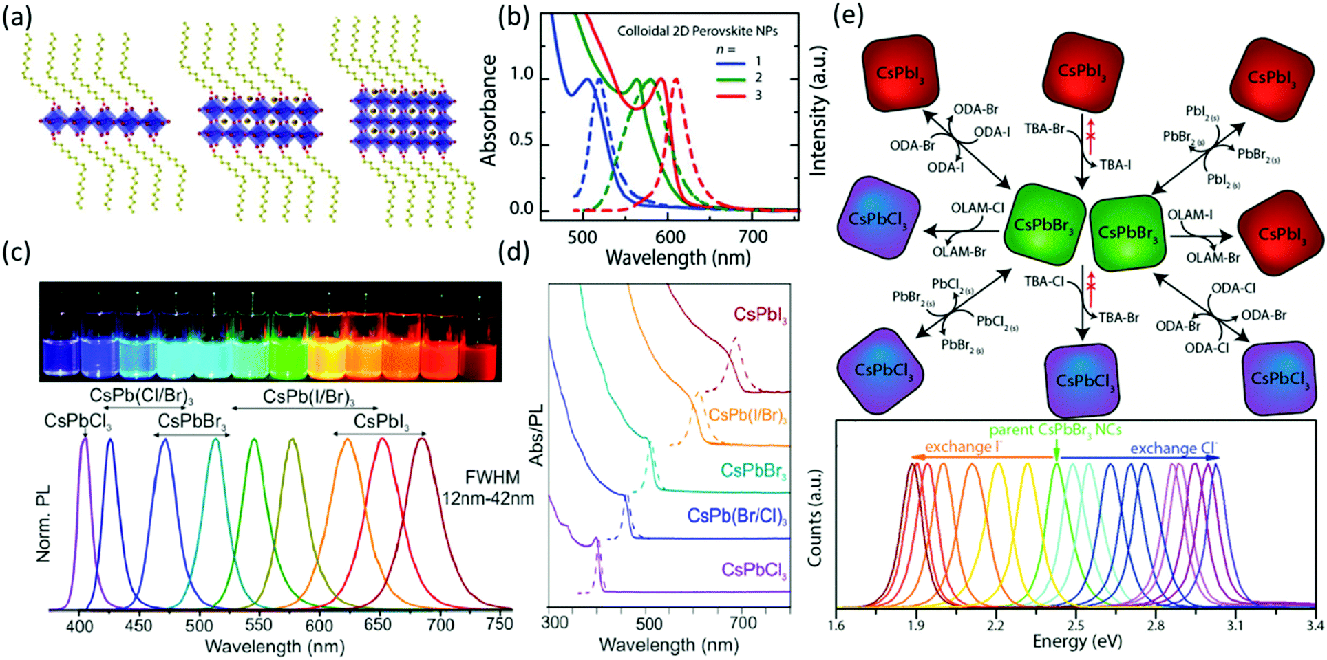 | ||
| Fig. 4 Schematic representation of MAPbI3 quantum dots (a) and their corresponding PL spectra (b) with different layers of halide perovskites; reprinted with permission from ref. 47. Copyright © 2015 Wiley-VCH Verlag GmbH & Co. KGaA, Weinheim. Photographs and PL spectra (c) and the absorbance spectra (d) of CsPbX3 (X = Cl, Br and I) quantum dots. Reprinted with permission from ref. 78. Copyright (2015) American Chemical Society. (e) The synthetic route and the PL spectra of halide exchange among CsPbX3 (X = Cl, Br and I) quantum dots. Reprinted with permission from ref. 134. Copyright (2015) American Chemical Society. | ||
Due to the better stability of all inorganic halide perovskites, this class of halide perovskites showed more promising applicability for light emitting devices than organic–inorganic halide perovskites. In 2015, Protesescu et al.78 demonstrated the synthesis of all-inorganic CsPbX3 halide perovskites by hot injection (Fig. 4c and d). In the synthesis, CsBr (in analogy to MABr in MAPbBr3) cannot be used as a precursor due to its low solubility. To overcome this issue, the authors synthesized Cs-oleate from CsCO3, which has a higher solubility and acts as the Cs-precursor. Moreover, by varying the halide component, highly luminescent perovskite quantum dots with tunable emission spectra and quantum yields as high as 90% can be fabricated with edge lengths between 4 and 15 nm. As in the case of methylammonium halide perovskites, the bandgap of CsPbX3 increases as the edge length decreases. More interestingly, Kuno et al.133 reported that the Stokes shift of CsPbBr3 nanocrystals decreases as the edge length increases. Akkerman et al.134 extended the work in the field of all inorganic halide perovskites by varying the halide component of the perovskite using an anion exchange reaction to fabricate caesium lead halide perovskites with different halide components from CsPbBr3. In their works, the authors described the halide exchange reaction as a dynamic process that takes place in solution (Fig. 4e). Therefore, also mixing perovskite quantum dots with different halide compositions leads to homogenization of their composition and of their emission properties. Other groups reported similar halide exchanges on CsPbBr3 quantum dots135 and thin films.136 By modifying the reprecipitation method131 of the inorganic halide perovskite QDs, ∼11 nm CsPbX3 (X = Cl, Br and I) QDs were prepared137 with PL emission between 400 and 650 nm. Compared with the QDs prepared from hot injection, the QDs prepared from the reprecipitation method displayed similar quantum yields and FWHMs of the PL ranged from 12 to 39 nm. The CsPbBr3 QDs demonstrated an exciton binding energy of ∼40 meV and an optical phonon energy of 4.6 meV, both of which are one order of magnitude lower than that of MAPbBr3 QDs (Table 2). The radiative and non-radiative lifetimes of CsPbBr3 QDs are on the time scale of nanoseconds, and the shorter lifetimes of radiative recombination as compared to the non-radiative recombination in CsPbBr3 QDs should be responsible for their high quantum yield. It should be pointed out that nanostructured halide perovskites are sensitive to the environment and the sample quality. The photophysical parameters of some common nanostructured halide perovskites are summarized in Table 2.
| Formula | Morphology | Size (nm) | Emission (nm) | FWHM (nm) | Quantum yield (%) | Lifetime | Exciton bind energy (meV) | Ref. |
|---|---|---|---|---|---|---|---|---|
| a n represents the number of layers in the quantum dots. b The data were obtained from the MAPbI3 QDs with diameter = 5.5 nm and n = 3; for NPLs, L represents the lateral size and t represents the thickness. | ||||||||
| MAPbBr3 | Nanocube | 3.3 ± 0.7 | 515 | 21 | 50–70 | 6.6 ns (63.6%) | 375 (5–300 K) | 131 |
| 18.0 ns (36.4%) | 42 (300–400 K) | |||||||
| 1.8 | 475 | 28–36 | 74 | 36.8 ns (τr) | — | 132 | ||
| 104.8 ns (τnr) | ||||||||
| 2.8 | 500 | 89 | 16.3 ns (τr) | |||||
| 128.2 ns (τnr) | ||||||||
| 3.6 | 521 | 93 | 19.6 ns (τr) | |||||
| 252.6 ns (τnr) | ||||||||
| MAPbI3 | 3.5 | 585 | 31b | 20b | 250 fs (22%)b | — | 47 | |
| 5.5 | 505 (n = 1)a | 69 ps (12%) | ||||||
| 565 (n = 2)a | 5.63 ns (67%) | |||||||
| 593–600 (n = 3)a | ||||||||
| 10 | 599 | |||||||
| CsPbCl3 | Nanocube | 8.0 ± 1.4 | 389 | 14 (0.12 eV) | 1 | — | 75 | 134 |
| — | 405 | 12 | 10 | |||||
| CsPbBr3 | Nanocube | 11.5 | 513 | 20 | 95 | 8.9 ns (cubic phase) | 40 | 137 |
| 10.5 | 513 | 20 | 95 | 8.2 ns (monoclinic) | ||||
| 8.4 ± 1.0 | 510 | 26 (0.1 eV) | 78 | — | ||||
| CsPbI3 | Nanocube | 9.1 ± 1.3 | 663 | 38 (0.11 eV) | 36 | — | 20 | 78, 134 |
| CsPbBr3 | NPL (t = 3.4 nm) | L = 7.3 | 478–488 | — | 50–70 | 8.2 ps | 120 | 187 |
| L = 14.8 | ||||||||
| L = 20.2 | ||||||||
| CsPbBr3 | Nanosphere | 4.5 ± 0.9 | 457–515 | — | 81 | 5.9–19.9 ns | — | 188 |
| Nanocube | 9 ± 1 | 514 | — | 5.1 ns (57.89%) | ||||
| 18.7 ns (29.95%) | ||||||||
| 129 ns (12.16%) | ||||||||
| NPL | 100(L) × 5.2(t) | 510 | — | 3.02 ns (11.51%) | ||||
| 140 ns (24.79%) | ||||||||
| 1440 ns (63.7%) | ||||||||
| Nanorods | 200(L) × 10(D) | 515 | — | 264 ps (44.02%) | ||||
| 4.20 ns (24.90%) | ||||||||
| 66.1 ns (31.08%) | ||||||||
| FAPbCl3 | NPL | 22 ± 3 | 416–738 | 20–44 | <1 | 15 | — | 186 |
| FAPbBr3 | NPL | 21.5 ± 4 | 84 | 20 | 24 | |||
| FAPbI3 | Nanocube | 14.4 ± 3.4 | 55 | 116 | 8–10 | |||
Due to the high quantum yield, research on halide perovskite quantum dots mostly focuses on their application as luminophores e.g. in displays.131,138–140 It is desirable that halide perovskite quantum dots can also be assembled as thin films to construct complex layered structures in order to fabricate optoelectronic devices such as LEDs128,141–143 and solar cells.144–146 Moreover, the low stability towards air and moisture is still the key concern. The high surface area of 0D nanoparticles makes them even more prone to degradation. One strategy to overcome this problem is to embed the perovskite QDs in polymers. Encapsulating MAPbBr3 QDs with a silica precursor138,147,148 led to improved stability in moist air without sacrificing the PL quantum yield. Encapsulation not only improves the thermal- and photo-stability of the halide perovskite QDs but also avoids ion exchange between mixtures of halide perovskite QDs with different compositions.139
Beyond this, the higher stability of the all-inorganic halide perovskites makes them interesting materials for photochemical and photocatalytic applications. For example photocatalytic CO2 reduction was reported for CsPbBr3 QDs and CsPbBr3 QDs supported on graphene oxide.33,35 Furthermore, Chen et al. recently reported the photocatalytic formation of poly(3,4-ethylenedioxythiophene) (PEDOT) from EDOT trimers by CsPbI3 QDs. The cubic crystal structure of CsPbI3 quantum dots can be preserved when benzoquinone is added to the reaction suspension as an electron acceptor. The photocatalytic polymerization opens a new route to prepare CsPbI3/PEDOT composites while preserving stability for novel optoelectronic materials and devices.34
 | ||
| Fig. 5 (a) Schematic representation of MAPbX3 nanorod formation; (b) photographs and TEM images of MAPbBrxI3−x nanorods; reprinted with permission from ref. 153. Copyright (2016) American Chemical Society. (c) The effect of hydrogen halide on the morphology of MAPbX3 nanofibers; (d) the UV-vis (solid line) and photoluminescence spectra (dotted line) and photographs of MAPbX3 (X = Cl, Br and I). Reprinted with permission from ref. 154. Copyright (2017) American Chemical Society. | ||
Interestingly, both the band gap and the length of CsPbBr3 NWs can be controlled by adding different amounts of hydrohalic acids (HX, X = Cl, Br and I). The band gap change was attributed to halide exchange. In the meantime, the length control was ascribed to the inhibition role of the ammonium, which was generated from the protonation of oleylamine in the presence of hydrohalic acids (Fig. 5c and d).
One more crucial factor that determines the morphology of halide perovskite nanomaterials is the reaction time. The preparation of 0D halide perovskite quantum dots proceeds via the rapid quenching of the reaction mixture by reducing the temperature shortly after mixing both precursor solutions. Typical timescales between mixing of the precursor solutions and quenching are in the range of a few seconds. However, by increasing the timeframe to 10 minutes and more, NWs readily form.152 Moreover, the band gaps of the NWs can be adjusted by halide exchange and the thickness can be tailored by reprecipitation from the supernatant.155 Chen et al.151 found that the morphology of the nanomaterial also relates to the state of the precursors before reaction. The authors prepared CsPbX3 (X = Cl, Br and I) nanomaterials via a solvothermal method. When the precursors were heated to high temperatures with pre-dissolution, NWs were obtained. When the precursors were only simply mixed, nanocubes were obtained.
Halide perovskite nanowires can be prepared via solution phase as well as vapor phase procedures.156–158 Xing et al.156 prepared free-standing and single crystalline methyl ammonium lead halide nanowires possessing rectangular cross sections and long charge carrier diffusion lengths via a vapour phase process. The emissions of the nanowires in lasing application can be precisely tuned with different halide compositions. Park, Song and coworkers157 utilized PbX2 and CsX (X = Cl, Br and I) as precursors to prepare NWs on a Si substrate by two source gas deposition (Fig. 6a). The obtained NWs showed laser emissions at 420–430 nm for CsPbCl3, 530 nm for CsPbBr3 and 720–730 nm for CsPbI3. The threshold of CsPbBr3 NWs (3 μJ cm−2) is lower than those of chloride (7 μJ cm−2) and iodide analogues (6 μJ cm−2), indicating the better crystal quality of CsPbBr3. This explanation was also supported by the longer charge carrier lifetime of CsPbBr3 (7.2 ns) than the chloride (1.1 ns) and iodide analogues (3.7 ns). Following the same protocol, Jin, Shen and coworkers158 grew the NWs on the phlogopite mica. Different from the Si substrate, the CsPbX3 (X = Cl, Br and I) NWs grew along the mica surface possibly due to the intercalation of Cs+ into the K+ vacancies of the mica and the electrostatic interaction between K+ and Br−. As the reaction proceeded, the NWs gradually grew into films. More interestingly, the NWs displayed a waveguide phenomenon across the intersection of the different NWs (Fig. 6b).
 | ||
| Fig. 6 (a) SEM micrographs and amplified spontaneous emission spectra of CsPbX3 nanowires. Reprinted with permission from ref. 157. Copyright (2016) American Chemical Society. (b) Waveguide effect of CsPbBr3 NWs on a mica surface. Reprinted with permission from ref. 158. Copyright (2017) American Chemical Society. | ||
Lasing is the most prominent application of halide perovskite nanowires and its threshold, mode spacing, and mode positions vary between individual nanowires due to the differences in their morphology (length, shape of end facets and crystalline quality).41,157 Individual NWs form a Fabry–Pérot cavity to achieve the optical feedback necessary for lasing emission. Thus, precise control over the emission properties is a major prerequisite for optoelectronic applications. Relevant parameters of halide perovskite lasers are summarized in Table 3. Zhu et al.41 reported exceptionally low lasing thresholds from solution processed MAPbI3 nanowires of as low as 220 nJ cm−2. Zhu et al. also employed a two-step process with Pb(AcO)2 and MA halides without utilizing capping agents. By tuning the halide composition of the material, lasing was observed at 500 nm and 780 nm, covering wide parts of the visible light spectrum. However, so far all reports about halide perovskite nanowire lasers (and all other halide perovskite structures) exclusively demonstrate optical pumped lasing and no electrically pumped lasing, which would bring halide perovskite nanowire lasers closer to applications.
| Formula | Morphology | Crystallinity | Emission (nm) | FWHM (nm) | Threshold | Q-factor | Ref. |
|---|---|---|---|---|---|---|---|
| Λ is the interval of the periodic line and L is the edge length of the microplate. | |||||||
| MAPbBr3 | Microdisk | Single crystal | 557.5 | 1.1 | 3.6 μJ cm−2 | ∼430 | 196 |
| MAPbBr3 | Microdisk | Single crystal | 553 | 1.7 | 3.5 μJ cm−2 | ∼1090 | 248 |
| 557 | 1.2 | ||||||
| MAPbBr3 | Nanowires | Single crystal | 550 | 0.23 | 300 nJ cm−2 | ∼2400 | 41 |
| MAPbI3 | Nanowires | Single crystal | 787 | 0.22 | 220 nJ cm−2 | ∼3600 | |
| MAPbI3 | Nanowires | Single crystal | 777 | 2 | 11 μJ cm−2 | ∼405 | 156 |
| MAPbBr3 | Inverse opal | Polycrystalline | 545.54 | 0.15 | 1.6 mJ cm−2 | ∼3600 | 233 |
| MAPbI3 | 2D photonic crystal | Polycrystalline | 787.6 | 0.13 | 3.8 μJ cm−2 | ∼6000 | 237 |
| MAPbI3 | Sphere | Polycrystalline | 784.8 (1.58 eV) | 50 ± 4 meV | 65 ± 8 μJ cm−2 | ∼1000 | 240 |
| MAPbI3 | Periodic line (Λ = 403 ± 1) | Polycrystalline | 777.6 | 1.1 | 91 ± 2 μJ cm−2 (λp = 355 nm) | ∼700 | 242 |
| 40 ± 5 μJ cm−2 (λp = 532 nm) | |||||||
| MAPbI3 | Periodic line | Polycrystalline | 760 | 2.2 | 0.32 μJ cm−2 (Λ = 400) | ∼400 | 241 |
| 2.1 | 0.54 μJ cm−2 (Λ = 410) | ||||||
| 1.4 | 2.11 μJ cm−2 (Λ = 420) | ||||||
| MAPbI3 | Periodic line | Polycrystalline | 786.5 (Λ = 370 nm) | 0.2 | 120 ± 24 kW cm−2 | ∼3900 | 243 |
| 794 (Λ = 380 nm) | |||||||
| MAPbI3 | 2D photonic crystal | Polycrystalline | 788.1 | 0.24 | 141.3 ± 3.2 μJ cm−2 (Λ = 430 nm) | ∼3200 | 244 |
| 79.7 ± 4.5 μJ cm−2 (Λ = 440 nm) | |||||||
| 68.5 ± 3.0 μJ cm−2 (Λ = 450 nm) | |||||||
| 82.6 ± 4.4 μJ cm−2 (Λ = 460 nm) | |||||||
| MAPbI3 | Microplate | Single crystal | 782 | 0.64 | 12.8 μJ cm−2 (L = 8.3 μm) | ∼1200 | 247 |
| 785 | 10.8 μJ cm−2 (L = 13.1 μm) | ||||||
| 786 | 10.0 μJ cm−2 (L = 16.8 μm) | ||||||
| 792 | 9.0 μJ cm−2 (L = 19.6 μm) | ||||||
| MAPbI3 | Nanoplatelet | Single crystal | 788 (L = 47 μm) | 0.9–1.2 | 37–128 μJ cm−2 | ∼1300 | 114 |
| 786 (L = 38 μm) | ∼950 | ||||||
| 782 (L = 32 μm) | ∼800 | ||||||
| 780 (L = 28 μm) | ∼650 | ||||||
| CsPbCl3 | Nanoplatelet | Single crystal | 427 (2.9 eV) | 4 meV | 12 μJ cm−2 | ∼300 | 197 |
| CsPbCl3 | Nanowires | Single crystal | 420–430 | 0.3 | 7 μJ cm−2 | ∼1400 | 157 |
| CsPbBr3 | Nanowires | Single crystal | 530 | 0.4 | 3 μJ cm−2 | ∼1300 | |
| CsPbI3 | Nanowires | Single crystal | 720–730 | 0.6 | 6 μJ cm−2 | ∼1200 | |
| CsPbBr3 | Nanoplatelet | Single crystal | 530 | 0.15 | 1.5 μJ cm−2 | ∼3500 | 192 |
| CsPbCl3 | Microdisk | Single crystal | 427 | ∼0.8 | 3–12 μJ cm−2 | ∼530 | 249 |
| CsPbCl2Br1 | 460 | ∼2700 | |||||
| CsPbCl1Br2 | 495 | ∼4100 | |||||
| CsPbBr3 | 540 | ∼1600 | |||||
| FAPbI3 | Nanowires | Single crystal | 824 | 0.53 | 6.2 μJ cm−2 | ∼1500 | 250 |
| (MA,FA)Pb(Br,I)3 | Nanowires | Single crystal | 782 | 0.55 | 2.6 μJ cm−2 | ∼1450 | |
In addition to lasing, hybrid and all-inorganic halide perovskite nanowires are also applied in solar cells.159–162 Park and co-workers demonstrated that nanowire perovskite solar cells possess faster carrier separation and higher lateral conductivity compared to the 3D counterpart as a result of the reduced dimensionality. They reported a power conversion efficiency of 14.7%, which was later increased by Wang et al. to 17.6% by employing a solvent etching treatment with mixtures of polar and nonpolar solvents to tune the roughness of the nanowire film.160 As observed in the 1D nanostructures,158 a waveguide may improve the extraction of light from the active layer and thus enhance the external quantum efficiencies for light emitting diodes.163
Nanowires are also applied as photodetectors and phototransistors due to their high responsivity,158,161,164–168 mechanical flexibility,169 stability,170 pixelated detection,171 and large scale manufacturability.172 Due to the excellent optoelectronic properties, polycrystalline materials displayed good performances. Zhuo et al. reported porous NWs obtained via the conversion of Pb containing NWs into halide perovskites via a MABr and HBr containing solution.165 As a result of the porous structure, the NWs possess superior optoelectronic properties such as high sensitivity, short photo-response, and decay times which make them well-suited as visible light photodetectors.
Nanoplatelet (NPL) is a typical morphology of 2D nanomaterials. The preparation of halide perovskite NPLs can, like the preparation of 1D nanowires, proceed via different solution based approaches or via vapor phase synthesis methods. However, solution based processes are by far more often employed due to the relative simplicity and promptness of these methods.126,177–182 Dou et al.177 prepared atomically thin 2D MAPbX3 NPLs on Si/SiO2 substrates by controlling their crystallization in a DMF–CB co-solvent (Fig. 7).
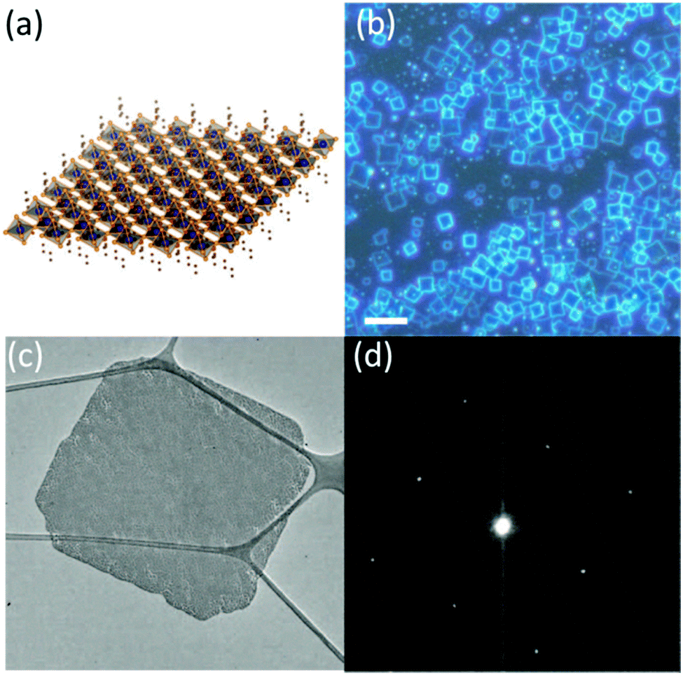 | ||
| Fig. 7 Schematic representation (a), optical images (b), TEM images (c) and the selected area electron diffraction of the MAPbX3 nanosheet (d). Reprinted with permission from ref. 177. Copyright © 2015, American Association for the Advancement of Science. | ||
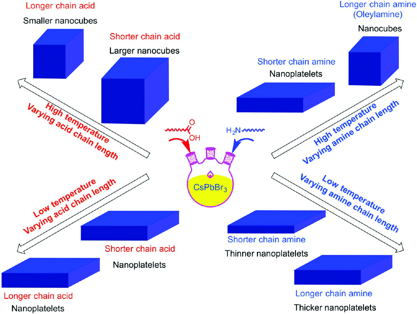
By virtue of the reprecipitation method, Weidman et al. fabricated NPLs in 2016. On dropping a DMF solution containing the perovskite precursors, octylammonium and butylammonium into toluene, halide perovskite NPLs readily form at room temperature within seconds (Fig. 8).178 By tuning the precursor ratio, single and bilayer NPLs were synthesized with excellent control over the thickness. Following this method, thicker NPLs can also be fabricated but with a lesser extent of thickness control. Tuning each of the perovskite components allows precise control over the absorption and emission wavelengths between 2.2 eV (564 nm) and 3.7 eV (335 nm).178 CsPbX3 NPLs with three to five monolayers were fabricated with excellent thickness control via a colloidal synthesis approach.179 All these approaches offer excellent control over the thickness up to a few atomic layers but are limited to the preparation of thin structures. By employing the same method, the Banerjee group also tuned the thickness of MAPbBr3 NPLs between one and six layers by adjusting the concentration and hydrocarbon chain length of the ammonium cation (capping ligand) between 4 and 18 carbons.180 As the carbon number increased, lower diffusion coefficients, higher steric footprint and greater aggregation enthalpy of the ligand molecules resulted in the generation of thinner NPLs along with the photoluminescence emission shifting to short wavelength.180 The morphologies of the nanostructured halide perovskites can be tailored between 0D and 2D structures by controlling the composition of hydrocarbon ammoniums and acids (Fig. 9).183
 | ||
| Fig. 8 Schematic representation (a), absorbance (dotted line) and photoluminescence (solid line) spectra (b) and TEM images (c) of L2[ABX3]n−1BX4 (X = Cl, Br, and I; B = Pb and Sn) nanoplatelets. Reprinted with permission from ref. 178. Copyright (2016) American Chemical Society. | ||
 | ||
| Fig. 9 Schematic representation of the ligand effect on the morphology of the nano CsPbBr3. Reprinted with permission from ref. 183. Copyright (2016) American Chemical Society. | ||
Since it is sufficient to reduce solely one dimension of a particle below the exciton Bohr radius, quantum confinement effects can be observed in 2D NPLs. Thereby, the emission spectrum is independent of the expanse of the NPLs in the two dimensions that are not on the nanoscale. Consequently, halide perovskite NPLs show markedly narrow photoluminescence spectra.175,182,184 Furthermore, the halide perovskite NPLs can be stacked to form oriented assemblies with intense and tunable photoluminescence.185 The absorption spectra and PL emission displayed a blue shift as the thickness of the NPLs decreased, and the quantum yields of the NPLs decreased from 84.4 ± 1.8% over 44.7 ± 2.6% to 10 ± 0.5% as the thickness of NPLs changed from 5 over 4 to 3 unit cells. A similar phenomenon was also observed for FAPbBr3 NPLs.186 As the thickness increased from 1.4 ± 0.1 via 2 ± 0.1 to 2.6 ± 0.2 nm, the emission of NPLs shifted from 438, to 486 and finally to 533 nm along with the quantum yield increasing from 21% to 84%. Li et al.187 studied the exciton behavior of 2D NPLs of CsPbBr3 in terms of oscillator strength and exciton binding energy. These two features are of great importance as they govern the absorption and emission cross sections and the charge carrier transport mechanism. Both of them are fundamental for application in optoelectronic devices. In their study, the authors found oscillator strengths (1.18 × 10⁴) that are much higher than those of colloidal II–VI NPLs and quantum wells, while the exciton binding energies (120 meV) are comparable to those of colloidal II–VI NPLs and quantum wells. Both these properties make halide perovskite NPLs very promising for various optoelectronic applications. The higher exciton binding energy compared to the bulk counterpart is responsible for the shorter lifetime as the thickness decreased. In the meanwhile, the lower quantum yield of thinner NPLs should be attributed to enhanced non-radiative recombination.
By utilizing different acids and amines, Sun et al.188 prepared a series of CsPbX3 nanomaterials with different shapes. When dodecylamine and oleic acid were used, CsPbBr3 crystallized into nanocubes. When dodecylamine was replaced by octylamine, nanoplatelets were obtained. When oleic acid was replaced by acetic acid, CsPbBr3 crystallized into nanorods. When both the acid and amine with long hydrocarbon chains were replaced with hexanoic acid and octylamine, CsPbBr3 crystallized into nanospheres. The emission maxima of the nanospheres localized at 457, 465, 474, 510 and 515 nm by controlling the synthetic temperature at −20, 0, 20, 40 and 60 °C, respectively. As the emission shifted to longer wavelengths, the decay lifetimes were 5.91, 8.59, 10.8, 12.7 and 19.9 ns, respectively. For other nanomaterials, the nanocubes gave lifetimes of 5.18 ns (57.89%), 18.7 ns (29.95%), and 129 ns (12.16%); the nanorods gave lifetimes of 0.264 ns (44.02%), 4.20 ns (24.90%), and 66.1 ns (31.08%); and the nanoplatelets gave lifetimes of 3.02 ns (11.51%), 140 ns (24.79%), and 1440 ns (63.70%). In the case of nanocubes, the long lifetime (129 ns) was attributed to trap states. As for the 2D nanorods, the lifetime of the major component was 0.264 ns which was much shorter than those of the other two components (4.20 and 66.1 ns). In the meanwhile, the nanoplatelets displayed a lifetime of 3.02 ns (11.51%), which was much shorter than those of the other two components, which displayed strong 1D quantum confinement. Due to their relatively large overall size, NPLs can readily be incorporated into optoelectronic devices and allow the fabrication of sophisticated layered structures that are required for applications such as solar cells,189 field-effect transistors175 and LEDs.190 Furthermore, 2D NPLs are single crystalline and exhibit diverse symmetrical shapes making them suitable also for laser emission from whispering gallery modes.
Another solution based approach is the exfoliation of halide perovskite nanoplatelets from bulk perovskite in the presence of excess capping agents.181 This method offers control over the NPL thickness via variation of the dilution and the concentration of the capping ligand. Besides the capping agent, temperature is another important parameter to control the thickness of the NPLs.191 In the presence of pyridine, two-, four- and six-layered NPLs were obtained when the DMF precursor solution was dispersed into the OA and OAm solution in toluene at 0, 25 and 60 °C, respectively. Besides the solution processing method, thicker NPLs with a thickness in the order of tens to hundreds of nanometers can be fabricated by CVD methods192–194 and by PDMS stamping.195
As mentioned earlier, 2D NPLs are well-suited for use in optoelectronic devices. Especially, whispering gallery mode lasing from halide perovskite NPLs is widely reported by many groups.192,196,197 The reported nanolasers possess low excitation thresholds as low as 2 μJ cm−2 under femtosecond pulsed laser irradiation192 and can readily be fabricated on substrates relevant for optoelectronic devices such as Si, Au, indium tin oxide, and others, which is difficult to achieve for 1D nanowires.193
The large lateral dimensions of halide perovskite NPLs allow their easy integration on patterned substrates to fabricate photodetectors. In addition, the single crystalline nature and the high absorbance of the nanoplatelets result in photodetectors with high responsivity and short response times that are better than or comparable to state-of-the-art photodetectors based on halide perovskites.198 More complicated layered structures as light emitting diodes and solar cells can also be fabricated from halide perovskite NPLs and show promising results in terms of wavelength tunability and external quantum efficiency.190,193,199 When phenylethylammonium iodide is used as the ligand, 3D MAPbI3 can be converted into 2D MAPbI3 by tailoring the thickness of MAPbI3. The thinner perovskite material displays higher stability189 and higher quantum yield.200
Very recently, Kagan and Straus et al. have revealed the structure–property relationship of the 2D halide perovskite materials. The reader can refer to their review for further details.201 Because the binding of the capping agent to the nanostructured halide perovskites is highly dynamic,202 their morphologies are susceptible to the ligand in the solution. Balakrishnan et al.203 reported that dodecyl dimethylammonium bromide (DDAB) can induce the transformation of CsPbBr3 nanocrystals into crystalline 2D CsPb2Br5 nanosheets. DDAB promoted the formation of PbBr3−, which further reorganized to form stable [Pb2Br5]−. Concurrently, the morphology changed from nanocubes into 2D nanosheets. As a result, the capping agents play an important role in stabilizing the morphology and crystal phase of halide perovskites. When the halide perovskite single crystal was exposed to ambient air, hydration-induced transformation occurred along with the change of optical properties, charge carrier mobility and the performance of the devices.123 Surface passivation can modulate the surface trap and thus the recombination velocities. For nanostructured halide perovskites, the capping agent also passivated the surface to improve the quantum yield.122 However, the capping agents may also retard or even hinder carrier diffusion across the capping agent layer, and thus deteriorate the optoelectronic property of the materials. For example, the electron transfer from CsPbBr3 to rhodamine only proceeded when rhodamine penetrated into the capping agent layer and the distance was close enough.204
4.2 Confinement of nanoscale halide perovskites in porous structures
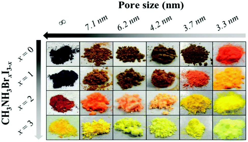
Halide perovskites can be embedded into the pores of various matrices comprising ordered mesoporous silica, silicon, titania, alumina, and organic polymers. The intriguing advantage of halide perovskite nanocrystals over other highly luminescent semiconductors is their good defect tolerance not only towards point defects205,206 but more importantly towards surface dangling bonds.207 In this context, defect tolerance means that defects do not form energetic states within the bandgap, which opens up non-radiative decay pathways, but rather within the conduction or valance bands.208,209 In contrast, most other strongly luminescent quantum dots such as CdSe, InAs, and InP necessitate encapsulation with wider bandgap semiconductors in order to avoid trapping of charge carriers at surface defects within the bandgap, which would strongly attenuate the photoluminescence quantum yield.207 Halide perovskite nanostructures prepared by impregnating into the scaffolds are known from the pioneering work on halide perovskite solar cells in 2011 by Im et al.210 Halide perovskite nanostructures prepared by impregnating into the scaffolds are most often reported for their altered static and dynamic photoluminescence properties, but are also applied in halide perovskite solar cells and for electroluminescence applications.Modified photoluminescence properties of the halide perovskite nanoparticles on the support were firstly demonstrated in 2012 by Kojima et al. As a result of the reduced dimensions of the halide perovskite particles, they observed vastly increased photoluminescence from MAPbBr3 nanoparticles by crystallizing the precursors in a porous alumina support (Fig. 10).211 Later, in 2015 it was also shown that the nanoparticles on alumina support possess reduced photoluminescence decay times.212 Further studies on the optical and optoelectronic properties were mainly focused on silica-supported nanoparticles, since silica supports are available with well-controllable monomodal pore size distributions of different pore sizes and pore morphologies. Accordingly, a broad variety of different supports with diverse textural properties are readily available. Yamauchi et al. prepared a series of MAPbBrxI3−x (x = 0, 1, 2, 3) perovskite nanoparticles in SBA-15, an ordered mesoporous silica support with cylindrical pores, with pore diameters ranging from 3.3 to 7.1 nm (Fig. 11).213
 | ||
| Fig. 10 MAPbBr3 nanoparticles on the support of alumina oxide scaffold by spin-coating. (a) Colorless precursor solution was uniformly dropped onto a mesoporous thin Al2O3 film. (b and c) Quick crystallization of MAPbBr3 during spin coating. Reprinted with permission from ref. 211. Copyright (CY-RT 17-249) Chemical Society of Japan. | ||
 | ||
| Fig. 11 Halide perovskite nanoparticles in the silica support with different pore sizes. Reprinted with permission from ref. 213. Copyright (2016) American Chemical Society. | ||
The perovskite nanoparticles readily form inside the cylindrical pores by a simple impregnation procedure. Thereby the diameter of the 0D and 1D nanomaterials is governed by the pore diameter of the silica support. At particle dimensions below their Bohr radius, quantum confinement results in widened band gaps as a result of the transition from continuous energy bands to discrete energy levels. Consequently, the emission properties of halide perovskites can be precisely tuned by confining halide perovskite nanoparticles in defined silica pores. Together with the composition dependence of the emission spectra, a fine-stepped coverage of the emission over the entire visible light spectrum can be achieved by crystallizing the halide perovskites within the confined pores of the support.213 Similar observations of quantum confinement were reported by Malgras et al., who deposited methylammonium lead halide perovskites in silica supports with a gyroidal pore structure.214 The more open and interconnected pores favor the formation of 0D perovskite particles over the formation of 1D particles that form in the cylindrical channels of SBA-15. Furthermore, the pore structure promotes material diffusion inside the pores and solvent diffusion out of the pores during synthesis.214 The confined dimensions of the halide perovskite nanostructures also influence the recombination dynamics. The increased surface to bulk ratio of the nanoparticles inevitably increases the density of surface defects, which act (although to a lower extent) as recombination centers and result in faster photoluminescence decay.213,215 Silica encapsulated halide perovskites are also applicable for electroluminescence applications. Vassilakopoulou et al. demonstrated the electroluminescence of MAPbBr3 particles embedded in silica powders and free-standing porous silica films.216,217
The confinement of halide perovskite nanoparticles inside porous supports not only alters the photoluminescence, but appealingly also increases their stability against air and moisture. A very elegant approach was demonstrated by Cha et al., who embedded halide perovskite nanoparticles in porous polydimethoxysilan (PDMS) films.218 The pores in the PDMS film were obtained from Au nanoparticles, which were leached from the film after polymerization to obtain pores with controllable diameters. The controllable emission spectrum combined with the observed high photoluminescence quantum yields and excellent stability in ambient air over several months by blocking direct contact with the ambient environment along with the low temperature processability make these halide perovskite/polymer structures interesting for application in color conversion LEDs. Similarly, size tuned halide perovskite nanoparticles can also be embedded into organic polymers for optoelectronic applications.219
By crystallizing the halide perovskite within the confined space of the support, it is not only possible to dictate the size of halide perovskite nanoparticles, but also to control the particle shape. Different approaches were realized in which halide perovskite nanorods were fabricated in supports with cylindrical pores.215,220–222 Arad-Vosk et al. undertook a very fundamental study on the temperature dependent phase transformation of CH3NH3PbI3 nanorods.221 Bulk MAPbI3 undergoes a phase transition from the orthorhombic to the tetragonal phase when the temperature is increased above approximately 160 K. In contrast, small nanorods with diameters below 70 nm embedded in porous silicon do not undergo phase transition to the orthorhombic phase at low temperatures. As the diameter increases, nanorods with a larger diameter (175 nm) begin to resemble the properties of the bulk material. Since the diameter, and therefore the surface to bulk ratio, was found to be significant for the stabilization of the tetragonal phase at lower temperatures, surface energy is likely to significantly contribute to the stabilization.220,221 Halide perovskite nanowires of various compositions were also fabricated in an ordered array on transparent conductive substrates, which opens the route to halide perovskite nanowire array photovoltaics. Ashley et al. prepared nanowires in a template of anodized aluminum oxide (AAO) on a conductive transparent substrate (Fig. 12).222 Determined by the pore size of the AAO tube, the diameter of the nanowire can affect the rate of charge recombination, which is evidenced by crystallinity and photoluminescence lifetimes. Nanowires with diameters of 110 nm display the smallest lattice strain and the longest lifetime, indicating the slowest charge recombination.
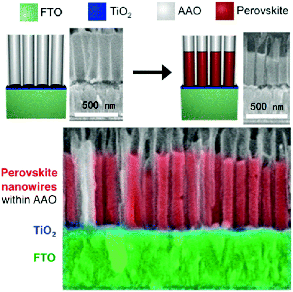 | ||
| Fig. 12 The MAPbI3 nanowire arrays prepared in the AAO tubes. Reprinted with permission from ref. 222. Copyright (2016) American Chemical Society. | ||
Also the morphology controlled design of solar cell scaffolds is frequently discussed in the literature, since it dictates the morphology of the absorbing halide perovskite layer and the contact to the working electrodes.223,224 In 2016 Lee et al. compared the solar cell efficiencies for which either 0D (spherical) silica particles or 1D (rod-like) silica particles with aspect ratios of 3 and 5 were used as scaffold. The authors observed that 1D silica particles with an aspect ratio of 5 increase the solar cell efficiency from 11.85% (in the case of 0D silica particles) to 13.04%. Based on photoluminescence lifetime data, the increased efficiencies were attributed to the improved contact between the halide perovskite and the electron extraction layer.224
For nanoscale halide perovskites, the optoelectronic properties strongly depend on the morphology. As the particle size increased, the absorbance and emission wavelength shifted to longer wavelength along with the extension of the luminescence lifetime. As a result, the stability and control of the morphology has wide implications in the field of halide perovskite.
5. Structural properties of microscale to macroscale halide perovskites
It is well-known that light displays wave-particle duality. When a photon is absorbed by the halide perovskite, charge carriers are being generated immediately, followed by their diffusion to opposite directions. At the nanoscale, the halide perovskites interact with light mainly in terms of particles. Nevertheless, halide perovskites can also interact with light in terms of waves. Because the band gap of halide perovskites can be adjusted between 400 and 800 nm, the hierarchical structure with periodicities from microscale to macroscale will be interesting for enhancing the visible light–perovskite interaction in terms of waves. In the following section, typical hierarchical structures, their synthesis protocols and their unique properties will be discussed.5.1 Periodically arranged halide perovskites
For optoelectronic devices, patterned materials may display enhanced performances or additional functionalities. Generally, a uniform thin film of the perovskite is desirable for optoelectronic devices. Patterned arrangements can satisfy this requirement. Moreover, patterned arrangements can provide wave-guiding and improved light–matter interaction for flexible and semi-transparent devices. By virtue of chemically gas-assisted focused-ion beam (GAFIB) etching, Ooi, Alias and coworkers225 fabricated halide perovskites into a subwavelength grating reflector with sub-micro periodic patterning of high uniformity in order to enhance light trapping and absorption (Fig. 13a). XeF2 and I2 were specifically selected as the chemical precursors for GAFIB etching. In the presence of I2, the etched volume, the sputtering yield and the enhancement factor are higher than those in the presence of XeF2 and those without any assisted gas. The absorbance spectrum, which is consistent with simulations, demonstrated an enhancement of >20% in terms of light absorption by integrating a sub-micro absorber on the perovskite material. Unfortunately, the attenuation of photoluminescence was observed. Due to the inverse relationship between temperature and solubility, Kaehr, Chou and coworkers226 utilized laser radiation to induce local temperature gradients and thus local crystallization of MAPbX3 (X = Cl, Br and I) at specific positions of the substrate, to obtain a patterned material via so-called laser direct write (LDW) (Fig. 13b). TEM micrographs showed that the generated crystals were highly crystalline. After optimization, concentrations above 1.5 M can be used for patterning MAPbBr3. Time-resolved photoluminescence measurements showed similar transport properties of LDW perovskites and single crystals grown from solution. Further Raman spectroscopy proved the damage of the perovskite surface, which will be harmful for optoelectronic properties of halide perovskites and propel the development of other techniques to prepare patterned halide perovskites. | ||
| Fig. 13 (a) Schematic representation of GAFIB and the SEM images of the patterned MAPbI3; reprinted with permission from ref. 225. Copyright (2016) American Chemical Society. (b) Laser-induced crystallization of MAPbBr3 and the SEM images of the obtained crystals. Reprinted with permission from ref. 226. Copyright (2016) American Chemical Society. | ||
Moreover, the LDW protocol can be used on interdigitated microelectrode arrays to fabricate micro-photodetectors, which exhibit a linear response to irradiance with a strong on/off ratio but also strong hysteresis. The protocol provides a straightforward route for the design, iteration and production of perovskite-based devices. However, the direct patterning is not precise enough for other optoelectronic purposes and may deteriorate the halide perovskite material. Consequently, there is a high motivation to pattern halide perovskite materials more precisely.
Imprinting lithography can be used to pattern halide perovskite materials with a higher precision. The imprinting lithography can be classified as soft imprinting and hard imprinting. In the case of soft imprinting, the precursor solution is deposited on the substrate, followed by the deposition of a soft mold. The mold is removed after annealing of the solution. In the case of hard imprinting, the precursor solution is annealed before a hard mold is used to imprint the pattern on the film (Scheme 3). The first example of a thus patterned halide perovskite was reported by Lin and Han in 2003.227 The PDMS stamps fabricated by casting PDMS on silicon masters with desired patterns were deposited on the silicon substrate and the channels of the stamps were filled with the precursor solution of phenylethylammonium (PhE) lead iodide due to capillary forces. By controlling several parameters of the PDMS molds, patterned film stripes with width from 0.8 to 50 μm were obtained and displayed strong green luminescence after the solvent slowly evaporated.
 | ||
| Scheme 3 Soft and hard imprinting lithography for the preparation of patterned perovskite films. | ||
Park and coworkers228 utilized patterned elastomeric poly(dimethylsiloxane) (PDMS) molds to pattern MAPbBr3 and MAPbI3 on different substrates such as SiO2, Au, ITO, FTO and Al2O3 with periodic lines, squares and hexagons via solvent-assisted gel printing (SAGP). A series of factors including solvent and concentration of the precursor solution, imprinting pressure, time and temperature implicated the quality of the film (Fig. 14). The DMSO strongly coordinates with Pb2+ and thus slows down the crystallization process, rendering the film to be in the gel state, which is desirable for fabricating diverse patterns of the film. A concentration of 30 wt% was ideal to avoid unfilled and overfilled patterns of the PDMS line mold. To get defect-free patterned perovskites, the imprinting process was optimized with a pressure of 25 kPa at 80 °C for 15 min. The patterned films can be used as photodetectors and display a pseudo-ohmic response to laser excitation. Moreover, combined with the conventional detachment and transfer printing, the SAGP provided a broader choice of substrates.
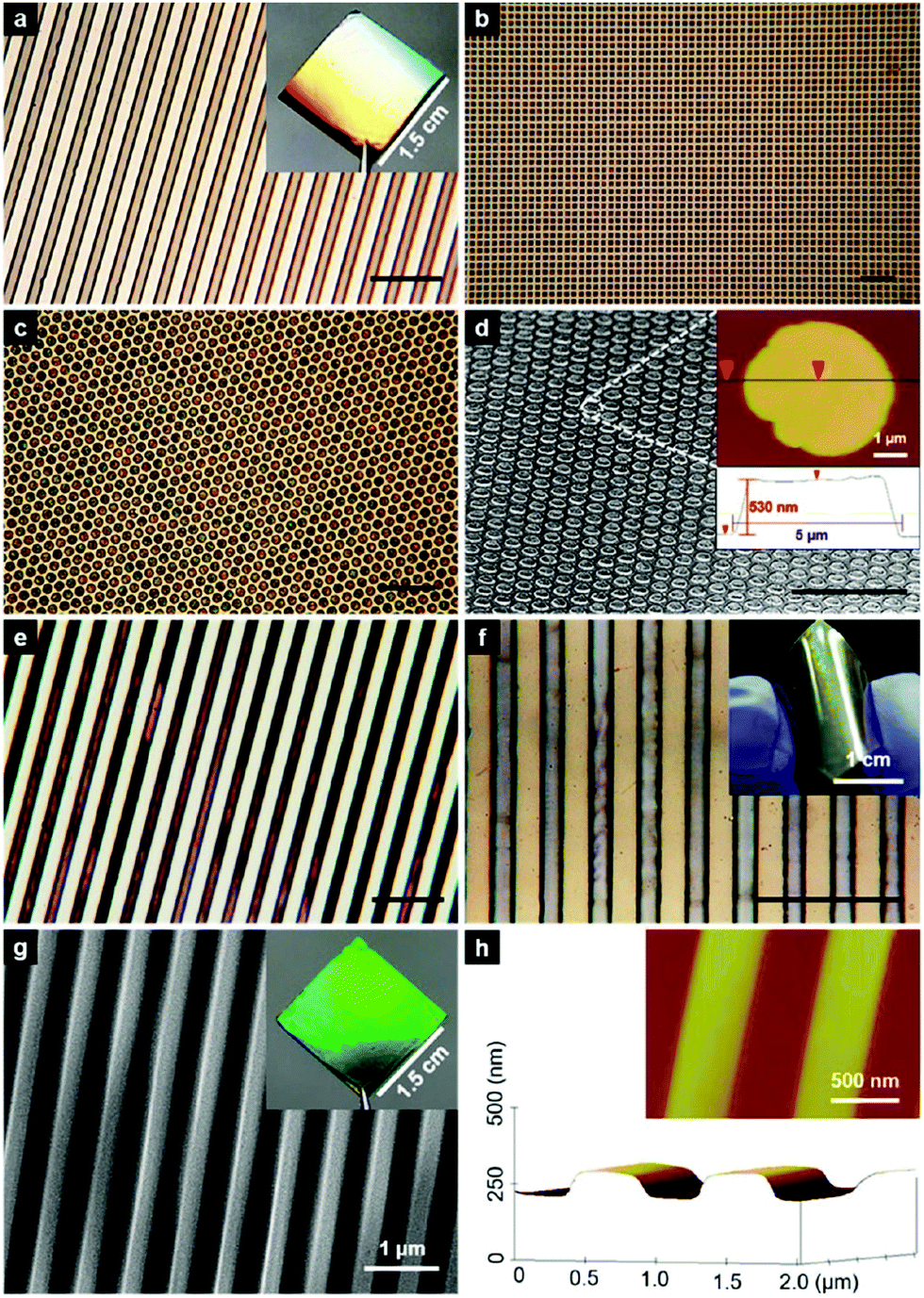 | ||
| Fig. 14 SEM images of the patterned MAPbBr3 films with periodic lines (a), squares arrayed with p4mm symmetry (b), hexagons with p6mm symmetry (c), circles arrayed with p6mm symmetry in a tilted view (d). Bright-field optical images of micropatterned MAPbI3 films with periodic lines (e) and MAPbBr3 line patterns printed on a PET substrate (f). SEM images and AFM images in height contrast of MAPbBr3. Scale bar: 30 μm in (a–f). A field-effect SEM image (g) and a TM-AFM image (h) in height contrast of MAPbBr3 line-pattern of 400 nm in width. Reprinted with permission from ref. 228. Copyright (2016) American Chemical Society. | ||
Choy and coworkers28 also patterned the perovskites with periodic lines (735 nm and 1500 nm interval) using soft PDMS molds with the help of methylamine gas. The conventional MAPbI3 film was exposed to methylamine to generate transparent CH3NH3PbI3·CH3NH2, which was converted back into perovskite by annealing at 100 °C. The PDMS mold was lifted off and the pattern of the mold was imprinted on the perovskite film. SEM micrographs showed that the grain boundaries of the perovskite film disappeared after the direct nanopatterning approach, indicating an improvement of crystallinity, which was also confirmed by the enhancement of the reflection intensity of the XRD measurement. Moreover, the observed enhanced absorption and emission intensities were attributed to the improved crystallinity and the periodic structure. The authors also integrated the periodic structure and the planar perovskite film into light-emitting diodes. The radiance of the device with periodic lines of 735 nm interval (0.53 W m−2 sr−1) is almost two-times of that in the planar LED (0.29 W m−2 sr−1). Thus, the patterned arrangement improves the emission and decreases the emission threshold. Silicon-based molds with nanopillar and nanograting structures can also be used as hard molds to pattern perovskite films under 7 MPa at 100 °C for 20 min.229
Microscopic images and diffraction analysis show that the crystallinity and the surface roughness are greatly improved during the imprinting process. Moreover, the reflectance for the whole spectrum and the transmission in the wavelength range of 550 to 800 nm were reduced. Consequently, a proper mold nanostructure design can enhance the optical absorption, which was evidenced by the improvement of the spontaneous emission properties. The photoluminescence lifetimes of the imprinted perovskite thin film were longer than that of the pristine films. To evaluate the optoelectronic performance of the nanograting perovskite films, they were fabricated into a photodetector (nanograting-PSPD). The obtained photodetector displayed a responsivity of 3.23 A W−1, which is much higher than that of thin film perovskite photodetectors (0.16 A W−1) when illuminated at 466 nm. Moreover, the responsivity of the nanograting-PSPD (24.1 A W−1) is 200 times that of the commercial Si photodetector (0.12 A W−1) under the irradiance of 2 nW cm−2. When illuminated at 635 nm, the responsivity of the nanograting-PSPD is over 30 times that of the thin film photodetector and 20 times that of the commercial Si photodetector under the irradiance of 1 μW cm2.
5.2 Halide perovskite photonic crystals
In the photonic crystal morphology, the periodic alternating areas of low and high refractive index induce the formation of a photonic stopband around a specific wavelength. The group velocity of the light at the edge of the stopband can decrease, which is called “slow photon effect”. The photonic stopband can guide the wave propagation and enhance the out-coupling of light emitting diodes. The slow photon effect can enhance the absorbance of the material and thus improve the performance of optoelectronic devices. 3D photonic crystals (PCs) include a series of structures with opal-related morphologies being the most spread ones integrated into optoelectronic materials. As shown in Scheme 4, artificial opal templates can be manufactured by centrifugation,230 drop casting,231 assembly at the gas–solid interface232 and self-assembly in the liquid drop.43 After infiltration of the polystyrene opal template with a halide perovskite precursor solution, subsequent solvent evaporation and template removal, the halide perovskite inverse opal can be prepared as powdered samples, or as multi and single layered films on substrates. | ||
| Scheme 4 The preparation protocols of the artificial template and halide perovskite photonic crystals. | ||
The Tüysüz group230 developed a universal protocol for the preparation of powdered halide perovskite inverse opals (Scheme 4). The artificial opals, assembled from monodispersed polystyrene spheres, were infiltrated by the precursor solution of the halide perovskite in DMSO. The solvent was evaporated under vacuum and the template was removed by toluene. The pore size of the inverse opal can be controlled by the diameters of the polystyrene microsphere between 135 and 550 nm. Moreover, this protocol is not only compatible with different halide compositions of chloride, bromide and iodide but also flexible with different organic cations including methylammonium (MA), formamidinium (FA) and caesium. The photoconductivity of the MAPbI3 inverse opal was higher than that of the bromide analogue. The halide perovskite inverse opal showed features of ionic conductivity while the same material without the hierarchical structure displayed features of electronic conductivity. Furthermore the Tüysüz group showed that the colloidal crystal templating approach can be utilized to prepare more active halide perovskite photocatalysts as a result of the higher surface area and reduced charge carrier diffusion pathways.36 However, a photonic stopband was not observed in the powdered halide perovskite inverse opals because the long-range order was destroyed during template removal and the powdered materials possess a random orientation of the photonic crystal. Later, Schünemann et al.231 used polystyrene spheres, synthesized via surfactant-assisted polymerization, to prepare artificial opal films on different substrates, which display pronounced photonic stopbands (Scheme 4). The stopband showed a clear dependence of the center wavelength on the incident angle of light due to Bragg diffraction. The inverse opal films preserve the ordered arrangement over a large scale, which is evidenced by the distinctive photonic stopband and the angle-dependent photoluminescence of the film. The stopband position, the thickness and the band gap of the film can be manipulated by the diameters of the polystyrene microsphere, the amount of the polystyrene microsphere, and the halide composition, respectively. More interestingly, the ordered arrangement of the halide perovskite can be used as the cavity to generate a distributed feedback (DFB) laser when the photonic stopband overlaps with the band gap of the halide perovskites. MAPbBr3 inverse opal thin films prepared from 210 nm diameter PS microspheres displayed laser emission with a threshold of 1.6 mJ cm−2 and a FWHM of 0.15 nm under nanosecond pulsed excitation.233
Later, Tüysüz and coworkers43 prepared a series of macroscale composites from photonic crystal beads (PCBs) and halide perovskites and directly observed the slow photon effect (Scheme 4). To prepare PCBs, a drop of the aqueous suspension of the polystyrene microspheres was immersed into silicon oil. As the water evaporated slowly, the microsphere assembled into PCBs. The photonic stopband correlated with the diameter of the microsphere and the diameter of the photonic crystal beads can be controlled by the amount of the microsphere in the suspension. The reflectance spectrum of the PCB/halide perovskite composite displayed both the electronic band gap of the halide perovskite and the photonic stopband of the PCBs, indicating that the ordered arrangement was preserved during the infiltration and drying process. Photoluminescence spectra showed that the emitted light was trapped in the photonic crystal beads when the band gap and stopband overlapped with each other. Moreover, enhanced photoluminescence intensities were observed at the red edge of the stopband, whereas diminished intensities were observed at the blue edge of the stopband, which can be attributed to localization of light in the high and low index media (i.e. the halide perovskite and polystyrene), respectively.
Following the same protocol, Chen and coworkers232 also used polystyrene microspheres as a template to prepare an artificial opal film on the surface by spin-coating (Fig. 15b). After infiltration and template removal, a series of 2D halide perovskite photonic crystal films were integrated into a solar cell and they displayed angle-dependent reflectance phenomena due to Bragg diffraction. The structure of the film can be adjusted by the diameter of the polystyrene microsphere between 100 nm and 2 μm. The bandgap of the film can be controlled by the different constituents of the halide or of the organic cation. In the application of solar cells, the photonic crystal film would improve the performance by enhancing light absorbance and prohibiting the direct contact between electron and hole transporting layers. The solar cells with photonic crystal architecture films displayed an inferior performance, which can be attributed to the low volume fraction of the light absorbing layer as well as the trade-off between color and photocurrent generation. Considering that the slow photon effect and the enhanced properties of the photonic crystal structure require precise regulation, the performances of the solar cells are inspiring because the architecture of the device can be further optimized. Unlike for solar cells, halide perovskite photonic crystal films showed high performances as photodetectors (Fig. 15c).
 | ||
| Fig. 15 (a) Schematic representation of halide perovskite inverse opal on the surface; (b) SEM images and cross-section images of monolayer inverse opal; reprinted with permission from ref. 232. Copyright (2016) American Chemical Society. (c) SEM images of the MAPbX3 nanobowls (X = Cl, Br and I). Reprinted with permission from ref. 234. Copyright © 2017 Wiley-VCH Verlag GmbH & Co. KGaA, Weinheim. | ||
Qi et al.234 prepared a monolayer photonic crystal on a substrate by using polystyrene microspheres. Similar to the aforementioned examples, the replica also preserved the ordered arrangement after infiltration and template removal. The roughness of the substrate displayed implications for the final morphology. When the flat silica surface was used, the replica displayed a netlike morphology. When rough fluorine doped tin oxide (FTO) electrodes were used, the replica display an ordered arrangement of nanobowls. Compared with the compact film, the XRD diffraction patterns of the nanonets and the nanobowls displayed sharper reflections indicating higher crystallinity, which was attributed to the slow evaporation of the solvent, and thus the slow crystallization in the presence of polystyrene microspheres. Moreover, the nanonet/nanobowl arrays displayed better light absorbance and lower light reflectance than the compact films due to multiple light scattering and graded refractive index profiles at the perovskite–air interface. Furthermore, the charge carriers can be transported along the walls of the nanonet under bias owing to the long diffusion length of the halide perovskite. As a result of these advantages, the nanonet photodetector displayed a fast photo response, a higher responsivity and better stability than the compact film.
Even macroporous halide perovskite films without highly ordered arrangements would benefit semitransparent devices in the applications of integrated photovoltaics and tandem cells. Kuang and coworkers235 fabricated a series of solar cells with macroporous halide perovskite films as light absorber layers. Polystyrene microsphere diameters of 200, 400 and 600 nm were used to control the pores in the film. The polystyrene microspheres are beneficial to eliminate the trap site and thus enhance the crystallinity in the perovskite film, which is supported by the sharp XRD reflections, longer charge carrier lifetime, shorter charge transport lifetime, smaller resistance between the hole transfer layer and the perovskite film, and larger resistance of the recombination process than the compact perovskite film. Among macroporous perovskite films, the film prepared from 400 nm polystyrene microspheres displayed the best crystallinity and the highest absorbance with the best device performance.
Besides the aforementioned chemical lithography, photonic crystal (PC) structures can also be prepared by thermal imprint lithography (TIL). Inspired by the band edge mode of the 2D photonic crystal structure, Jeon and coworkers236 fabricated PC lasers with MAPbI3. The square lattice air-hole pattern was generated by electron-beam lithography on the nominal layer of SiO2 (1 μm) and Si3N4 (140 nm). Subsequent pattern transfer down to the Si3N4 layer was accomplished by a selective reactive-ion etching. The perovskite precursor in DMSO was deposited on the structured substrate in a N2-filled glovebox with a diethyl ether dripping protocol. According to the band structure, two kinds of PC patterns were prepared for vertical lasing emission from the Γ-point band edge mode (aΓ = 345 nm; ϕΓ = 150 nm) and for lateral lasing emission from the M-point band edge (aM = 345 nm; ϕM = 150 nm). Both lasing emissions display a threshold of ∼200 μJ cm−2. The polarization characterization showed that the Γ-mode displayed isotropic polarization dependence while the M-mode has anisotropic polarization dependence.
Riedl and coworkers reported that 2D photonic crystal perovskite films prepared by thermal imprint lithography can be applied as a semiconductor laser.237 After patterning of the stamp, the pattern was transferred onto the pristine perovskite layer at 100 °C under 100 bar. The grain size, roughness, and lifetime of the perovskite layer were changed from 180 to 290 nm, 18.7 to 4.9 nm and 12.3 to 21.4 ns, respectively. When the 2D photonic crystal served as a resonator, laser light was coupled out in the direction normal to the surface and the emission wavelength could be tuned between 778.8 and 800.8 nm by controlling the perovskite layer thickness. Due to the improved crystallinity and the smoothing effect of the TIL protocol, the threshold of the laser is as low as 3.8 μJ cm−2 and the stability of the laser is more than 8 h.
5.3 Halide perovskites from patterned substrates
Another protocol for making ordered halide perovskites is to utilize patterned substrates. On the one hand, the substrate is imprinted with special patterns and a thin film of the halide perovskite is deposited on top of the patterned substrate. Later, the pattern of the substrate can enhance the functionality of the perovskite layer (Scheme 5a). On the other hand, the halide perovskite selectively grew with a special pattern due to the interaction between the halide perovskite and the substrate (Scheme 5b). | ||
| Scheme 5 Procedures of patterning the halide perovskite on patterned substrates. (a) A continuous film of the halide perovskite was deposited on the patterned substrate; (b) individual single crystals of the halide perovskite grown on the patterned substrate. | ||
Zhu and coworkers238 patterned halide perovskites with a wettability-assisted photolithography (WAP) process. By virtue of the microstructured photoresist template, the pattern was duplicated on the poly(4-butylphenyl-diphenyl-amine) layer, which was further used as a template to pattern the halide perovskite. The patterned perovskite was incorporated into a solar cell with the configuration glass/FTO/patterned Al2O3/patterned MAPbI3/Spiro-OMe TAD/Au. The device with the patterned structure showed a 44% coverage of the perovskite on the compact TiO2 surface and displayed a PCE of 6.55%, a JSC of 9.83 mA cm−2, a FF of 0.66 and a VOC of 1.01 V. The protocol is also feasible to fabricate inverted devices with the structure glass/FTO/Cu:NiOy/patterned Al2O3/patterned MAPbI3 (410 nm)/PC61BM/ZnO/silver nanowires (Ag NWs)/ZnO. The perovskite coverage of the patterned devices was 44% and the average visible transmittance (AVT) was 62.4% when a 300 nm thick perovskite film was deposited. The inverted devices displayed a PCE of 2.36%, a JSC of 5.44 mA cm−2, a FF of 0.55 and a VOC of 0.79 V. Furthermore, the perovskite film can be deposited directly on the substrates with specific patterns.
Snaith and coworkers239 fabricated semitransparent perovskite solar cells via colloidal monolayer lithography. Different from the aforementioned macroporous halide perovskite films,235 silicon dioxide and titanium dioxide were prepared as the macroporous scaffold using polystyrene microspheres as the template. The pore size and the height of the scaffold can be tuned by the diameter of the microsphere and/or the concentration of the TiO2 precursors or that of the SiO2 nanoparticles. Followed by coating and infiltration of the scaffold with a perovskite precursor solution, the perovskite domains were precisely controlled. The solar cell with the patterned perovskite films exhibited different levels of AVT (28–47%) and displayed a maximum PCE of 9.5%. The integration of the scaffold increased the shunt resistance and decreased the series resistance of the devices, which suppressed charge carrier recombination between the hole blocking layer and the hole transporting layer and thus resulted in elevated VOC and FF of the solar cells. Besides applications in solar cells, patterned halide perovskite materials have great potential in the application of laser. The common cavity modes of halide perovskite lasers are presented in Fig. 16. For instance, single crystalline halide perovskite platelets and rods can realize laser emission from whispering-gallery cavity modes and Fabry–Pérot cavity modes, respectively.
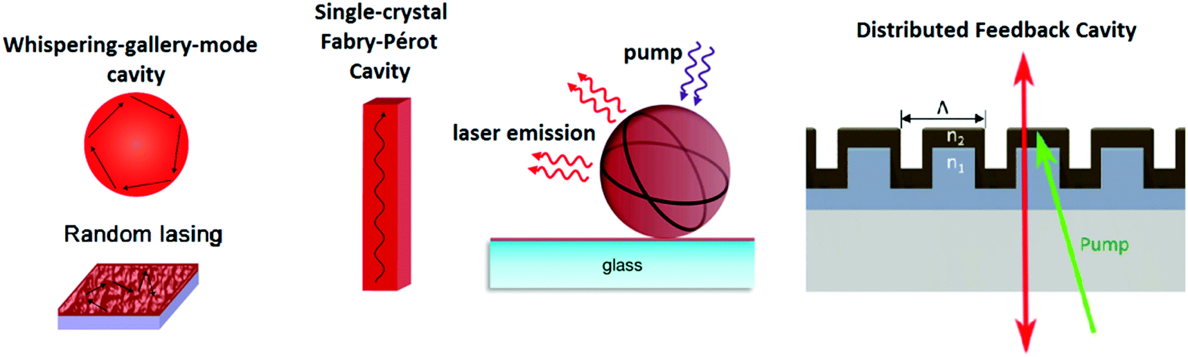 | ||
| Fig. 16 The reported cavity modes of the halide perovskite. Reprinted with permission from ref. 30. Copyright © 2016, Springer Nature; reprinted with permission from ref. 240. Copyright (2014) American Chemical Society; reprinted with permission from ref. 241. Copyright © 2016 Wiley-VCH Verlag GmbH & Co. KGaA, Weinheim. | ||
It is challenging to precisely control the size and shape of the single crystalline halide perovskite. As an alternative protocol, the amplified spontaneous emission can also be realized by depositing polycrystalline halide perovskites on the substrate with specific morphology. Sargent and coworkers240 utilized MAPbI3 coated SiO2 microspheres as the resonator to realize lasing from whispering-gallery modes. Atomic layer deposition (ALD) was used to deposit lead sulfide on the surface to obtain a thin film with constant thickness. Later, the PbS was exposed to iodine gas and converted to PbI2, which was immersed into a MAI solution to obtain MAPbI3. The prepared planar MAPbI3 film displayed an absorption coefficient at 1.58 eV of 3100 ± 830 cm−1 and an estimated gain of 125 ± 22 cm−1. When a silica sphere (d = 52 μm) was used as resonator, a clear threshold was observed at a pump fluence of 75 ± 11 μJ cm−2. The Q-factor of the resonator was conservatively estimated to be on the order of 103.
Riede, Snaith and coworkers241 imprinted grating lines with different periodicities (Λ) from 370 nm to 440 nm on a polymeric resist coated on a glass substrate to prepare a DFB cavity. The precursors, PbCl2 and MAI, were deposited on the patterned substrate with areas from 0.27 cm2 up to 1.6 cm2 for introducing 2D in-plane optical structuring of perovskite films. The fluence thresholds of the amplified spontaneous emission (ASE) peaks are 0.32 (Λ = 400 nm), 0.54 (Λ = 410 nm) and 2.11 (Λ = 420 nm) cm−2 pulse−1, respectively. The ASE peaks with different periodicities localized at 779 nm for Λ = 400 nm, 784 nm for Λ = 410 nm and 793 nm for Λ = 420 nm, respectively. The linewidths of the ASE peak narrowed as the excitation fluences increased and a redshift of the ASE peak with increasing periodicity was observed. All of the presented approaches of halide perovskite DFB lasers demonstrate lasing emission via optical pumping. However, for applications it would be necessary to prepare halide perovskite lasers that can emit laser radiation upon electrical pumping, which will have a multitude of commercial applications including sensors, displays, guidance systems and lab-on-chip technology, but have not yet been achieved.
Giebink and coworkers242 deposited a 50 nm Au layer and a 15 nm Al2O3 layer between a Si grating and a MAPbI3 film. The thresholds of the laser were 91 ± 2 and 40 ± 5 μJ cm−2 when pumped under 355 and 532 nm, respectively. The laser profile displayed a FWHM of 1.1 nm and was strongly transverse-electrically polarized, which is characteristic of second-order DFB lasers. At 160 K, the threshold dramatically decreased to 3.0 ± 0.4 μJ cm−2 due to the increased radiative recombination rate and decreased Auger loss. When the fluence was set at 5.0 ± 0.2 kW cm−2 with a repetition rate of 2 MHz, the laser action died for durations longer than 25 ns. This phenomenon was attributed to gain losses under photoexcitation, resulting from the increased dielectric screening between carriers and the rotational freedom of the MA cation. Although more efforts are required to interpret the lasing mechanism, the DFB lasers display potential for electrically pumped lasing.
With the same strategy, Brenner and coworkers243 deposited a MAPbI3 film via solution-casting to fabricate a DFB laser on top of low-cost polymeric gratings with periodicities of 370 and 380 nm. The threshold of the ASE for the planar film was 190 μJ cm−2 and that of the laser for the film on a grating (Λ = 370 nm) was 120 μJ cm−2. The laser peak centered at 786.5 nm displayed a FWHM of less than 0.2 nm. The intensity of the ASE on a planar film did not change as a linear polarizer between the sample and the detector rotated. In contrast, the intensity of the lasing emission was completely blocked by the polarizer set at 170° and 350°. This observation confirmed the laser emission due to its linearly polarized output. Additionally the obtained laser was stable for 15 h under the fluence of 270 μJ cm−2, which is promising for short-lived disposable devices.
2D photonic crystals provide in-plane distributed optical feedback while being capable of further enhancing light–matter interaction. By precisely tuning the stopband of the photonic crystal and the bandgap of the active medium, the slow photon effect can be achieved, which can be deployed for semiconductor lasers. Nurmikko and coworkers244 utilized electron beam writing and inductively coupled plasma reactive ion etching (ICP-RIE) to pattern substrates with 2D photonic crystal structures. The periodic pitch (Λ) and pillar radius to pitch ratio (r/Λ) can be adjusted to optimize the photonic crystal structure for lasing. MAPbI3 films with a thickness of 128.7 ± 13.9 nm were prepared by spin-casting a precursor in DMSO with a controlled toluene dripping protocol. As Λ increased from 430 to 460 nm, the lasing wavelength shifted from 768.4 to 795.8 nm. The thresholds of the laser with Λ = 430, 440, 450 and 460 nm in the photonic crystal were 141.3 ± 3.2, 79.7 ± 4.5, 68.5 ± 3.0 and 82.6 ± 4.4 μJ cm−2, respectively. The lifetime of the spontaneous emission was 5.44 ± 0.06 ns and that of the lasing decreased to 112.8 ± 9.8 ps. The polarization characteristics of the laser showed a linearly polarized output with the degree of polarization, which indicated the finite deviation from perfect hexagonal symmetry. The stability of the laser can be improved from 10 min to 70 min by depositing one layer of PMMA as a protecting layer. Due to the well-defined spatial output, a 4 × 4 microlaser array was prepared and demonstrated the potential applicability in high brightness displays, 3D modulated projection, etc. Although the property of the halide perovskites can be improved by depositing the film on a patterned substrate, single crystalline materials are attracting more and more attention. In one aspect, single crystalline halide perovskite materials display better optoelectronic properties than the polycrystalline materials due to the lower trap density and fewer crystal boundaries. In another aspect, the patterned perovskite material will be beneficial for flexible electronic devices, and thus extend the applicability. Consequently, the prospect of substrate-controlled growth of patterned perovskite single crystals is a topic of intense research interest.30 However, it is highly challenging to simultaneously control both the size and shape of the single crystalline halide perovskites, not to speak of another additional patterned arrangement. Up to now, the patterns were imprinted on the substrate by controlling the wettability and the single crystalline materials were obtained by post-synthetic conversion of highly crystalline precursors or slow crystallization of precursor solution. The post-synthetic conversion is a powerful protocol to prepare patterned single crystalline perovskite materials. Duan and coworkers245 combined the self-assembly process and lithography process to pattern periodic arrays of hydrophilic areas on the hydrophobic surface (Fig. 17). PbI2 can nucleate and grow into PbI2 microplates on the hydrophilic area, which was monitored by SEM investigations. The size of PbI2 can be tuned by the growth time and the periodicity of the pattern. On exposure to the MAI vapor in a tube furnace, PbI2 microplates were converted to MAPbI3 along with the preservation of both morphology and crystalline quality. The XRD and TEM studies confirmed the single-crystal-to-single-crystal transformation. Absorption and photoluminescence spectra displayed a big shift from 525 and 522 nm to about 800 nm, respectively.
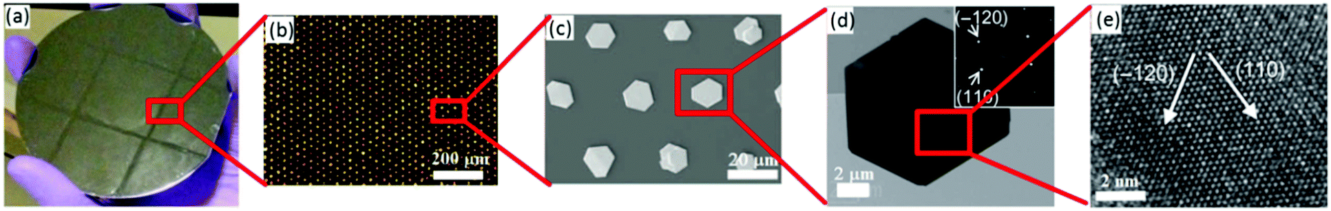 | ||
| Fig. 17 Photograph (a), optical image (b), SEM images (c), TEM (d) and high resolution TEM (e) images of patterned PbI2 single crystals on the silicon substrates. Reprinted with permission from ref. 245. Copyright © 2015, American Association for the Advancement of Science. | ||
The approach can also be applied to gold electrodes to prepare two-probe devices, which exhibited a responsivity of 7 A W−1 with a corresponding photocurrent gain of ∼18. After a preliminary optimization, a photoresponsivity of ∼7 A W−1 and a photocurrent gain of ∼100 were obtained. The field effect electron mobility can reach up to ∼2.5 cm2 V−1 s−1 (backward sweep) and ∼1 cm2 V−1 s−1 (forward sweep). Moreover, the approach is scalable, which opened up the opportunities to explore perovskite arrays for electronic and optoelectronic systems. Due to van der Waals interactions, halide perovskites can be stacked onto graphene, boron-nitride (BN), and transition metal dichalcogenides (TMDs). Large-size 2D monolayers are prepared as inorganic components and epitaxial growth of highly crystalline PbI2 nanoplatelets on prefabricated 2D substrates is performed via a physical vapor deposition (PVD) process. The PbI2 crystals are then converted into the perovskite by reacting with MAI under vacuum, forming organic perovskite MAPbI3/2D solids (Fig. 18).246
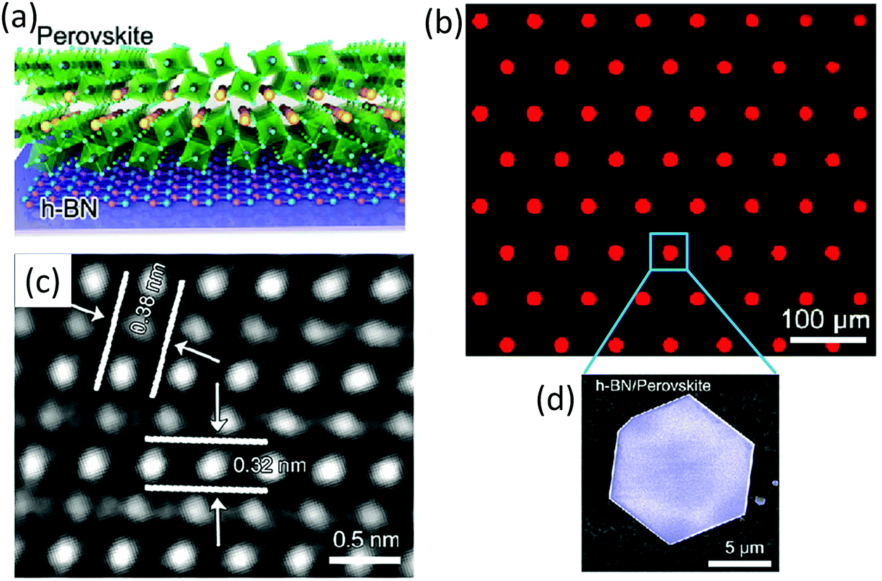 | ||
| Fig. 18 Schematic representation (a) and optical images (b) of MAPbI3 crystals on the born-nitride surface. (c) TEM images of MAPbI3 single crystals; (d) SEM images of perovskite on h-BN. Reprinted with permission from ref. 246. Copyright © 2015 Wiley-VCH Verlag GmbH & Co. KGaA, Weinheim. | ||
Following this protocol, Sum, Liu and coworkers247 deposited one single atomic layer of boron-nitride (BN) as a buffer layer on a SiO2/Si substrate. By virtue of photolithography, the BN film was fabricated with various patterns. BN films, serving as an epitaxial intermediary between the substrate and the perovskite, improved the optical confinement and prevented shorts in practical devices. PbI2 nanoparticles nucleated around the edges and defects of the BN film and merged to form highly crystalline platelets. The disappearance of photoluminescence at 520 nm for PbI2 confirmed that the PbI2 was converted to MAPbI3. XRD and TEM investigations demonstrated the single crystalline nature of MAPbI3. The MAPbI3 microplatelets displayed lasing behavior due to the larger effective index of transverse magnetic (TM) mode compared with transverse electric (TE) mode. As the edge length L increased from 8.3, 13.1, 16.8 to 19.6 μm, the main emission wavelength shifted to the lower energy region; the mode spacing decreased from 5.4 to 2.3 nm; while the lasing threshold decreased from 12.8, 10.8, 10.0 and 9.0 μJ cm−2. Moreover, decreasing the edge length and breaking the symmetry of the cavity structure can realize single mode lasing. Besides the post-synthetic conversion, single crystalline halide perovskite materials can also be prepared by direct crystallization from the precursor solution. Su, Wu and coworkers248 developed a strategy of the ‘liquid knife’ to fabricate patterned single crystalline perovskite microplates for laser arrays (Fig. 19). On the silicon wafer with structure written by the laser apparatus, one photoresist layer was deposited. After irradiation and deep reactive-ion etching, the obtained pillar-structured substrate was modified with sidewall-hydrophobicity and top-hydrophilicity, respectively. When the MAPbBr3 precursor solution is deposited on the substrate, the liquid can only localize on the top of pillars due to the hydrophobicity of the sidewalls. As the solvent evaporated, a concave meniscus appeared because the interaction between the solvent and pillar top is stronger than that between the solvent molecules. As a result, the pillar-structured substrate can be used as a liquid knife to split the precursor liquid film into regular microdomains. During the solvent evaporation, the precursor solution slowly crystallized into square microplates. The width of the microplates can be tuned by the size of the pillar top and the height was homogeneous and roughly 0.9 ± 0.1 μm. TEM and XRD characterization demonstrated the cubic structure of the microplates and their single crystalline nature. The microplates displayed an absorption peak at 515 nm and a PL emission at 535 nm. The microplate laser, arising from the transverse magnetic mode, displayed a threshold of 3.5 μJ cm−2 and exhibited two peaks at 553 and 557 nm with FWHM of 1.7 and 1.2 nm, respectively. Spatially resolved photoluminescence measurements showed that the sharp and strong intensity at the corners of the microplates, which is consistent with the longer lifetimes of the fluorescence at the sidewalls and centers than at the corners of microplate. These observations showed that the microplates showed that the total internal reflection of microplate and it is propagated in the inner body of the microcavity. As the size of the microplates increased, the lasing output split into two or more peaks due to the appearance of other resonance modes. Moreover, the precursor liquid can be on-demand split into patterned domains by controlling the pattern of the pillar-structured substrate and is compatible with bandgap engineering between 510 nm and 780 nm by adjusting the halide composition.
 | ||
| Fig. 19 (a) Schematic representation of the liquid knife; (b and c) optical images of the MAPbBr3 single crystals on the substrate. (d) TEM images of the MAPbBr3 single crystal; (e) PL intensity mapping of the MAPbBr3 single crystals on h-BN. Reprinted with permission from ref. 248. Copyright © 2016 Wiley-VCH Verlag GmbH & Co. KGaA, Weinheim. | ||
As for all-inorganic halide perovskites, it is also possible to fabricate patterned multicolor laser arrays. Fu and coworkers249 fabricated PDMS cylindrical-hole-template (CHT) by casting PDMS against a silicon mold with convex cylinders. The PDMS-CHT was brought into contact with a thin layer of CsX·PbX2 solution (X = Cl and Br). Under a mild pressure, the stock solution (0.2 M in DMF) was driven into the void space of PDMS-CHTs. The solvent of the stock solution in the cylindrical pores slowly evaporated along with the nucleation and growth of the CsPbX3 microdisks (MDs). The CsPbCl3 MDs are quite uniform with a side length of 2.5 ± 0.3 μm and a thickness of 0.6 ± 0.2 μm, which can be tuned by the diameters of the cylinder and the distance between the cylinders in the template. By adjusting the halide composition, a series of CsPbClxBr3−x orthorhombic single crystalline MDs can be prepared, as evidenced by XRD, TEM and absorption spectroscopy studies. The MDs exhibited low lasing thresholds of 3–12 μJ cm−2 and displayed lasing behavior at 425, 460, 495, and 540 nm, respectively. Time-resolved PL measurements revealed lifetimes of 3.56 ± 0.06 ns for spontaneous emission and 21 ± 5 ps for lasing emission. The vapor–solid reaction can also be used to adjust the halide composition by controlling the reaction time. The diverse structural parameters and laser properties of the halide perovskites are summarized in Table 3.
6. Outlook and summary
In summary, structural factors including nanoscale morphology, grain size, patterned arrangement, and hierarchical structure play an important role not only in the fundamental optoelectronic properties of halide perovskites but also in the performance of devices made from this intriguing material. However, structural control of halide perovskites is highly challenging since many factors should be considered such as crystal structure, degree of crystallinity and material stability. In addition, for applications in optoelectronic devices, consideration should be given to the working principle of property tenability, the compatibility of device fabrication and the production cost. First, stability is one of the key concerns for the community.3 Halide perovskites display poor stability in terms of chemical composition, crystal structure and morphology. As a result, the preservation of the structural factors is highly challenging. Encapsulation is widely used to improve the stability. Silicon oxide, phosphine derivatives and organic compounds were used as protecting layers to enhance the stability of nanomaterials and bulk materials. The stability has been enhanced and the protected materials even display robust stability in aqueous solutions. However, the most desirable protecting layer should be transparent, hydrophobic and conductive in order to be compatible with the application as optoelectronic devices while enhancing the stability. Moreover, it will be even more challenging to improve the stability of the material with a specific pattern and hierarchical structure due to its higher surface area and more complex structure. Secondly, the development of novel morphologies is desirable for optoelectronic devices.The application of halide perovskites mainly focuses on the solar cell and other optoelectronic devices. Due to the wave-particle duality of light, the light–matter interaction can be improved by both wave characteristics and particle characteristics. The performance enhancement of the inverse opal morphology utilizes the wave characteristics of light. Consequently, the specific structure, which can enhance the performance in the optoelectronic device, may be integrated into the optoelectronic devices. The enhanced performance, in turn, allows realizing the same performance with less amount of material, which is environmentally friendlier considering the toxicity of lead. Up to now, the morphology of nanoscale halide perovskites is limited to 0D (quantum dots), 1D (nanorods, nanofibers and nanowires) and 2D (nanoplatelets and nanodisks) materials. For micro and macroscale materials, only periodic lines and inverse opal structures were realized. Other novel structures including nanoscale morphology, patterned arrangement and other photonic crystal structures have not yet been achieved and further work in this direction is necessary.
Finally, crystallinity is another important factor that influences the properties of halide perovskites. It is well-known that single crystalline materials display lower trap densities than polycrystalline materials. As a result, crystallinity should be precisely controlled during the material preparation, the device fabrication as well as the application. Although the patterned arrangement of single crystals has been realized recently, it is highly challenging to pattern single crystalline materials on a large scale and/or with low cost. Moreover, it has not yet been possible to prepare highly crystalline halide perovskite materials with special patterns and/or hierarchical structure. Post-synthetic strategies can be a very powerful toolbox to prepare halide perovskite materials. It is feasible not only for the conversion from precursors to the perovskite but also for the halide exchange among halide perovskites with different compositions. The post-synthesis modification of halide perovskites in solution is fast (at minute time scales) but without morphology preservation. Gas–solid reactions have been achieved for both nanoscale materials and materials with hierarchical structure while preserving the crystallinity and structure. In principle, highly crystalline halide perovskite materials with specific structures can be extended to a series of materials with different compositions (band gaps) while preserving the same structure and crystallinity by virtue of the gas–solid post-synthetic protocol.
Although great progress has been made in the field of halide perovskites, tremendous efforts are still required for the commercialization of halide perovskites for optoelectronic applications. Due to the relationship between structural factors and the properties, structural factors should be precisely controlled during the material preparation and device fabrication to fulfil the requirements with improved performances.
Conflicts of interest
There are no conflicts to declare.Acknowledgements
This work was supported by the MAXNET Energy consortium of Max Planck Society and the Cluster of Excellence RESOLV (EXC 1069) funded by DFG, Fonds der Chemischen Industrie (FCI). K. C. thanks the Beijing Institute of Technology Research Fund Program for Young Scholars. Open Access funding provided by the Max Planck Society.References
- E. W. McFarland, Energy Environ. Sci., 2014, 7, 846–854 RSC.
- T. A. Faunce, W. Lubitz, A. W. Rutherford, D. MacFarlane, G. F. Moore, P. Yang, D. G. Nocera, T. A. Moore, D. H. Gregory, S. Fukuzumi, K. B. Yoon, F. A. Armstrong, M. R. Wasielewski and S. Styring, Energy Environ. Sci., 2013, 6, 695–698 RSC.
- J.-P. Correa-Baena, M. Saliba, T. Buonassisi, M. Grätzel, A. Abate, W. Tress and A. Hagfeldt, Science, 2017, 358, 739–744 CrossRef PubMed.
- P. Cheng and X. Zhan, Chem. Soc. Rev., 2016, 45, 2544–2582 RSC.
- M. Jørgensen, K. Norrman, S. A. Gevorgyan, T. Tromholt, B. Andreasen and F. C. Krebs, Adv. Mater., 2012, 24, 580–612 CrossRef PubMed.
- F. Di Giacomo, A. Fakharuddin, R. Jose and T. M. Brown, Energy Environ. Sci., 2016, 9, 3007–3035 RSC.
- L. Li, Z. Wu, S. Yuan and X.-B. Zhang, Energy Environ. Sci., 2014, 7, 2101–2122 RSC.
- T. D. Lee and A. U. Ebong, Renewable Sustainable Energy Rev., 2017, 70, 1286–1297 CrossRef.
- S. Mirhassani, H. C. Ong, W. T. Chong and K. Y. Leong, Renewable Sustainable Energy Rev., 2015, 49, 121–131 CrossRef.
- M.-R. Gao, Y.-F. Xu, J. Jiang and S.-H. Yu, Chem. Soc. Rev., 2013, 42, 2986–3017 RSC.
- Q. Zhang, E. Uchaker, S. L. Candelaria and G. Cao, Chem. Soc. Rev., 2013, 42, 3127–3171 RSC.
- X. Liang, S. Bai, X. Wang, X. Dai, F. Gao, B. Sun, Z. Ning, Z. Ye and Y. Jin, Chem. Soc. Rev., 2017, 46, 1730–1759 RSC.
- G. F. Brown and J. Wu, Laser Photonics Rev., 2009, 3, 394–405 CrossRef.
- H. L. Wells, Z. Anorg. Chem., 1893, 3, 195–210 CrossRef.
- D. B. Mitzi, C. A. Feild, W. T. A. Harrison and A. M. Guloy, Nature, 1994, 369, 467–469 CrossRef.
- A. Kojima, K. Teshima, Y. Shirai and T. Miyasaka, J. Am. Chem. Soc., 2009, 131, 6050–6051 CrossRef PubMed.
- P. Gao, M. Gratzel and M. K. Nazeeruddin, Energy Environ. Sci., 2014, 7, 2448–2463 RSC.
- J. Seo, J. H. Noh and S. I. Seok, Acc. Chem. Res., 2016, 49, 562–572 CrossRef PubMed.
- W. E. I. Sha, X. Ren, L. Chen and W. C. H. Choy, Appl. Phys. Lett., 2015, 106, 221104 CrossRef.
- W. S. Yang, B.-W. Park, E. H. Jung, N. J. Jeon, Y. C. Kim, D. U. Lee, S. S. Shin, J. Seo, E. K. Kim, J. H. Noh and S. I. Seok, Science, 2017, 356, 1376–1379 CrossRef PubMed.
- M. A. Green, Y. Jiang, A. M. Soufiani and A. Ho-Baillie, J. Phys. Chem. Lett., 2015, 6, 4774–4785 CrossRef PubMed.
- S. D. Stranks, G. E. Eperon, G. Grancini, C. Menelaou, M. J. P. Alcocer, T. Leijtens, L. M. Herz, A. Petrozza and H. J. Snaith, Science, 2013, 342, 341–344 CrossRef PubMed.
- R. E. Brandt, V. Stevanović, D. S. Ginley and T. Buonassisi, MRS Commun., 2015, 5, 265–275 CrossRef.
- G. Xing, N. Mathews, S. Sun, S. S. Lim, Y. M. Lam, M. Grätzel, S. Mhaisalkar and T. C. Sum, Science, 2013, 342, 344–347 CrossRef PubMed.
- A. Walsh, J. Phys. Chem. C, 2015, 119, 5755–5760 CrossRef PubMed.
- S. Collavini, S. F. Völker and J. L. Delgado, Angew. Chem., Int. Ed., 2015, 54, 9757–9759 CrossRef PubMed.
- S. D. Stranks and H. J. Snaith, Nat. Nanotechnol., 2015, 10, 391–402 CrossRef PubMed.
- J. Mao, W. E. I. Sha, H. Zhang, X. Ren, J. Zhuang, V. A. L. Roy, K. S. Wong and W. C. H. Choy, Adv. Funct. Mater., 2017, 27, 1606525 CrossRef.
- Y.-H. Kim, H. Cho and T.-W. Lee, Proc. Natl. Acad. Sci. U. S. A., 2016, 113, 11694–11702 CrossRef PubMed.
- B. R. Sutherland and E. H. Sargent, Nat. Photonics, 2016, 10, 295–302 CrossRef.
- Y. Zhao and K. Zhu, Chem. Soc. Rev., 2016, 45, 655–689 RSC.
- S. Park, W. J. Chang, C. W. Lee, S. Park, H.-Y. Ahn and K. T. Nam, Nat. Energy, 2016, 2, 16185 CrossRef.
- Y.-F. Xu, M.-Z. Yang, B.-X. Chen, X.-D. Wang, H.-Y. Chen, D.-B. Kuang and C.-Y. Su, J. Am. Chem. Soc., 2017, 139, 5660–5663 CrossRef PubMed.
- K. Chen, X. Deng, G. Dodekatos and H. Tüysüz, J. Am. Chem. Soc., 2017, 139, 12267–12273 CrossRef PubMed.
- J. Hou, S. Cao, Y. Wu, Z. Gao, F. Liang, Y. Sun, Z. Lin and L. Sun, Chem. – Eur. J., 2017, 23, 9481–9485 CrossRef PubMed.
- S. Schünemann and H. Tüysüz, Eur. J. Inorg. Chem., 2018, 2350–2355, DOI:10.1002/ejic.201800078.
- S. Schünemann, M. van Gastel and H. Tüysüz, ChemSusChem, 2018, 11, 2057–2061 CrossRef PubMed.
- C. Muthu, S. R. Nagamma and V. C. Nair, RSC Adv., 2014, 4, 55908–55911 RSC.
- J. H. Kim and S.-H. Kim, Dyes Pigm., 2016, 133, 73–78 CrossRef.
- Q. Dong, Y. Fang, Y. Shao, P. Mulligan, J. Qiu, L. Cao and J. Huang, Science, 2015, 347, 967–970 CrossRef PubMed.
- H. Zhu, Y. Fu, F. Meng, X. Wu, Z. Gong, Q. Ding, M. V. Gustafsson, M. T. Trinh, S. Jin and X. Y. Zhu, Nat. Mater., 2015, 14, 636–642 CrossRef PubMed.
- J.-H. Im, I.-H. Jang, N. Pellet, M. Grätzel and N.-G. Park, Nat. Nanotechnol., 2014, 9, 927–932 CrossRef PubMed.
- K. Chen, S. Schünemann and H. Tüysüz, Angew. Chem., Int. Ed., 2017, 56, 6548–6552 CrossRef PubMed.
- V. Adinolfi, W. Peng, G. Walters, O. M. Bakr and E. H. Sargent, Adv. Mater., 2018, 30, 1700764 CrossRef PubMed.
- L. Mao, H. Tsai, W. Nie, L. Ma, J. Im, C. C. Stoumpos, C. D. Malliakas, F. Hao, M. R. Wasielewski, A. D. Mohite and M. G. Kanatzidis, Chem. Mater., 2016, 28, 7781–7792 CrossRef.
- B. Saparov and D. B. Mitzi, Chem. Rev., 2016, 116, 4558–4596 CrossRef PubMed.
- Y. Hassan, Y. Song, R. D. Pensack, A. I. Abdelrahman, Y. Kobayashi, M. A. Winnik and G. D. Scholes, Adv. Mater., 2016, 28, 566–573 CrossRef PubMed.
- A. Sharenko and M. F. Toney, J. Am. Chem. Soc., 2016, 138, 463–470 CrossRef PubMed.
- G. Kieslich, S. Sun and A. K. Cheetham, Chem. Sci., 2015, 6, 3430–3433 RSC.
- H.-S. Kim, S. H. Im and N.-G. Park, J. Phys. Chem. C, 2014, 118, 5615–5625 CrossRef.
- J. S. Manser, J. A. Christians and P. V. Kamat, Chem. Rev., 2016, 116, 12956–13008 CrossRef PubMed.
- R. X. Yang, J. M. Skelton, E. L. da Silva, J. M. Frost and A. Walsh, J. Phys. Chem. Lett., 2017, 8, 4720–4726 CrossRef PubMed.
- C. C. Stoumpos and M. G. Kanatzidis, Acc. Chem. Res., 2015, 48, 2791–2802 CrossRef PubMed.
- A. Amat, E. Mosconi, E. Ronca, C. Quarti, P. Umari, M. K. Nazeeruddin, M. Grätzel and F. De Angelis, Nano Lett., 2014, 14, 3608–3616 CrossRef PubMed.
- Y. K. a. T. A. H. Mashiyama, J. Korean Phys. Soc., 1998, 32, S156–S158 Search PubMed.
- W. Peng, L. Wang, B. Murali, K.-T. Ho, A. Bera, N. Cho, C.-F. Kang, V. M. Burlakov, J. Pan, L. Sinatra, C. Ma, W. Xu, D. Shi, E. Alarousu, A. Goriely, J.-H. He, O. F. Mohammed, T. Wu and O. M. Bakr, Adv. Mater., 2016, 28, 3383–3390 CrossRef PubMed.
- G. Maculan, A. D. Sheikh, A. L. Abdelhady, M. I. Saidaminov, M. A. Haque, B. Murali, E. Alarousu, O. F. Mohammed, T. Wu and O. M. Bakr, J. Phys. Chem. Lett., 2015, 6, 3781–3786 CrossRef PubMed.
- A. Poglitsch and D. Weber, J. Chem. Phys., 1987, 87, 6373–6378 CrossRef.
- A. Jaffe, Y. Lin, C. M. Beavers, J. Voss, W. L. Mao and H. I. Karunadasa, ACS Cent. Sci., 2016, 2, 201–209 CrossRef PubMed.
- G. A. Elbaz, D. B. Straus, O. E. Semonin, T. D. Hull, D. W. Paley, P. Kim, J. S. Owen, C. R. Kagan and X. Roy, Nano Lett., 2017, 17, 1727–1732 CrossRef PubMed.
- D. Shi, V. Adinolfi, R. Comin, M. Yuan, E. Alarousu, A. Buin, Y. Chen, S. Hoogland, A. Rothenberger, K. Katsiev, Y. Losovyj, X. Zhang, P. A. Dowben, O. F. Mohammed, E. H. Sargent and O. M. Bakr, Science, 2015, 347, 519–522 CrossRef PubMed.
- C. C. Stoumpos, C. D. Malliakas and M. G. Kanatzidis, Inorg. Chem., 2013, 52, 9019–9038 CrossRef PubMed.
- M. Sebastian, J. A. Peters, C. C. Stoumpos, J. Im, S. S. Kostina, Z. Liu, M. G. Kanatzidis, A. J. Freeman and B. W. Wessels, Phys. Rev. B: Condens. Matter Mater. Phys., 2015, 92, 235210 CrossRef.
- A. R. Lim and S.-Y. Jeong, Phys. B, 2001, 304, 79–85 CrossRef.
- M. Rodová, J. Brožek, K. Knížek and K. Nitsch, J. Therm. Anal. Calorim., 2003, 71, 667–673 CrossRef.
- Y. Rakita, N. Kedem, S. Gupta, A. Sadhanala, V. Kalchenko, M. L. Böhm, M. Kulbak, R. H. Friend, D. Cahen and G. Hodes, Cryst. Growth Des., 2016, 16, 5717–5725 CrossRef.
- C. C. Stoumpos, C. D. Malliakas, J. A. Peters, Z. Liu, M. Sebastian, J. Im, T. C. Chasapis, A. C. Wibowo, D. Y. Chung, A. J. Freeman, B. W. Wessels and M. G. Kanatzidis, Cryst. Growth Des., 2013, 13, 2722–2727 CrossRef.
- B. Yang, F. Zhang, J. Chen, S. Yang, X. Xia, T. Pullerits, W. Deng and K. Han, Adv. Mater., 2017, 29, 1703758 CrossRef PubMed.
- F. Chen, C. Zhu, C. Xu, P. Fan, F. Qin, A. Gowri Manohari, J. Lu, Z. Shi, Q. Xu and A. Pan, J. Mater. Chem. C, 2017, 5, 7739–7745 RSC.
- M. Lai, Q. Kong, C. G. Bischak, Y. Yu, L. Dou, S. W. Eaton, N. S. Ginsberg and P. Yang, Nano Res., 2017, 10, 1107–1114 CrossRef.
- S. Dastidar, S. Li, S. Y. Smolin, J. B. Baxter and A. T. Fafarman, ACS Energy Lett., 2017, 2, 2239–2244 CrossRef.
- D. M. Trots and S. V. Myagkota, J. Phys. Chem. Solids, 2008, 69, 2520–2526 CrossRef.
- A. A. Zhumekenov, M. I. Saidaminov, M. A. Haque, E. Alarousu, S. P. Sarmah, B. Murali, I. Dursun, X.-H. Miao, A. L. Abdelhady, T. Wu, O. F. Mohammed and O. M. Bakr, ACS Energy Lett., 2016, 1, 32–37 CrossRef.
- L. Wang, K. Wang and B. Zou, J. Phys. Chem. Lett., 2016, 7, 2556–2562 CrossRef PubMed.
- Q. Han, S.-H. Bae, P. Sun, Y.-T. Hsieh, Y. Yang, Y. S. Rim, H. Zhao, Q. Chen, W. Shi, G. Li and Y. Yang, Adv. Mater., 2016, 28, 2253–2258 CrossRef PubMed.
- M. C. Gélvez-Rueda, N. Renaud and F. C. Grozema, J. Phys. Chem. C, 2017, 121, 23392–23397 CrossRef PubMed.
- Z. Xiao and Y. Yan, Adv. Energy Mater., 2017, 7, 1701136 CrossRef.
- L. Protesescu, S. Yakunin, M. I. Bodnarchuk, F. Krieg, R. Caputo, C. H. Hendon, R. X. Yang, A. Walsh and M. V. Kovalenko, Nano Lett., 2015, 15, 3692–3696 CrossRef PubMed.
- D. J. Slotcavage, H. I. Karunadasa and M. D. McGehee, ACS Energy Lett., 2016, 1, 1199–1205 CrossRef.
- C. G. Bischak, C. L. Hetherington, H. Wu, S. Aloni, D. F. Ogletree, D. T. Limmer and N. S. Ginsberg, Nano Lett., 2017, 17, 1028–1033 CrossRef PubMed.
- C. C. Stoumpos, L. Mao, C. D. Malliakas and M. G. Kanatzidis, Inorg. Chem., 2017, 56, 56–73 CrossRef PubMed.
- J. Even, L. Pedesseau and C. Katan, J. Phys. Chem. C, 2014, 118, 11566–11572 CrossRef.
- A. A. Bakulin, O. Selig, H. J. Bakker, Y. L. A. Rezus, C. Müller, T. Glaser, R. Lovrincic, Z. Sun, Z. Chen, A. Walsh, J. M. Frost and T. L. C. Jansen, J. Phys. Chem. Lett., 2015, 6, 3663–3669 CrossRef PubMed.
- J. M. Frost and A. Walsh, Acc. Chem. Res., 2016, 49, 528–535 CrossRef PubMed.
- A. Zakutayev, C. M. Caskey, A. N. Fioretti, D. S. Ginley, J. Vidal, V. Stevanovic, E. Tea and S. Lany, J. Phys. Chem. Lett., 2014, 5, 1117–1125 CrossRef PubMed.
- Z. Liu, J. Hu, H. Jiao, L. Li, G. Zheng, Y. Chen, Y. Huang, Q. Zhang, C. Shen, Q. Chen and H. Zhou, Adv. Mater., 2017, 29, 1606774 CrossRef PubMed.
- D. N. Dirin, I. Cherniukh, S. Yakunin, Y. Shynkarenko and M. V. Kovalenko, Chem. Mater., 2016, 28, 8470–8474 CrossRef PubMed.
- J. Ding, S. Du, Z. Zuo, Y. Zhao, H. Cui and X. Zhan, J. Phys. Chem. C, 2017, 121, 4917–4923 CrossRef.
- Y. Fang, Q. Dong, Y. Shao, Y. Yuan and J. Huang, Nat. Photonics, 2015, 9, 679 CrossRef.
- S. Shrestha, R. Fischer, G. J. Matt, P. Feldner, T. Michel, A. Osvet, I. Levchuk, B. Merle, S. Golkar, H. Chen, S. F. Tedde, O. Schmidt, R. Hock, M. Rührig, M. Göken, W. Heiss, G. Anton and C. J. Brabec, Nat. Photonics, 2017, 11, 436 CrossRef.
- S. Yakunin, M. Sytnyk, D. Kriegner, S. Shrestha, M. Richter, G. J. Matt, H. Azimi, C. J. Brabec, J. Stangl, M. V. Kovalenko and W. Heiss, Nat. Photonics, 2015, 9, 444 CrossRef PubMed.
- H. Wei, D. DeSantis, W. Wei, Y. Deng, D. Guo, T. J. Savenije, L. Cao and J. Huang, Nat. Mater., 2017, 16, 826–833 CrossRef PubMed.
- M. I. Saidaminov, A. L. Abdelhady, B. Murali, E. Alarousu, V. M. Burlakov, W. Peng, I. Dursun, L. Wang, Y. He, G. Maculan, A. Goriely, T. Wu, O. F. Mohammed and O. M. Bakr, Nat. Commun., 2015, 6, 7586 CrossRef PubMed.
- Y. Dang, D. Ju, L. Wang and X. Tao, CrystEngComm, 2016, 18, 4476–4484 RSC.
- P. K. Nayak, D. T. Moore, B. Wenger, S. Nayak, A. A. Haghighirad, A. Fineberg, N. K. Noel, O. G. Reid, G. Rumbles, P. Kukura, K. A. Vincent and H. J. Snaith, Nat. Commun., 2016, 7, 13303 CrossRef PubMed.
- A. R. Srimath Kandada and A. Petrozza, Acc. Chem. Res., 2016, 49, 536–544 CrossRef PubMed.
- H.-S. Kim and N.-G. Park, J. Phys. Chem. Lett., 2014, 5, 2927–2934 CrossRef PubMed.
- J. M. Ball, M. M. Lee, A. Hey and H. J. Snaith, Energy Environ. Sci., 2013, 6, 1739–1743 RSC.
- V. D’Innocenzo, A. R. Srimath Kandada, M. De Bastiani, M. Gandini and A. Petrozza, J. Am. Chem. Soc., 2014, 136, 17730–17733 CrossRef PubMed.
- H. D. Kim, H. Ohkita, H. Benten and S. Ito, Adv. Mater., 2016, 28, 917–922 CrossRef PubMed.
- C. G. Bischak, E. M. Sanehira, J. T. Precht, J. M. Luther and N. S. Ginsberg, Nano Lett., 2015, 15, 4799–4807 CrossRef PubMed.
- S. Shao, M. Abdu-Aguye, T. S. Sherkar, H.-H. Fang, S. Adjokatse, G. t. Brink, B. J. Kooi, L. J. A. Koster and M. A. Loi, Adv. Funct. Mater., 2016, 26, 8094–8102 CrossRef.
- W. Nie, H. Tsai, R. Asadpour, J.-C. Blancon, A. J. Neukirch, G. Gupta, J. J. Crochet, M. Chhowalla, S. Tretiak, M. A. Alam, H.-L. Wang and A. D. Mohite, Science, 2015, 347, 522–525 CrossRef PubMed.
- G. E. Eperon, V. M. Burlakov, P. Docampo, A. Goriely and H. J. Snaith, Adv. Funct. Mater., 2014, 24, 151–157 CrossRef.
- S. T. Williams, F. Zuo, C.-C. Chueh, C.-Y. Liao, P.-W. Liang and A. K. Y. Jen, ACS Nano, 2014, 8, 10640–10654 CrossRef PubMed.
- W. Yan, Y. Li, Y. Li, S. Ye, Z. Liu, S. Wang, Z. Bian and C. Huang, Nano Res., 2015, 8, 2474–2480 CrossRef.
- K. Yan, M. Long, T. Zhang, Z. Wei, H. Chen, S. Yang and J. Xu, J. Am. Chem. Soc., 2015, 137, 4460–4468 CrossRef PubMed.
- D. T. Moore, H. Sai, K. W. Tan, D.-M. Smilgies, W. Zhang, H. J. Snaith, U. Wiesner and L. A. Estroff, J. Am. Chem. Soc., 2015, 137, 2350–2358 CrossRef PubMed.
- G. E. Eperon, S. D. Stranks, C. Menelaou, M. B. Johnston, L. M. Herz and H. J. Snaith, Energy Environ. Sci., 2014, 7, 982–988 RSC.
- W. Zhang, M. Saliba, D. T. Moore, S. K. Pathak, M. T. Hörantner, T. Stergiopoulos, S. D. Stranks, G. E. Eperon, J. A. Alexander-Webber, A. Abate, A. Sadhanala, S. Yao, Y. Chen, R. H. Friend, L. A. Estroff, U. Wiesner and H. J. Snaith, Nat. Commun., 2015, 6, 6142 CrossRef PubMed.
- C. Wehrenfennig, G. E. Eperon, M. B. Johnston, H. J. Snaith and L. M. Herz, Adv. Mater., 2014, 26, 1584–1589 CrossRef PubMed.
- P.-W. Liang, C.-Y. Liao, C.-C. Chueh, F. Zuo, S. T. Williams, X.-K. Xin, J. Lin and A. K. Y. Jen, Adv. Mater., 2014, 26, 3748–3754 CrossRef PubMed.
- S. Bag and M. F. Durstock, ACS Appl. Mater. Interfaces, 2016, 8, 5053–5057 CrossRef PubMed.
- Q. Zhang, S. T. Ha, X. Liu, T. C. Sum and Q. Xiong, Nano Lett., 2014, 14, 5995–6001 CrossRef PubMed.
- M. V. Kovalenko, L. Protesescu and M. I. Bodnarchuk, Science, 2017, 358, 745–750 CrossRef PubMed.
- X. Li, F. Cao, D. Yu, J. Chen, Z. Sun, Y. Shen, Y. Zhu, L. Wang, Y. Wei, Y. Wu and H. Zeng, Small, 2017, 13, 1603996 CrossRef PubMed.
- M. I. Saidaminov, O. F. Mohammed and O. M. Bakr, ACS Energy Lett., 2017, 2, 889–896 CrossRef.
- K. Hong, Q. V. Le, S. Y. Kim and H. W. Jang, J. Mater. Chem. C, 2018, 6, 2189–2209 RSC.
- Y. Zhang, J. Liu, Z. Wang, Y. Xue, Q. Ou, L. Polavarapu, J. Zheng, X. Qi and Q. Bao, Chem. Commun., 2016, 52, 13637–13655 RSC.
- J. M. Ball and A. Petrozza, Nat. Energy, 2016, 1, 16149 CrossRef.
- R. E. Brandt, J. R. Poindexter, P. Gorai, R. C. Kurchin, R. L. Z. Hoye, L. Nienhaus, M. W. B. Wilson, J. A. Polizzotti, R. Sereika, R. Žaltauskas, L. C. Lee, J. L. MacManus-Driscoll, M. Bawendi, V. Stevanović and T. Buonassisi, Chem. Mater., 2017, 29, 4667–4674 CrossRef.
- B. A. Koscher, J. K. Swabeck, N. D. Bronstein and A. P. Alivisatos, J. Am. Chem. Soc., 2017, 139, 6566–6569 CrossRef PubMed.
- B. Murali, E. Yengel, C. Yang, W. Peng, E. Alarousu, O. M. Bakr and O. F. Mohammed, ACS Energy Lett., 2017, 2, 846–856 CrossRef.
- L. C. Schmidt, A. Pertegás, S. González-Carrero, O. Malinkiewicz, S. Agouram, G. Mínguez Espallargas, H. J. Bolink, R. E. Galian and J. Pérez-Prieto, J. Am. Chem. Soc., 2014, 136, 850–853 CrossRef PubMed.
- J. A. Sichert, Y. Tong, N. Mutz, M. Vollmer, S. Fischer, K. Z. Milowska, R. García Cortadella, B. Nickel, C. Cardenas-Daw, J. K. Stolarczyk, A. S. Urban and J. Feldmann, Nano Lett., 2015, 15, 6521–6527 CrossRef PubMed.
- I. Levchuk, P. Herre, M. Brandl, A. Osvet, R. Hock, W. Peukert, P. Schweizer, E. Spiecker, M. Batentschuk and C. J. Brabec, Chem. Commun., 2017, 53, 244–247 RSC.
- S. Chen and G. Shi, Adv. Mater., 2017, 29, 1605448 CrossRef PubMed.
- J. Pan, L. N. Quan, Y. B. Zhao, W. Peng, B. Murali, S. P. Sarmah, M. J. Yuan, L. Sinatra, N. M. Alyami, J. K. Liu, E. Yassitepe, Z. Y. Yang, O. Voznyy, R. Comin, M. N. Hedhili, O. F. Mohammed, Z. H. Lu, D. H. Kim, E. H. Sargent and O. M. Bakr, Adv. Mater., 2016, 28, 8718–8725 CrossRef PubMed.
- I. Dursun, C. Shen, M. R. Parida, J. Pan, S. P. Sarmah, D. Priante, N. Alyami, J. Liu, M. I. Saidaminov, M. S. Alias, A. L. Abdelhady, T. K. Ng, O. F. Mohammed, B. S. Ooi and O. M. Bakr, ACS Photonics, 2016, 3, 1150–1156 CrossRef.
- S. Gonzalez-Carrero, R. E. Galian and J. Perez-Prieto, J. Mater. Chem. A, 2015, 3, 9187–9193 RSC.
- F. Zhang, H. Zhong, C. Chen, X.-g. Wu, X. Hu, H. Huang, J. Han, B. Zou and Y. Dong, ACS Nano, 2015, 9, 4533–4542 CrossRef PubMed.
- H. Huang, A. S. Susha, S. V. Kershaw, T. F. Hung and A. L. Rogach, Adv. Sci., 2015, 2, 1500194 CrossRef PubMed.
- M. C. Brennan, J. Zinna and M. Kuno, ACS Energy Lett., 2017, 2, 1487–1488 CrossRef.
- Q. A. Akkerman, V. D’Innocenzo, S. Accornero, A. Scarpellini, A. Petrozza, M. Prato and L. Manna, J. Am. Chem. Soc., 2015, 137, 10276–10281 CrossRef PubMed.
- G. Nedelcu, L. Protesescu, S. Yakunin, M. I. Bodnarchuk, M. J. Grotevent and M. V. Kovalenko, Nano Lett., 2015, 15, 5635–5640 CrossRef PubMed.
- J. B. Hoffman, A. L. Schleper and P. V. Kamat, J. Am. Chem. Soc., 2016, 138, 8603–8611 CrossRef PubMed.
- X. Li, Y. Wu, S. Zhang, B. Cai, Y. Gu, J. Song and H. Zeng, Adv. Funct. Mater., 2016, 26, 2435–2445 CrossRef.
- S. Q. Huang, Z. C. Li, L. Kong, N. W. Zhu, A. D. Shan and L. Li, J. Am. Chem. Soc., 2016, 138, 5749–5752 CrossRef PubMed.
- H.-C. Wang, S.-Y. Lin, A.-C. Tang, B. P. Singh, H.-C. Tong, C.-Y. Chen, Y.-C. Lee, T.-L. Tsai and R.-S. Liu, Angew. Chem., Int. Ed., 2016, 55, 7924–7929 CrossRef PubMed.
- J. Z. Song, J. H. Li, X. M. Li, L. M. Xu, Y. H. Dong and H. B. Zeng, Adv. Mater., 2015, 27, 7162–7167 CrossRef PubMed.
- E. Yassitepe, Z. Y. Yang, O. Voznyy, Y. Kim, G. Walters, J. A. Castaeda, P. Kanjanaboos, M. J. Yuan, X. W. Gong, F. J. Fan, J. Pan, S. Hoogland, R. Comin, O. M. Bakr, L. A. Padilha, A. F. Nogueira and E. H. Sargent, Adv. Funct. Mater., 2016, 26, 8757–8763 CrossRef.
- Z. F. Shi, Y. Li, Y. T. Zhang, Y. S. Chen, X. J. Li, D. Wu, T. T. Xu, C. X. Shan and G. T. Du, Nano Lett., 2017, 17, 313–321 CrossRef PubMed.
- W. Deng, X. Z. Xu, X. J. Zhang, Y. D. Zhang, X. C. Jin, L. Wang, S. T. Lee and J. S. Jie, Adv. Funct. Mater., 2016, 26, 4797–4802 CrossRef.
- Q. A. Akkerman, M. Gandini, F. Di Stasio, P. Rastogi, F. Palazon, G. Bertoni, J. M. Ball, M. Prato, A. Petrozza and L. Manna, Nat. Energy, 2017, 2, 16194 CrossRef.
- S. S. Mali, C. S. Shim and C. K. Hong, NPG Asia Mater., 2015, 7, e208 CrossRef.
- C. Liu, K. Wang, C. Yi, X. Shi, W. Smith Adam, X. Gong and J. Heeger Alan, Adv. Funct. Mater., 2015, 26, 101–110 CrossRef.
- H. Huang, B. Chen, Z. Wang, T. F. Hung, A. S. Susha, H. Zhong and A. L. Rogach, Chem. Sci., 2016, 7, 5699–5703 RSC.
- B. Luo, Y.-C. Pu, S. A. Lindley, Y. Yang, L. Lu, Y. Li, X. Li and J. Z. Zhang, Angew. Chem., Int. Ed., 2016, 55, 8864–8868 CrossRef PubMed.
- H. Sun, Y. Zhang, J. Zhang, X. Sun and H. Peng, Nat. Rev. Mater., 2017, 2, 17023 CrossRef.
- S. Gong and W. Cheng, Adv. Electrode Mater., 2017, 3, 1600314 CrossRef.
- M. Chen, Y. Zou, L. Wu, Q. Pan, D. Yang, H. Hu, Y. Tan, Q. Zhong, Y. Xu, H. Liu, B. Sun and Q. Zhang, Adv. Funct. Mater., 2017, 27, 1701121 CrossRef.
- D. Zhang, S. W. Eaton, Y. Yu, L. Dou and P. Yang, J. Am. Chem. Soc., 2015, 137, 9230–9233 CrossRef PubMed.
- S. Aharon and L. Etgar, Nano Lett., 2016, 16, 3230–3235 CrossRef PubMed.
- D. Amgar, A. Stern, D. Rotem, D. Porath and L. Etgar, Nano Lett., 2017, 17, 1007–1013 CrossRef PubMed.
- D. Zhang, Y. Yang, Y. Bekenstein, Y. Yu, N. A. Gibson, A. B. Wong, S. W. Eaton, N. Kornienko, Q. Kong, M. Lai, A. P. Alivisatos, S. R. Leone and P. Yang, J. Am. Chem. Soc., 2016, 138, 7236–7239 CrossRef PubMed.
- J. Xing, X. F. Liu, Q. Zhang, S. T. Ha, Y. W. Yuan, C. Shen, T. C. Sum and Q. Xiong, Nano Lett., 2015, 15, 4571–4577 CrossRef PubMed.
- K. Park, J. W. Lee, J. D. Kim, N. S. Han, D. M. Jang, S. Jeong, J. Park and J. K. Song, J. Phys. Chem. Lett., 2016, 7, 3703–3710 CrossRef PubMed.
- J. Chen, Y. P. Fu, L. Samad, L. N. Dang, Y. Z. Zhao, S. H. Shen, L. J. Guo and S. Jin, Nano Lett., 2017, 17, 460–466 CrossRef PubMed.
- J.-H. Im, J. Luo, M. Franckevičius, N. Pellet, P. Gao, T. Moehl, S. M. Zakeeruddin, M. K. Nazeeruddin, M. Grätzel and N.-G. Park, Nano Lett., 2015, 15, 2120–2126 CrossRef PubMed.
- S. W. Wang, S. Yan, M. A. Wang, L. Chang, J. L. Wang and Z. Wang, Sol. Energy Mater. Sol. Cells, 2017, 167, 173–177 CrossRef.
- H. Deng, D. D. Dong, K. K. Qiao, L. L. Bu, B. Li, D. Yang, H. E. Wang, Y. B. Cheng, Z. X. Zhao, J. Tanga and H. S. Song, Nanoscale, 2015, 7, 4163–4170 RSC.
- J. F. Liao, W. G. Li, H. S. Rao, B. X. Chen, X. D. Wang, H. Y. Chen and D. B. Kuang, Sci. China Mater., 2017, 60, 285–294 CrossRef.
- A. B. Wong, M. L. Lai, S. W. Eaton, Y. Yu, E. Lin, L. Dou, A. Fu and P. D. Yang, Nano Lett., 2015, 15, 5519–5524 CrossRef PubMed.
- L. Gao, K. Zeng, J. S. Guo, C. Ge, J. Du, Y. Zhao, C. Chen, H. Deng, Y. S. He, H. S. Song, G. D. Niu and J. Tang, Nano Lett., 2016, 16, 7446–7454 CrossRef PubMed.
- S. Zhuo, J. Zhang, Y. Shi, Y. Huang and B. Zhang, Angew. Chem., Int. Ed., 2015, 54, 5693–5696 CrossRef PubMed.
- D. D. Dong, H. Deng, C. Hu, H. B. Song, K. K. Qiao, X. K. Yang, J. Zhang, F. S. Cai, J. Tang and H. S. Song, Nanoscale, 2017, 9, 1567–1574 RSC.
- M. Spina, M. Lehmann, B. Nafradi, L. Bernard, E. Bonvin, R. Gaal, A. Magrez, L. Forro and E. Horvath, Small, 2015, 11, 4824–4828 CrossRef PubMed.
- W. Deng, L. M. Huang, X. Z. Xu, X. J. Zhang, X. C. Jin, S. T. Lee and J. S. Jie, Nano Lett., 2017, 17, 2482–2489 CrossRef PubMed.
- P. C. Zhu, S. Gu, X. P. Shen, N. Xu, Y. L. Tan, S. D. Zhuang, Y. Deng, Z. D. Lu, Z. L. Wang and J. Zhu, Nano Lett., 2016, 16, 871–876 CrossRef PubMed.
- A. Waleed, M. M. Tavakoli, L. L. Gu, Z. Y. Wang, D. Q. Zhang, A. Manikandan, Q. P. Zhang, R. J. Zhang, Y. L. Chueh and Z. Y. Fan, Nano Lett., 2017, 17, 523–530 CrossRef PubMed.
- L. L. Gu, M. M. Tavakoli, D. Q. Zhang, Q. P. Zhang, A. Waleed, Y. Q. Xiao, K. H. Tsui, Y. J. Lin, L. Liao, J. N. Wang and Z. Y. Fan, Adv. Mater., 2016, 28, 9713–9721 CrossRef PubMed.
- Q. Hu, H. Wu, J. Sun, D. H. Yan, Y. L. Gao and J. L. Yang, Nanoscale, 2016, 8, 5350–5357 RSC.
- C. Tan, X. Cao, X.-J. Wu, Q. He, J. Yang, X. Zhang, J. Chen, W. Zhao, S. Han, G.-H. Nam, M. Sindoro and H. Zhang, Chem. Rev., 2017, 117, 6225–6331 CrossRef PubMed.
- D. Sapori, M. Kepenekian, L. Pedesseau, C. Katan and J. Even, Nanoscale, 2016, 8, 6369–6378 RSC.
- M. C. Weidman, A. J. Goodman and W. A. Tisdale, Chem. Mater., 2017, 29, 5019–5030 CrossRef.
- J. Jagielski, S. Kumar, W.-Y. Yu and C.-J. Shih, J. Mater. Chem. C, 2017, 5, 5610–5627 RSC.
- L. Dou, A. B. Wong, Y. Yu, M. Lai, N. Kornienko, S. W. Eaton, A. Fu, C. G. Bischak, J. Ma, T. Ding, N. S. Ginsberg, L.-W. Wang, A. P. Alivisatos and P. Yang, Science, 2015, 349, 1518–1521 CrossRef PubMed.
- M. C. Weidman, M. Seitz, S. D. Stranks and W. A. Tisdale, ACS Nano, 2016, 10, 7830–7839 CrossRef PubMed.
- Q. A. Akkerman, S. G. Motti, A. R. Srimath Kandada, E. Mosconi, V. D’Innocenzo, G. Bertoni, S. Marras, B. A. Kamino, L. Miranda, F. De Angelis, A. Petrozza, M. Prato and L. Manna, J. Am. Chem. Soc., 2016, 138, 1010–1016 CrossRef PubMed.
- J. Cho, Y. H. Choi, T. E. O'Loughlin, L. De Jesus and S. Banerjee, Chem. Mater., 2016, 28, 6909–6916 CrossRef.
- V. A. Hintermayr, A. F. Richter, F. Ehrat, M. Doblinger, W. Vanderlinden, J. A. Sichert, Y. Tong, L. Polavarapu, J. Feldmann and A. S. Urban, Adv. Mater., 2016, 28, 9478–9485 CrossRef PubMed.
- P. Tyagi, S. M. Arveson and W. A. Tisdale, J. Phys. Chem. Lett., 2015, 6, 1911–1916 CrossRef PubMed.
- A. Pan, B. He, X. Fan, Z. Liu, J. J. Urban, A. P. Alivisatos, L. He and Y. Liu, ACS Nano, 2016, 10, 7943–7954 CrossRef PubMed.
- V. K. Ravi, A. Swarnkar, R. Chakraborty and A. Nag, Nanotechnology, 2016, 27, 325708 CrossRef PubMed.
- Y. Bekenstein, B. A. Koscher, S. W. Eaton, P. Yang and A. P. Alivisatos, J. Am. Chem. Soc., 2015, 137, 16008–16011 CrossRef PubMed.
- I. Levchuk, A. Osvet, X. Tang, M. Brandl, J. D. Perea, F. Hoegl, G. J. Matt, R. Hock, M. Batentschuk and C. J. Brabec, Nano Lett., 2017, 17, 2765–2770 CrossRef PubMed.
- J. Li, L. H. Luo, H. W. Huang, C. Ma, Z. Z. Ye, J. Zeng and H. P. He, J. Phys. Chem. Lett., 2017, 8, 1161–1168 CrossRef PubMed.
- S. Sun, D. Yuan, Y. Xu, A. Wang and Z. Deng, ACS Nano, 2016, 10, 3648–3657 CrossRef PubMed.
- L. N. Quan, M. Yuan, R. Comin, O. Voznyy, E. M. Beauregard, S. Hoogland, A. Buin, A. R. Kirmani, K. Zhao, A. Amassian, D. H. Kim and E. H. Sargent, J. Am. Chem. Soc., 2016, 138, 2649–2655 CrossRef PubMed.
- Y. C. Ling, Z. Yuan, Y. Tian, X. Wang, J. C. Wang, Y. Xin, K. Hanson, B. W. Ma and H. W. Gao, Adv. Mater., 2016, 28, 305–311 CrossRef PubMed.
- G. H. Ahmed, J. Yin, R. Bose, L. Sinatra, E. Alarousu, E. Yengel, N. M. AlYami, M. I. Saidaminov, Y. Zhang, M. N. Hedhili, O. M. Bakr, J.-L. Brédas and O. F. Mohammed, Chem. Mater., 2017, 29, 4393–4400 CrossRef.
- Q. Zhang, R. Su, X. F. Liu, J. Xing, T. C. Sum and Q. H. Xiong, Adv. Funct. Mater., 2016, 26, 6238–6245 CrossRef.
- S. T. Ha, X. Liu, Q. Zhang, D. Giovanni, T. C. Sum and Q. Xiong, Adv. Opt. Mater., 2014, 2, 838–844 CrossRef.
- Y. L. Wang, X. Guan, D. H. Li, H. C. Cheng, X. D. Duan, Z. Y. Lin and X. F. Duan, Nano Res., 2017, 10, 1223–1233 CrossRef.
- S. Brittman and E. C. Garnett, J. Phys. Chem. C, 2016, 120, 616–620 CrossRef.
- Q. Liao, K. Hu, H. Zhang, X. Wang, J. Yao and H. Fu, Adv. Mater., 2015, 27, 3405–3410 CrossRef PubMed.
- R. Su, C. Diederichs, J. Wang, T. C. H. Liew, J. X. Zhao, S. Liu, W. G. Xu, Z. H. Chen and Q. H. Xiong, Nano Lett., 2017, 17, 3982–3988 CrossRef PubMed.
- L. Lv, Y. Xu, H. Fang, W. Luo, F. Xu, L. Liu, B. Wang, X. Zhang, D. Yang, W. Hu and A. Dong, Nanoscale, 2016, 8, 13589–13596 RSC.
- D. Liang, Y. L. Peng, Y. P. Fu, M. J. Shearer, J. J. Zhang, J. Y. Zhai, Y. Zhang, R. J. Hamers, T. L. Andrew and S. Jin, ACS Nano, 2016, 10, 6897–6904 CrossRef PubMed.
- M. Yuan, L. N. Quan, R. Comin, G. Walters, R. Sabatini, O. Voznyy, S. Hoogland, Y. Zhao, E. M. Beauregard, P. Kanjanaboos, Z. Lu, D. H. Kim and E. H. Sargent, Nat. Nanotechnol., 2016, 11, 872–877 CrossRef PubMed.
- D. B. Straus and C. R. Kagan, J. Phys. Chem. Lett., 2018, 9, 1434–1447 CrossRef PubMed.
- J. De Roo, M. Ibáñez, P. Geiregat, G. Nedelcu, W. Walravens, J. Maes, J. C. Martins, I. Van Driessche, M. V. Kovalenko and Z. Hens, ACS Nano, 2016, 10, 2071–2081 CrossRef PubMed.
- S. K. Balakrishnan and P. V. Kamat, Chem. Mater., 2018, 30, 74–78 CrossRef.
- K. Wu, G. Liang, Q. Shang, Y. Ren, D. Kong and T. Lian, J. Am. Chem. Soc., 2015, 137, 12792–12795 CrossRef PubMed.
- K. X. Steirer, P. Schulz, G. Teeter, V. Stevanovic, M. Yang, K. Zhu and J. J. Berry, ACS Energy Lett., 2016, 1, 360–366 CrossRef.
- J. Kang and L.-W. Wang, J. Phys. Chem. Lett., 2017, 8, 489–493 CrossRef PubMed.
- D. N. Dirin, L. Protesescu, D. Trummer, I. V. Kochetygov, S. Yakunin, F. Krumeich, N. P. Stadie and M. V. Kovalenko, Nano Lett., 2016, 16, 5866–5874 CrossRef PubMed.
- S. G. Motti, M. Gandini, A. J. Barker, J. M. Ball, A. R. S. Kandada and A. Petrozza, ACS Energy Lett., 2016, 1, 726–730 CrossRef.
- C. Wehrenfennig, M. Z. Liu, H. J. Snaith, M. B. Johnston and L. M. Herz, J. Phys. Chem. Lett., 2014, 5, 1300–1306 CrossRef PubMed.
- J. H. Im, C. R. Lee, J. W. Lee, S. W. Park and N. G. Park, Nanoscale, 2011, 3, 4088–4093 RSC.
- A. Kojima, M. Ikegami, K. Teshima and T. Miyasaka, Chem. Lett., 2012, 41, 397–399 CrossRef.
- G. Longo, A. Pertegas, L. Martinez-Sarti, M. Sessolo and H. J. Bolink, J. Mater. Chem. C, 2015, 3, 11286–11289 RSC.
- V. Malgras, S. Tominaka, J. W. Ryan, J. Henzie, T. Takei, K. Ohara and Y. Yamauchi, J. Am. Chem. Soc., 2016, 138, 13874–13881 CrossRef PubMed.
- V. Malgras, J. Henzie, T. Takei and Y. Yamauchi, Chem. Commun., 2017, 53, 2359–2362 RSC.
- M. Anaya, A. Rubino, T. C. Rojas, J. F. Galisteo-López, M. E. Calvo and H. Míguez, Adv. Opt. Mater., 2017, 5, 1601087 CrossRef.
- A. Vassilakopoulou, D. Papadatos and I. Koutselas, Microporous Mesoporous Mater., 2017, 249, 165–175 CrossRef.
- A. Vassilakopoulou, D. Papadatos and I. Koutselas, Appl. Surf. Sci., 2017, 400, 434–439 CrossRef.
- W. Cha, H.-J. Kim, S. Lee and J. Kim, J. Mater. Chem. C, 2017, 5, 6667–6671 RSC.
- D. Di, K. P. Musselman, G. Li, A. Sadhanala, Y. Ievskaya, Q. Song, Z.-K. Tan, M. L. Lai, J. L. MacManus-Driscoll, N. C. Greenham and R. H. Friend, J. Phys. Chem. Lett., 2015, 6, 446–450 CrossRef PubMed.
- R. Gonzalez-Rodriguez, N. Arad-Vosk, N. Rozenfeld, A. Sa'ar and J. L. Coffer, Small, 2016, 12, 4477–4480 CrossRef PubMed.
- N. Arad-Vosk, N. Rozenfeld, R. Gonzalez-Rodriguez, J. L. Coffer and A. Sa’ar, Phys. Rev. B, 2017, 95, 085433 CrossRef.
- M. J. Ashley, M. N. O’Brien, K. R. Hedderick, J. A. Mason, M. B. Ross and C. A. Mirkin, J. Am. Chem. Soc., 2016, 138, 10096–10099 CrossRef PubMed.
- X. Yu, S. Chen, K. Yan, X. Cai, H. Hu, M. Peng, B. Chen, B. Dong, X. Gao and D. Zou, J. Power Sources, 2016, 325, 534–540 CrossRef.
- K. Lee, C.-M. Yoon, J. Noh and J. Jang, Chem. Commun., 2016, 52, 4231–4234 RSC.
- M. S. Alias, Y. Yang, T. K. Ng, I. Dursun, D. Shi, M. I. Saidaminov, D. Priante, O. M. Bakr and B. S. Ooi, J. Phys. Chem. Lett., 2016, 7, 137–142 CrossRef PubMed.
- S. S. Chou, B. S. Swartzentruber, M. T. Janish, K. C. Meyer, L. B. Biedermann, S. Okur, D. B. Burckel, C. B. Carter and B. Kaehr, J. Phys. Chem. Lett., 2016, 7, 3736–3741 CrossRef PubMed.
- Z. Y. Cheng, Z. Wang, R. B. Xing, Y. C. Han and J. Lin, Chem. Phys. Lett., 2003, 376, 481–486 CrossRef.
- B. Jeong, I. Hwang, S. H. Cho, E. H. Kim, S. Cha, J. Lee, H. S. Kang, S. M. Cho, H. Choi and C. Park, ACS Nano, 2016, 10, 9026–9035 CrossRef PubMed.
- H. Wang, R. Haroldson, B. Balachandran, A. Zakhidov, S. Sohal, J. Y. Chan, A. Zakhidov and W. Hu, ACS Nano, 2016, 10, 10921–10928 CrossRef PubMed.
- K. Chen and H. Tüysüz, Angew. Chem., Int. Ed., 2015, 54, 13806–13810 CrossRef PubMed.
- S. Schünemann, K. Chen, S. Brittman, E. Garnett and H. Tüysüz, ACS Appl. Mater. Interfaces, 2016, 8, 25489–25495 CrossRef PubMed.
- K. Meng, S. Gao, L. Wu, G. Wang, X. Liu, G. Chen, Z. Liu and G. Chen, Nano Lett., 2016, 16, 4166–4173 CrossRef PubMed.
- S. Schünemann, S. Brittman, K. Chen, E. C. Garnett and H. Tüysüz, ACS Photonics, 2017, 4, 2522–2528 CrossRef.
- W. H. Wang, Y. R. Ma and L. M. Qi, Adv. Funct. Mater., 2017, 27, 1603653 CrossRef.
- B.-X. Chen, H.-S. Rao, H.-Y. Chen, W.-G. Li, D.-B. Kuang and C.-Y. Su, J. Mater. Chem. A, 2016, 4, 15662–15669 RSC.
- H. Cha, S. Bae, M. Lee and H. Jeon, Appl. Phys. Lett., 2016, 108, 181104 CrossRef.
- N. Pourdavoud, S. Wang, A. Mayer, T. Hu, Y. Chen, A. Marianovich, W. Kowalsky, R. Heiderhoff, H.-C. Scheer and T. Riedl, Adv. Mater., 2017, 29, 1605003 CrossRef PubMed.
- J. Wu, J. Chen, Y. Zhang, Z. Xu, L. Zhao, T. Liu, D. Luo, W. Yang, K. Chen, Q. Hu, F. Ye, P. Wu, R. Zhu and Q. Gong, Nano Lett., 2017, 17, 3563–3569 CrossRef PubMed.
- M. T. Horantner, W. Zhang, M. Saliba, K. Wojciechowski and H. J. Snaith, Energy Environ. Sci., 2015, 8, 2041–2047 RSC.
- B. R. Sutherland, S. Hoogland, M. M. Adachi, C. T. O. Wong and E. H. Sargent, ACS Nano, 2014, 8, 10947–10952 CrossRef PubMed.
- M. Saliba, S. M. Wood, J. B. Patel, P. K. Nayak, J. Huang, J. A. Alexander-Webber, B. Wenger, S. D. Stranks, M. T. Hörantner, J. T.-W. Wang, R. J. Nicholas, L. M. Herz, M. B. Johnston, S. M. Morris, H. J. Snaith and M. K. Riede, Adv. Mater., 2016, 28, 923–929 CrossRef PubMed.
- Y. Jia, R. A. Kerner, A. J. Grede, A. N. Brigeman, B. P. Rand and N. C. Giebink, Nano Lett., 2016, 16, 4624–4629 CrossRef PubMed.
- P. Brenner, M. Stulz, D. Kapp, T. Abzieher, U. W. Paetzold, A. Quintilla, I. A. Howard, H. Kalt and U. Lemmer, Appl. Phys. Lett., 2016, 109, 141106 CrossRef.
- S. Chen, K. Roh, J. Lee, W. K. Chong, Y. Lu, N. Mathews, T. C. Sum and A. Nurmikko, ACS Nano, 2016, 10, 3959–3967 CrossRef PubMed.
- G. Wang, D. Li, H.-C. Cheng, Y. Li, C.-Y. Chen, A. Yin, Z. Zhao, Z. Lin, H. Wu, Q. He, M. Ding, Y. Liu, Y. Huang and X. Duan, Sci. Adv., 2015, 1, e1500613 Search PubMed.
- L. Niu, X. Liu, C. Cong, C. Wu, D. Wu, T. R. Chang, H. Wang, Q. Zeng, J. Zhou, X. Wang, W. Fu, P. Yu, Q. Fu, S. Najmaei, Z. Zhang, B. I. Yakobson, B. K. Tay, W. Zhou, H. T. Jeng, H. Lin, T. C. Sum, C. Jin, H. He, T. Yu and Z. Liu, Adv. Mater., 2015, 27, 7800–7808 CrossRef PubMed.
- X. Liu, L. Niu, C. Wu, C. Cong, H. Wang, Q. Zeng, H. He, Q. Fu, W. Fu, T. Yu, C. Jin, Z. Liu and T. C. Sum, Adv. Sci., 2016, 3, 1600137 CrossRef PubMed.
- J. Feng, X. Yan, Y. Zhang, X. Wang, Y. Wu, B. Su, H. Fu and L. Jiang, Adv. Mater., 2016, 28, 3732–3741 CrossRef PubMed.
- X. X. He, P. Liu, H. H. Zhang, Q. Liao, J. N. Yao and H. B. Fu, Adv. Mater., 2017, 29, 1604510 CrossRef PubMed.
- Y. P. Fu, H. M. Zhu, A. W. Schrader, D. Liang, Q. Ding, P. Joshi, L. Hwang, X. Y. Zhu and S. Jin, Nano Lett., 2016, 16, 1000–1008 CrossRef PubMed.
| This journal is © The Royal Society of Chemistry 2018 |