
 Open Access Article
 This Open Access Article is licensed under a Creative Commons Attribution-Non Commercial 3.0 Unported Licence
Atomically thin p–n junctions based on two-dimensional materials
Riccardo
Frisenda
 *a,
Aday J.
Molina-Mendoza
b,
Thomas
Mueller
b,
Andres
Castellanos-Gomez
*c and
Herre S. J.
van der Zant
*ade
*a,
Aday J.
Molina-Mendoza
b,
Thomas
Mueller
b,
Andres
Castellanos-Gomez
*c and
Herre S. J.
van der Zant
*ade
aInstituto Madrileño de Estudios Avanzados en Nanociencia (IMDEA-Nanociencia), Campus de Cantoblanco, E-28049 Madrid, Spain. E-mail: riccardo.frisenda@imdea.org
bInstitute of Photonics, Vienna University of Technology, Gusshausstrasse 27-29, 1040 Vienna, Austria
cMaterials Science Factory, Instituto de Ciencia de Materiales de Madrid (ICMM-CSIC), E-28049, Madrid, Spain. E-mail: andres.castellanos@csic.es
dKavli Institute of Nanoscience, Delft University of Technology, Lorentzweg 1, 2628 CJ Delft, The Netherlands. E-mail: h.s.j.vanderzant@tudelft.nl
eDepartamento de Fisica de la Materia Condensada, Universidad Autonoma de Madrid, Campus de Cantoblanco, E-28049 Madrid, Spain
First published on 23rd April 2018
Abstract
Recent research in two-dimensional (2D) materials has boosted a renovated interest in the p–n junction, one of the oldest electrical components which can be used in electronics and optoelectronics. 2D materials offer remarkable flexibility to design novel p–n junction device architectures, not possible with conventional bulk semiconductors. In this Review we thoroughly describe the different 2D p–n junction geometries studied so far, focusing on vertical (out-of-plane) and lateral (in-plane) 2D junctions and on mixed-dimensional junctions. We discuss the assembly methods developed to fabricate 2D p–n junctions making a distinction between top-down and bottom-up approaches. We also revise the literature studying the different applications of these atomically thin p–n junctions in electronic and optoelectronic devices. We discuss experiments on 2D p–n junctions used as current rectifiers, photodetectors, solar cells and light emitting devices. The important electronics and optoelectronics parameters of the discussed devices are listed in a table to facilitate their comparison. We conclude the Review with a critical discussion about the future outlook and challenges of this incipient research field.
 Riccardo Frisenda | Dr Riccardo Frisenda is a postdoc in the 2D Materials & Devices research group at IMDEA Nanoscience research institute of Madrid. His research in experimental condensed matter physics focuses in particular on the study of optoelectronic nanodevices based on 2D materials. He obtained his PhD in January 2016 at the Kavli Institute of Nanoscience in Delft University of Technology. Since April 2016 he joined the 2D Materials & Devices research group as a Rubicon-fellow postdoc. |
 Aday J. Molina-Mendoza | Dr Aday J. Molina-Mendoza is a postdoctoral researcher in the Nanoscale Electronics and Optoelectronics Group at TU Vienna. He obtained his PhD in Condensed Matter Physics and Nanotechnology (Cum Laude) in October 2016 at the Autonoma University of Madrid. He joined the Nanoscale Electronics and Optoelectronics group in January 2017 where he became a Marie Curie fellow (starting April 2018). His research focuses on the study of optoelectronic devices based on 2D materials. |
 Thomas Mueller | Dr Thomas Mueller received his PhD degree in Electrical Engineering from TU Vienna in 2004. In 2007 he joined the IBM Watson Research Center, USA, as a Postdoc, working on carbon-based optoelectronics. At the end of 2009 he returned to TU Vienna, where he currently holds an Associate Professor position. His research focuses on electronic and optoelectronic devices based on two-dimensional materials. He (co-)authored more than 80 peer-reviewed publications in leading scientific journals. Selected awards include the START-Prize, the Fritz Kohlrausch-Prize, and the ASciNA Award. |
 Andres Castellanos-Gomez | Dr Andres Castellanos-Gomez is a Tenured Scientist at the Materials Science Institute of Madrid of the Spanish National Research Council (ICMM-CSIC). His research focuses on study of optoelectronic nanodevices based on novel 2D materials. He obtained his PhD in March 2011 (Cum Laude and “Extraordinary Award”) at the Autonoma University of Madrid. He carried out a postdoctoral stay (May 2011–April 2015) at the Kavli Institute of Nanoscience in Delft University of Technology. Since April 2015 till March 2017 he was appointed tenure-track scientist at the IMDEA Nanoscience research institute in Madrid where he founded the 2D Materials & Devices research group. In March 2017 he was appointed tenured at ICMM-CSIC. |
 Herre S. J. van der Zant | Prof. Herre van der Zant finished his PhD in 1991 at the Delft University of Technology. After his PhD, he went to the Massachusetts Institute of Technology to work on superconducting electronics. After three years, he returned to Delft to work on mesoscopic charge density waves. In 2005, he cofounded the Molecular Electronics and Devices group in the Kavli Institute for Nanoscience of Delft. As a professor in this group, his research focuses on transport through single molecules, 2D materials and nano-electromechanical systems. |
1. Introduction
The p–n junction has become an important component in modern electronics since its serendipitous discovery by Russel Ohl almost 80 years ago.1 This kind of device can be created by joining together two semiconductors of different type: a p-type semiconductor containing an excess of holes and n-type one with an excess of electrons. As a result an intrinsic electric field at the interface between them is generated and it can be used to rectify currents or to separate photogenerated electron–hole pairs. In bulk semiconductors the typical way to create a p–n junction is to dope two different parts of a single crystal with different ions or dopants forming a three-dimensional (3D) p–n junction. The resulting face to face arrangement constitutes the only possible device architecture considered for bulk semiconducting materials.If one scales down the dimensions of the semiconductors involved, by passing from 3D to two-dimensional (2D) materials, new and exciting possibilities arise. The design of p–n junctions offers now more possibilities and freedom: p–n junctions in the 2D case can be constructed following two main architectures: a lateral junction, in which the two 2D materials are joined at the same plane (creating a one-dimensional interface between the two materials) and a vertical junction, in which the 2D materials are stacked face to face, thereby exhibiting a two-dimensional overlap. Moreover, the ultra-thin nature of 2D materials gives rise to novel properties compared to 3D semiconductors.2–8 An example is the thickness-dependency of the bandgap for some materials which enables even more possibilities to create different p–n junctions concepts.
Fig. 1 shows a schematic of eight kinds of p–n junctions based on 2D materials which one can encounter in the present literature. We separate homojunctions (based on a single 2D material), from heterojunctions (formed by joining two different 2D materials) and mixed dimensional junctions (based on the combination of a 2D material with 0D, 1D or 3D materials). More specifically, the eight kinds of p–n junctions are:
 | ||
| Fig. 1 Scheme of the different p–n junctions architectures based on 2D semiconductors. Using two-dimensional (2D) materials a large variety of p–n junctions can be produced. These can be junctions based on a single 2D material (homostructures), on the junction between two different 2D materials (heterostructures) or junctions based on the combination of a 2D material with a material with higher or lower dimensionality (mixed-dimensional structures). Different concepts of p–n junctions within these categories are shown. | ||
2D homostructures
(1) Thickness-based junctions, in which the p- and n-regions are formed by two regions of the same material with different thicknesses.(2) Electrostatically doped junctions, in which the doping in different regions of the same 2D material is controlled by local electrostatic gates.
(3) Chemical doping, in which the doping of a region in a 2D material is modified by the adsorption of molecules, nanoparticles or quantum dots onto the surface of the material.
(4) Elemental doping, in which two flakes of the same 2D material with different doping are stacked one on top of the other, forming an out-of-plane junction.
2D heterostructures
(5) Vertical heterojunctions, in which two different 2D materials are stacked one on top of the other and the junction is formed in the out-of-plane direction.(6) Lateral heterojunctions, in which two 2D materials are joined in the same plane along a one-dimensional interface.
Mixed-dimensional
(7) 2D–0D and 2D–1D p–n junctions, in which a molecular crystal or a nanotube film is in contact with a 2D material.(8) 2D–3D p–n junctions, in which a 2D material is in contact with a bulk 3D semiconductor.
2. Semiconducting 2D materials building blocks and tools
The different p–n junction architectures introduced in Section 1 can be realized thanks to the discovery of 2D materials. In this section we will describe the atomic and electronic structure of some of the main 2D materials which can be used to fabricate p–n junctions. We will then introduce the production and isolation methods for these materials discussing top-down approaches such as the deterministic transfer and bottom-up methods such as CVD growth.2.1. Atomic and electronic structure
2D materials can be extracted out of layered materials by mechanical or chemical exfoliation.9–12 The atoms in these materials are arranged in layers with strong in-plane bonds (typically covalent bonds) and weak bonds between the different layers (generally van der Waals interactions). The layers can be composed of a single atomic plane, like in the case of graphene or hexagonal boron nitride (h-BN), or they can be made out of multiple atomic planes (e.g. in MoS2 each monolayer is composed of three atomic layers). Many families of layered materials are known and in the following we will discuss the properties of some important examples of 2D materials.10,13–15Fig. 2a shows the crystal structure of a monolayer of graphene, MoS2 and h-BN. Graphene and h-BN share the same hexagonal crystal structure but differ strongly in their electronic structure. Graphene is a zero-gap semiconductor with a linear dispersion close to its neutrality point.16 The doping in graphene can be controlled electrostatically and both n-type and p-type can be realized. Among the other methods used to dope graphene one can find chemical doping, substitutional doping and irradiation methods. Moreover many groups dedicated efforts to open a bandgap in graphene using external electric fields, geometric confinement or hydrogen adsorption.17–21 In contrast, h-BN is an insulator with a bandgap of ∼6 eV that makes it highly transparent to visible light.22
 | ||
| Fig. 2 Two dimensional materials employed as building blocks to fabricate p–n junctions. (a) A large number of two-dimensional (2D) layered materials with varying chemical composition, atomic structures and electronic properties are available. Starting from the top a zero-gap semiconductor, graphene, a semiconductor, MoS2, and an insulator, h-BN are displayed. (b) Schematic band diagram of important materials for 2D based p–n junctions showing the approximate band alignment between the different 2D materials according to the available literature values of the work function and band gap. | ||
Among the semiconducting 2D materials the most studied ones are probably MoS2 and other members of the transition metal dichalcogenide (TMDC) family that are composed of a layer with the transition metal atoms sandwiched between two layers of chalcogenides atoms.2,23–29 MoS2 is a semiconductor with an indirect bandgap of 1.2 eV in its bulk or multilayer form but it exhibits a direct bandgap of 1.9 eV when thinned down to a monolayer.30–32 Monolayer WS2, MoSe2 and WSe2 share similar electronic properties, having direct bandgaps of energy between 1 and 2 eV. While MoS2 and WS2 are typically n-doped, WSe2 is ambipolar. Another semiconducting 2D material largely used in p–n junctions is black phosphorous (BP). This layered allotrope of phosphorous is a narrow-bandgap semiconductor with a bandgap of 0.34 eV in bulk that increases to 1.5 eV when BP is thinned one monolayer thick.33–35 Among the materials described BP is by far the most unstable as it degrades quickly when exposed to air and thus it requires to work in a high-vacuum environment or to employ encapsulation protocols (i.e., sandwiching the 2D material in between two protecting insulating layers) to prevent its degradation.36–40 In addition to BP and graphene, the elemental (Xenes) family comprises also other materials such as silicene, germanene and stanene.41,42 Other important families of semiconducting layered materials are monochalcogenides such as SnS or GeSe,43,44 trichalcogenides such as TiS3 or HfS345,46 and metal halides such as PbI2 or CrI3.47,48 Layered oxides, nitrides and carbides are also actively researched families of 2D materials.49–51Table 1 reports some of the important material properties of selected 2D materials useful for the construction of p–n junctions.
| Material | Bandgap (eV) | Electron affinity (eV) | Doping type |
|---|---|---|---|
| 1L-MoS2 | 1.89 | 4.3 | n |
| ML-MoS2 | 1.2 | 4.0 | n |
| 1L-MoSe2 | 1.64 | 3.9 | n |
| 1L-WS2 | 1.96 | 3.9 | n |
| 1L-WSe2 | 1.6 | 3.6 | Ambipolar |
| 1L-BP | 1.5 | 3.9 | Ambipolar |
| ML-BP | 0.35 | 4.1 | Ambipolar |
2.2. Isolation of 2D materials
While 2D materials supported on bulk substrates are known since at least 50 years, their isolation and integration in devices is more recent. In 2004 Geim and Novoselov9 demonstrated the first electronic device based on a 2D material, fabricated by isolating single-layer graphene from bulk graphite using mechanical cleaving. In this section we will discuss the different approaches developed to produce 2D materials and to integrate them in p–n junctions, including top-down approaches (which are very powerful in creating different and novel p–n junctions) and bottom-up approaches suitable for large-scale integration.The main drawback of the Scotch tape method is that it produces flakes with different sizes and thicknesses randomly distributed over the sample substrate and only a small fraction of these flakes are atomically thin. This limitation can partially be circumvented by the use of optical identification methods to find atomically thin crystals from the crowd of thicker, bulky flakes.56–58 Nevertheless, the combination of the Scotch tape method with optical identification methods alone cannot provide a reliable way to fabricate p–n junctions by artificial stacking of 2D crystals. Since 2010, the research on those artificial stacks of 2D materials has grown exponentially driven by the development of different transfer techniques that allow to place 2D materials on a desired location with an unprecedented degree of control and accuracy.59–63 A typical deterministic placement setup used to transfer and artificially stack 2D crystals is schematically depicted in Fig. 3a. Such a setup is usually based either on a zoom lens or on an optical microscope equipped with long working distance objectives. Two manually actuated micropositioners are used to move the target surface and the flake to be transferred. Fig. 3b shows the steps to fabricate a vertical heterojunction using the deterministic transfer method. Fig. 3c shows an optical image of a vertical homojunction formed by a n-doped MoS2 flake stacked onto a p-doped MoS2 one. The top image shows an intermediate fabrication step and the bottom image is the final device.
 | ||
| Fig. 3 Top-down and bottom-up approaches to fabricate p–n junctions. (a) Schematic diagram of a setup employed for the all-dry transfer of 2D crystals. (b) Schematic diagram of the fabrication of a vertical heterojunction by a top-down approach. (c) Sequential optical images of the fabrication of a p–n junction by vertical stacking of a p-type MoS2 flake onto a n-type MoS2 one. (d) Schematic diagram of the synthesis process of MoS2/WS2 vertical or lateral heterostructures with a bottom-up method. (e) Optical image of a vertically stacked WS2/MoS2 heterojunction synthesized at 850 °C. (f) Optical image of a lateral WS2/MoS2 heterojunction grown at 650 °C. Panel (c) readapted from ref. 64 with permission from John Wiley and Sons and panels (d), (e) and (f) readapted from ref. 65 with permission from Springer Nature. | ||
In 2014 Gong et al.65 demonstrated a single-step vapour phase growth process for the creation of lateral or vertical monolayer MoS2/WS2 heterostructures controlled by the growth temperature. Fig. 3d shows a schematic of the synthesis, which involves sulphur powder, MoO3 as a source of molybdenum and a mixed powder of W and Te for the tungsten. The difference in nucleation and growth rates between MoS2 and WS2 allows for the sequential growth of MoS2 and WS2 instead of the formation of a MoxW1−xS2 alloy. By carrying out the process at a temperature of ∼850 °C the authors produced vertically stacked WS2–MoS2 bilayers, similar to the structure shown in Fig. 3e, whereas at ∼650 °C in-plane lateral heterojunctions were created shown in Fig. 3f. In another study Duan et al.70 demonstrated the growth of lateral MoS2–MoSe2 and WS2–WSe2 heterojunctions by switching in situ the vapour-phase reactants to enable lateral epitaxial growth of single- or few-layer TMDC heterostructures. Finally, the growth of MoSe2–WSe2 lateral heterojunctions was demonstrated by Huang and coauthors.71 Recently a different approach was demonstrated by Zheng et al., which used pulsed laser deposition to achieve a single-step growth of a lateral p–n junction between layered In2Se3 and nonlayered CuInSe2.72 The biggest challenge in CVD process of heterojunctions is probably the interplay between the many degrees of freedom of the system (such as temperature, flow rate, substrate, lattice mismatch and others) which makes it difficult to ensure the reproducibility of the final process outcome in different laboratories and therefore it requires the full optimization of the growth recipe in every new growth setup.
3. p–n junctions based on 2D materials
Using to the top-down and bottom-up approaches described in the previous section, a large number of p–n junction devices based on 2D materials has been demonstrated in literature. In this section, we will review these results by passing from homojunctions to heterojunctions and ending with the mixed-dimensional junctions.3.1. Homostructures
Homojunctions devices are p–n junctions based on a single 2D material. Fig. 4a–c show three examples of such junctions: (1) based on quantum-confinement effects, (2) electrostatic gating and (3) on chemical doping to obtain a spatial variation of the doping profile. A fourth kind of homojunction is based on elemental doping of 2D materials.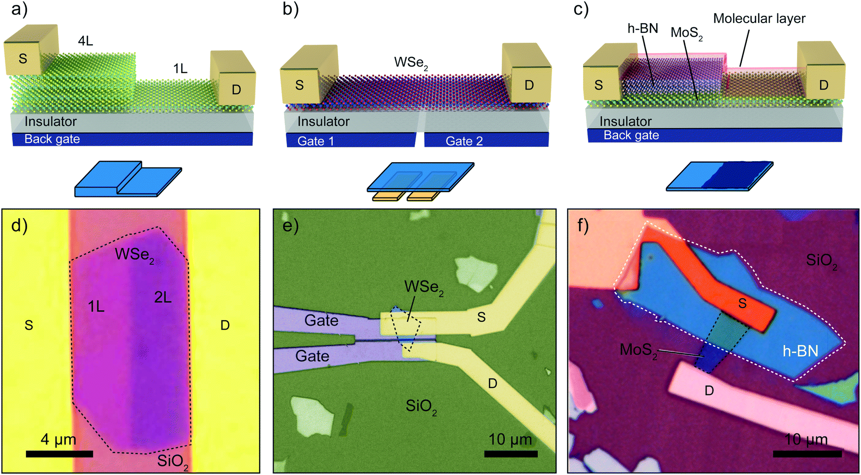 | ||
| Fig. 4 Different examples of p–n junctions based on 2D materials homojunctions. (a–c) Schematic diagram of a p–n junction based on (a) MoS2 with different thickness, (b) ambipolar WSe2 with two split gate electrodes and (c) local molecular doping of partially h-BN encapsulated MoS2. (d) Optical image of a thickness-modulated p–n junction based on single-layer and bilayer WSe2. (e) Optical image of a split-gate homojunction as schematically drawn in panel (b). (f) Optical image of a chemically doped MoS2 p–n junction as schematically illustrated in panel (c). The device is covered with molecules and part of the MoS2 is protected by a h-BN flake. Panel (d) readapted from ref. 73 with permission from IOP Publishing, panel (e) readapted from ref. 77 with permission from Springer Nature and panel (f) readapted from ref. 88 with permission from American Chemical Society (copyright 2014). | ||
3.2. Heterostructures
The combination of two different 2D materials to form a heterostructure is one of the most promising strategies because of the large variety of bandgap energies and doping types available among the different 2D materials. Fig. 5a and b show schematic diagrams of a vertical and a lateral heterojunction.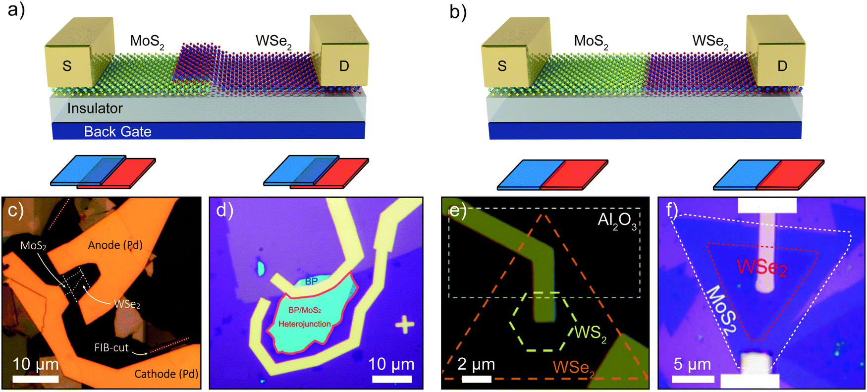 | ||
| Fig. 5 p–n junctions based on heterojunctions between two different 2D materials. (a and b) Schematic diagram of a vertical (a) and lateral (b) p–n junction. (c) Optical image of a vertical p–n junction formed by stacking a monolayer MoS2 flake onto a monolayer WSe2 flake. (d) Optical image of a vertical MoS2-black phosphorous device. The dark purple region is monolayer MoS2, while the blue flake is few-layer black phosphorus. The light purple region is SiO2. (e) Optical image of a lateral WSe2–WS2 p–n junction. The white dashed contour highlights an insulating Al2O3 layer, which allows for each electrode to contact only the WSe2 or WS2 respectively. (f) Optical image of a WSe2–MoS2 p–n junction device with different electrodes. Panel (c) readapted from ref. 111 with permission from American Chemical Society (copyright 2014), panel (d) readapted from ref. 113 with permission from American Chemical Society (copyright 2014), panel (e) readapted from ref. 70 with permission from Springer Nature and panel (f) readapted from ref. 114 with permission from The American Association for the Advancement of Science. | ||
The freedom of stacking 2D materials on top of each other permitted the fabrication of many different vertical stacks by this top-down approach. Among the different devices we find junctions between two TMDCs, such as WSe2–MoSe2 or MoTe2–MoS2, and junctions of a TMDC with a different 2D layered material, BP–MoS2, GaTe–MoS2 or with ultrathin membranes such as InAs–WSe2. Fig. 5d shows a BP–MoS2 vertical p–n junction113 fabricated by transferring a flake of few-layer BP onto a monolayer MoS2 grown by CVD onto a SiO2/Si substrate. More recently vertical p–n junctions were directly fabricated by epitaxial growth without the need of mechanical assembly.
3.3. Hybrid and mixed-dimensional
Apart from a purely 2D architecture, many efforts were dedicated to produce hybrid p–n junctions where a 2D material is in contact with a material of lower dimensionality, such as in the case of a molecular crystal or a nanotubes film, or higher dimensionality, like in the case of a bulk semiconductor such as Si. Fig. 6a and b show a schematic diagram of a 2D–0D and a 2D–3D p–n junction. | ||
| Fig. 6 p–n junctions produced by heterostructures with mixed dimensionality. (a and b) Schematic of mixed-dimensional 2D–0D (a) and 2D–3D (b) heterojunctions. (c) False colour SEM image of single wall carbon nanotubes (CNTs) single layer MoS2 p–n junction. (d) Optical image of a bilayer MoS2 flake on top of a SiO2/Si substrate to fabricate a 2D–0D heterojunction by depositing a CuPc molecular crystal through a shadow mask. (e) Optical image of a 2D–3D device in an intermediate state of fabrication. A monolayer MoS2 is placed across the sidewall of a square window etched into a SiO2 layer exposing the underlying p-doped silicon. Panel (c) readapted from ref. 115 with permission from National Academy of Sciences, panel (d) readapted from ref. 116 with permission from Royal Society of Chemistry and panel (e) readapted from ref. 117 with permission from American Chemical Society. | ||
Molecular organic crystals and nanotube films have surfaces with saturated bonds and are therefore free from dangling bonds. They typically interact via van der Waals forces and this allows the integration of these low-dimensional materials with 2D materials in van der Waals heterostructures.8,118Fig. 3c shows a colored scanning electron microscopy (SEM) image of a 1D–2D junction created by transferring a layer of sorted single-walled carbon nanotubes (SWCNTs) onto a single-layer MoS2 flake. A different kind of 1D–2D junctions have been demonstrated by joining a single nanowire and a 2D material. Among the works we find junctions between MoS2, WSe2 and BP and a ZnO nanowire.119–121Fig. 3d shows a microscope picture of a 0D–2D junction between a bilayer MoS2 flake and a 30 nm thick Cu-phthalocyanine (CuPC) thin film, thermally evaporated through a window opened in a PMMA layer.
Bulk materials such as Si or GaAs, which are largely used in conventional p–n junctions and electronics, can be used in conjunction with 2D materials to create novel p–n 2D–3D junctions. Lopez-Sanchez and coauthors117 realized a heterojunction composed of n-type monolayer MoS2 and p-type silicon. Fig. 6e shows this MoS2–Si device fabricated by transferring a MoS2 monolayer flake onto a prepatterned highly doped p-type Si substrate covered with SiO2 containing a window through which the underlying Si is exposed. Similar devices based on MoS2 and Si have been thoroughly studied in literature.122–124 A different geometry was shown by Wang et al.,125 who deposited vertically standing MoS2 onto a silicon substrate with a scalable sputtering method. Using different materials, Gehring et al.126 demonstrated a 2D–3D junction composed of a few tens of nanometer-thick black phosphorus flake on top of a highly n-doped GaAs substrate.
4. Electrical properties
4.1. The p–n junction as a rectifier
The first use of a p–n junction that we will discuss is that of a current rectifier. The built-in electric field at the p–n interface allows the flow of charge carriers in one direction (forward bias) while blocking the current in the other direction (backward bias). Many 2D based p–n junctions have been used as rectifiers, showing excellent performances and novel functionalities. One such example is the control of the rectification ratio with a gate field. Deng and coauthors reported gate-tunable rectifying current–voltage characteristics (IVs) in a monolayer MoS2–BP p–n junction (see Fig. 5d). Fig. 7a shows IVs recorded at various gate voltages between −30 V and 50 V. At negative gate voltages they observe a reduction of both the forward current (p-type connected to positive voltage and n-type to negative voltage) and of the reverse current (p-type connected to negative voltage and n-type to positive voltage). Increasing the gate voltage leads to an increase of both the forward and the reverse current in the device. The rectification ratio, defined as the ratio of the forward/reverse current, increases as the back gate voltage decreases as can be seen in Fig. 7b. At a gate voltage of −30 V, a rectification ratio of 105 is obtained. This modulation can be achieved because the band alignment between MoS2 and black phosphorus at the p–n junction interface can be tuned by the gate voltage. Moreover, the gate voltage also modulates the sheet resistance and the contact resistance of the MoS2 and BP respectively.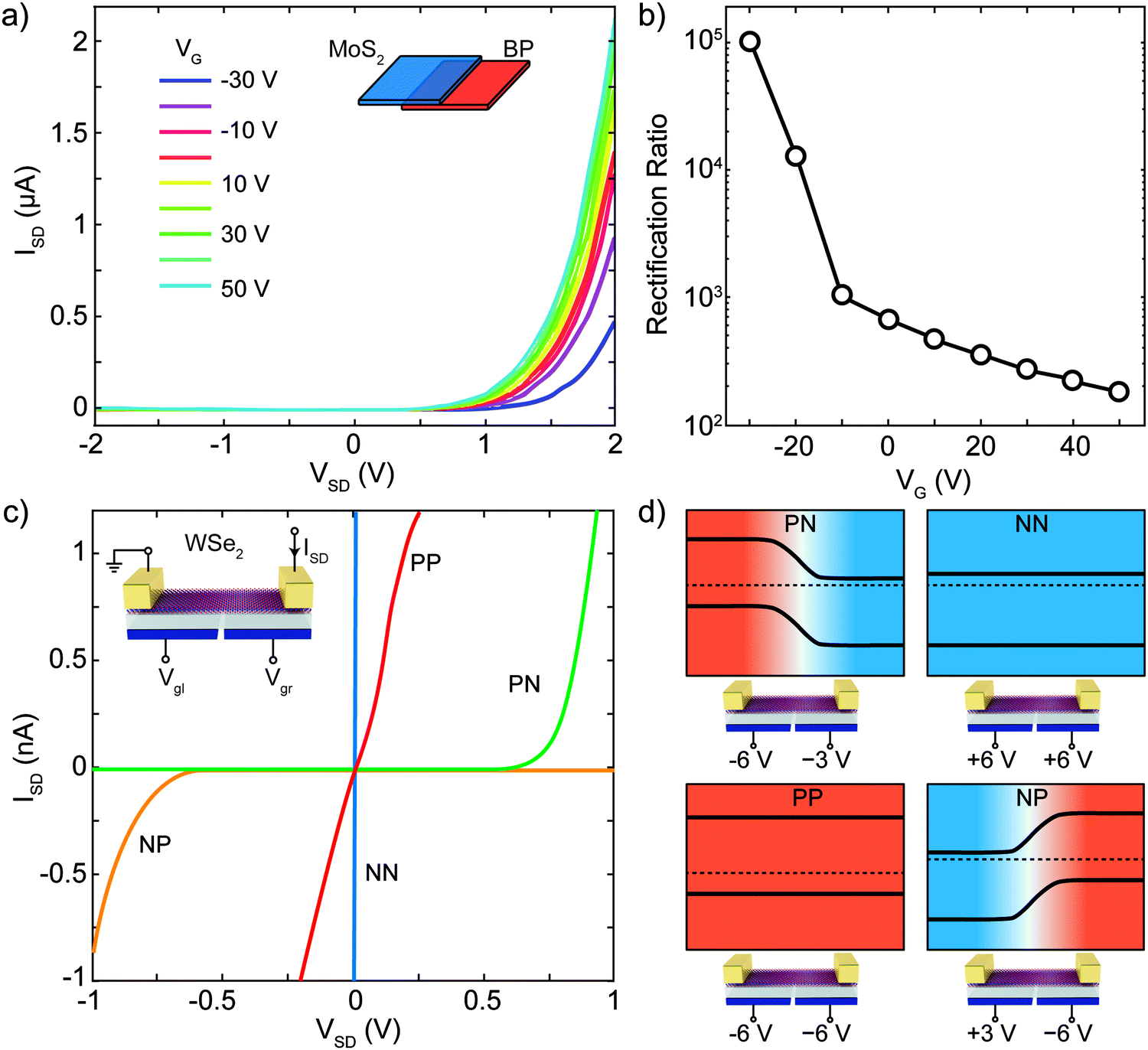 | ||
| Fig. 7 Atomically thin diodes based on 2D p–n junctions. (a) Gate tunable current–voltage (IV) characteristics of a BP–MoS2 vertical heterojunction. (b) Rectification ratio at VSD = ±2 V as a function of gate voltage of the device of panel (a). (c) IV characteristics of a double-gated WSe2 homojunction device in different local gate configurations. (d) Schematic diagram of the band structure and the state of the local gates of the device in panel (c) in PP, PN, NP and NN configuration. Panels (a) and (b) readapted from ref. 113 with permission from American Chemical Society (copyright 2014) and panel (c) readapted from ref. 79 with permission from American Chemical Society (copyright 2014). | ||
A second kind of devices, that can be called “reconfigurable diode”, employs electrostatic doped p–n junctions based on a split gate configuration, which allows inducing locally hole- and electron-doping in different parts of the channel; a new feature introduced by the 2D nature of the devices.76–78Fig. 7c shows for example the IV characteristics of a double-gated monolayer WSe2 homojunction studied by Groenendijk and coauthors.79 By tuning the Fermi energy both hole- and electron-doping can be readily accessed due to the ambipolarity of WSe2. Two of the four IVs of Fig. 7c are linear (NN and PP configuration) while the other two are highly non-linear (PN and NP configuration) displaying rectifying behavior, whose direction can be controlled by the gate bias polarity. The voltages applied to the local gates used to achieve these four configurations are shown in Fig. 7d together with a simplified band diagram of the device.
4.2. Physical mechanism of the electrical transport
Although the shape and features of the IV characteristics of 2D p–n junctions are similar to those of a conventional p–n junction, the underlying physical mechanism of rectification can be very different. When considering the two model junctions depicted in Fig. 8a one can see that reducing the thickness of the p- and n-type materials modifies the interface between the two materials. In a bulk p–n junction, charge transfer at the interface between the two materials creates a depletion region from which all the free charges are removed. In the case of atomically thin junctions (for example in a vertical junction between monolayer MoS2 and monolayer WSe2) such a depletion region cannot be formed because of the reduced thickness. Simplified diagrams of the band profiles for a multilayer and a monolayer junction, taken along the thickness direction, are shown in Fig. 8a. While the bands of the p- and n-type materials bend in the depletion region in the bulk case (right panels), a sharp discontinuity of the bands is present at the monolayer interface (left panels). | ||
| Fig. 8 p–n junctions in bulk and ultra-thin materials. (a) Schematic of the devices (top) and band profiles (bottom) in a multilayer-multilayer p–n junction (right) and monolayer–monolayer (left). In the bottom panels, energy is depicted on the vertical axis and the device thickness on the x-axis. (b) Schematic of the bands in a bulk p–n junction under equilibrium (VSD = 0 V) and under forward and reverse bias. (c and d) Schematic diagrams of interlayer recombination (c) in a monolayer–monolayer p–n junction and of (d) the exciton dissociation process. | ||
The depletion region in a bulk p–n junction is modified by the application of a voltage as schematically depicted in Fig. 8b. While under forward voltage the size of the depletion region is reduced, under reverse bias its size increases. With increasing forward voltage, the depletion zone eventually becomes thin enough that the built-in electric field cannot counteract charge carrier motion across the p–n junction; this leads to an increase in current. In the case of an atomically thin junction under forward bias the current is governed by tunneling-mediated interlayer recombination between majority carriers at the bottom (top) of the conduction (valence) band of the n-type (p-type) material. This interlayer recombination (Fig. 8c) can be described by two physical mechanisms or a combination of both: Langevin recombination, which is mediated by Coulomb interaction and describes the direct recombination of an electron and a hole, or Shockley–Read–Hall (SRH) recombination, which is mediated by inelastic tunnelling of majority carriers into trap states in the gap.127–130 These two processes can be present both at the same time in a 2D p–n junction and each of these processes predicts a different dependence of the electron–hole recombination ratio on the majority carriers density. The rectifying IVs characteristics can then be explained by an increase of the interlayer recombination rate under forward bias and the photocurrent generated in a 2D junction and its dependence on a gate field can be modeled by the two recombination processes.112
5. Optoelectronic properties
5.1. Response to illumination: photodetectors and solar cells
p–n junctions constitute the central building blocks of photodetectors, solar cells and light emitting diodes (LEDs). Their main application is thus in optoelectronics. Typically, there are two operating modes for p–n junctions: photovoltaic mode (PV), in which the p–n junction is not biased, and photoconductive mode (PC), where the p–n junction works under reverse external bias.131,132 The PV effect forms the basis for the solar cells. The PC mode is used in photodetection applications and has the advantages of having a lower capacitance that improves the response time and the presence of an external electric field facilitates the separation of electro–hole pairs improving the responsivity.Some of the most studied vertical p–n junctions are heterostructures made from WSe2 and MoS2.109,111,112 In the work by Furchi et al.111 the authors transferred a mechanically exfoliated monolayer of WSe2 on top of a monolayer MoS2, both on a SiO2/Si substrate, with source and drain electrodes placed in contact with each of the materials. Due to the ambipolar nature of WSe2, this device could be tuned into n–n junction or p–n junction regimes by means of the back gate voltage and, in the p–n configuration, a rectification ratio of ∼100 was achieved. By illuminating the device in the p–n configuration with a white light source, a photovoltaic effect was observed, as shown in the IVs of Fig. 9a measured at increasing optical powers, with an external quantum efficiency (EQE) of ∼1.5% and a power conversion efficiency of ∼0.2%. In this vertical p–n junction, photons are absorbed in both materials generating electron–hole pairs followed by relaxation of the photogenerated carriers and charge transfer between the layers (see Fig. 8c and d). The carriers have to laterally diffuse to the electrodes and electron–hole recombination may occur reducing the efficiency of the solar cell. Lee et al.112 circumvented this issue by employing graphene electrodes, sandwiching the semiconducting monolayers, and enhancing the responsivity of the devices by a factor of ∼5. This increase in responsivity comes mainly from the smaller travel distance that the photoexcited carriers have to travel to reach the electrodes leading to a more efficient carrier extraction in the vertical direction as shown in Fig. 9b. In order to increase the EQE of the devices, solar cells involving materials with different thicknesses were investigated, finding EQEs of 2.4%, 12% and 34% for monolayer, bilayer and multilayer p–n junctions respectively. This improvement is due not only to the enhanced light absorption in the multilayer devices, but also due to the exponential suppression of direct electron tunnelling between the two graphene electrodes. In an optimized (∼15 nm thick) MoS2–WSe2 multilayer heterostructure, Wong et al.133 demonstrated internal photocarrier collection efficiencies exceeding 70% and power conversion efficiencies of up to 3.4% at 633 nm wavelength.
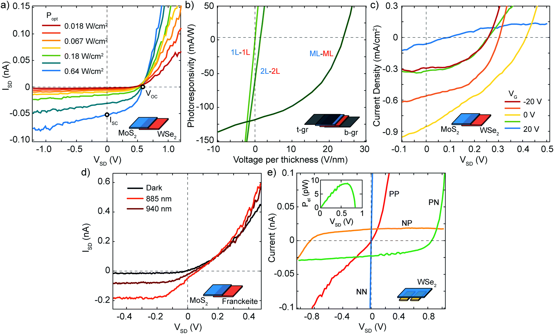 | ||
| Fig. 9 Optoelectronic properties of 2D p–n junctions. (a) Current–voltage (IV) characteristics of a WSe2–MoS2 vertical heterojunction at different illumination powers. (b) Photoresponsivity versus voltage traces of WSe2–MoS2 vertical heterojunctions sandwiched between two graphene electrodes for three devices with different thickness of the WSe2 and MoS2 flakes. The x-axis of each trace is normalized by the thickness of the corresponding heterojunction. (c) Gate tunable IV characteristics of a WSe2–MoS2 vertical heterojunction kept under illumination. (d) IV characteristics of a franckeite–MoS2 vertical heterojunction in dark and under infrared illumination. (e) IV characteristics of a double-gated WSe2 device under optical illumination. The biasing conditions are: PN (Vgl = −40 V, Vgr = 40 V), NP (Vgl = 40 V, Vgr = −40 V), NN (Vgl = Vgr = 40 V), PP (Vgl = Vgr = −40 V). When operated as a diode (PN and NP), electrical power (Pel) can be extracted. Inset: Pelversus voltage in the PN configuration. Panel (a) readapted from ref. 111 with permission from American Chemical Society, panels (b) and (c) readapted from ref. 112 with permission from Springer Nature, panel (d) readapted from ref. 135, panel (e) readapted from ref. 77 with permission from Springer Nature. | ||
Furthermore, other combinations of p- and n-doped materials have been explored to realize vertical solar cells, although p-doped 2D materials are less frequent than n-doped materials. Among the naturally p-doped 2D semiconductors we list black phosphorus, franckeite and MoTe2. Deng et al. investigated a BP–MoS2 vertical p–n heterojunction working in the visible range of the electromagnetic spectrum with a peak EQE of 0.3%,113 a value lower than that of WSe2–MoS2 solar cells. Nevertheless, one of the most attractive features of BP is its low bandgap, allowing light absorption also in the near-infrared part of the electromagnetic spectrum. MoS2–BP junctions have shown EQEs up to ∼20% under illumination with 1.55 μm wavelength light, employing few-layer flakes of both BP and MoS2.134 More recently, Molina-Mendoza et al. investigated the capability of franckeite as near-infrared solar cell in a p–n junction formed by multilayer franckeite-monolayer MoS2 able to generate an electrical power of ∼1 pW under infrared illumination with wavelength of 940 nm as shown in Fig. 9d.135 Also, few-layer MoTe2-few-layer MoS2136 and monolayer MoTe2–MoS2137 p–n junctions have shown promising results in light detection and energy harvesting in the near-infrared. The junction between monolayer MoTe2–MoS2 shows photoresponse at 1550 nm, due to interlayer transitions between the two materials.137 However, for the individual device made of a pure MoS2 or MoTe2 monolayer, no photoresponse is observed at 1550 nm.
Lateral 2D junctions are also very promising for optoelectronic applications. In the case of heterojunctions, several combinations of materials have already been achieved and studied as energy harvesting devices. CVD grown WSe2–MoS2 was used by Li et al. to build a p–n junction which showed an open-circuit voltage of 220 meV under white light illumination.114 In another work, the authors found for the same system (Fig. 9d) a power conversion efficiency of 2.6% and an increased open-circuit voltage of 390 meV.138 Devices based on laterally grown MoSe2–MoS2 and WS2–WSe2 heterostructures have also been studied by Duan et al., where the authors found that the WS2–WSe2 heterostructures show rectifying behaviour and a photovoltaic effect, yielding an open-circuit voltage of 470 meV and an EQE of ∼10%.70
With respect to homostructures, the most studied materials are WSe2 and BP due to their ambipolar nature that allows for electrostatic doping of different region of the semiconductor channel. Three different groups independently reported a solar cell built by inducing p and n doping in a single-layer WSe2 flake by means of local back-gate electrodes (see Fig. 4b).76–78Fig. 9e shows IVs of this device under illumination in different configurations of the local gates. The IVs shows that photogeneration in PV mode occurs only in the NP and PN configurations, with clear short-circuit current and open-circuit voltage. The inset of Fig. 9e shows the photovoltaic power that can be extracted in the PN configuration. Baugher et al. and Pospischil et al. reported an external quantum efficiency for their solar cells of 0.2% and 0.5%, respectively. Alternatively, Buscema et al. reported a similar device structure employing BP as the semiconductor channel,80 which permitted to extend the range of power generation for wavelengths up to 940 nm. On the other hand, the WSe2 devices are limited to the visible region of the electromagnetic spectrum.
5.2. Scanning photocurrent studies
The experiments discussed above were performed under global illumination, that is by illuminating the device with a spot larger than its size. We will now turn to local illumination and specifically to scanning photocurrent (SPC) studies. By scanning a diffraction-limited light spot over a device while measuring the current one can construct SPC maps that yield information on the spatial profile of the bands or the electric fields present in the device.139–144 This information is crucial to understand the underlying mechanisms ruling the photocurrent generation. The ultrathin nature of 2D p–n junctions allows the light to easily reach the p–n interface both in lateral and in vertical architectures.64,78,145,146Fig. 10a shows an optical image of a vertical p–n junction composed of elemental doped p-MoS2 and n-MoS2.64 By recording a SPC map at zero bias the authors studied the local generation of the short circuit current in the device arising from the PV effect. Fig. 10b shows such a map recorded with a laser of 532 nm and with highlighted contours of the n- and p-type flakes. A negative photocurrent (blue/red regions) is generated in the region where the two MoS2 flakes overlap as a result of the strong electric field in the depletion region that separates the photocarriers. Compared to global illumination, the SPC map highlights that photocurrent generation can be non-homogeneous across the overlapping region. In Fig. 10b, a hotspot is clearly present, indicating that the interaction between the two flakes is not spatially homogenous, most likely due to the presence of interlayer adsorbates trapped between the layers during the assembly of the device. | ||
| Fig. 10 Scanning photocurrent studies of 2D p–n junctions. (a) Optical image of the device. (b) Photocurrent image of the MoS2 p–n junction from panel (a) with zero bias voltage applied (map of the short circuit current). (c) Microscope image of a monolayer WSe2 electrostatic p–n junction device. The source and drain contacts are white and the two bottom gates are red. (d) Corresponding scanning photocurrent image showing pronounced photocurrent generation localized at the junction. The black dashed lines outline the back gates whereas the white dashed line present the WSe2 flake. (e) Integrated photoluminescence map. (f) Photoluminescence peak energy map showing p and n regions as a result of the different energies of oppositely charged excitons. X− (X+) represents the negatively (positively) charged exciton found in the n (p) region. Panels (a) and (b) readapted from ref. 64 with permission from John Wiley and Sons and panels (c), (d), (e) and (f) readapted from ref. 78 with permission from Springer Nature. | ||
SPC studies have also been conducted in lateral devices such as the one depicted in Fig. 10c. Ross et al. combined SPC maps with photoluminescence (PL) maps to study an electrostatically gated WSe2 device.78 The zero bias SPC map, shown in Fig. 10d, has been recorded at 100 K with a 660 nm laser and shows that the photocurrent generation occurs at the interface between the p- and the n-doped regions. Fig. 10e presents the corresponding map of the integrated PL intensity, which is homogenous across the whole WSe2 flake, indicating that the luminescence is not quenched by the underlying gates. More revealingly, Fig. 10f shows a color map of the peak photoluminescence photon energy, exhibiting two distinct regions clearly correlated with the n-doped (blue) and p-doped (red) regions of the WSe2 flake. Above the gate held at Vgl = +8.0 V the presence of negatively charged X− trions (two electrons and one hole) dominates, while above the other gate, held at Vgr = −8.0 V, the higher-energy positively charged X+ trions (two holes and one electron) are more frequent, implying an excess of holes.
5.3. Electroluminescence: light emitting diodes
Electroluminescence is the result of radiative recombination of electrons and holes in a material, usually a semiconductor, which release their energy as photons. The most basic requirement for efficient light emission is a direct optical transition in the semiconductor, as in the case of monolayer semiconducting TMDCs. Electrically driven light emission produced by a unipolar current in single layer MoS2 FETs has been reported to take place near the contact electrodes via impact excitation147 or in a suspended sheet by Joule heating.148 However, effective emission requires the injection of both electrons and holes, which is typically achieved using a p–n junction.LEDs based on 2D materials have been realized in different ways, employing different materials and device architectures. For example, the ambipolar nature of single layer WSe2 has been exploited to generate light by employing local gates to electrostatically dope different regions in a semiconductor channel, forming a lateral p–n junction device.76–78 This kind of device (Fig. 4a and d) exhibited electroluminescence efficiencies (ratio between emitted optical power and electrical input power) ranging between 0.1 and 1%, with energy emission peaks at 752 nm (see Fig. 11a, ref. 77) and 751 nm (Fig. 11b, ref. 76) at room temperature. The difference between the energy of the emission peaks is attributed to different dielectric environments that can influence the exciton binding energy.
 | ||
| Fig. 11 Light emission from 2D p–n junctions. (a) Electroluminescence (EL) emission spectra of a monolayer WSe2 electrostatic p–n junction recorded for constant currents of 50, 100 and 200 nA. The curves are offset for clarity. The green curve demonstrates that no light emission is obtained under unipolar (n-type) conduction. (b) Left axis: External quantum efficiency (EQE) as a function of wavelength at a constant laser power of 2 mW in a monolayer WSe2 device. Peaks in the EQE correspond to exciton transitions A, B and A′, as labelled. Right axis: Electroluminescence intensity from a monolayer WSe2 electrostatic p–n junction. The traces are offset vertically for clarity. Inset: Diagram of the band structure around the K and Q points, with arrows indicating the lowest-energy exciton transitions for monolayer WSe2. (c) Circularly polarized EL spectrum of a WSe2 electric double-layer transistor for different voltages. Inset: Diagram of the band structure around the K and K′ points. (d) Intensity map showing the electroluminescent emission of a MoS2/Si hybrid p–n junction. The entire surface of the heterojunction is emitting light. (e) False color EL image of a MoS2–WSe2 heterojunction device under an injection current of 100 μA. (f) EL spectra of a monolayer WSe2/MoS2 heterojunction at different injection current. Panel (a) readapted from ref. 77 with permission from Springer Nature, panel (b) readapted from ref. 76 with permission from Springer Nature, panel (c) readapted from ref. 149 with permission from The American Association for the Advancement of Science, panel (d) readapted from ref. 117 with permission from American Chemical Society, and panels (e) and (f) readapted from ref. 154 with permission from American Chemical Society. | ||
Zhang et al. have employed mono- and few-layer WSe2 in p-i-n (i, intrinsic) junctions with an electric double-layer transistor (EDLT) architecture,149 where the doping of the semiconductor channel is modified by tuning the voltage between the drain and source electrodes with respect to the gate electrode, enabling the accumulation of opposite charge carriers close to each of the electrodes. This device configuration circumvents the requirement of using monolayers for light emission due to the breakdown of the inversion symmetry in few-layer flakes under high-gate fields, and it also enables the emission of circularly polarized light as shown in Fig. 11c. A similar device structure has been used to induce light emission by means of liquid-gated transistors employing mono- and bilayer WS2,150 CVD-MoS2151 or bulk ReS2.152
Concerning electroluminescent heterojunctions and mixed dimensional junctions many examples have been reported in literature. Lopez-Sanchez et al. demonstrated the light emission from a monolayer MoS2-highly p-doped Si hybrid junction (see Fig. 6e).117Fig. 11d shows a gray-scale optical picture of the electroluminescence generated from the device, which exhibits peak emission at ∼2 eV. This emission energy is blue-shifted by almost 200 meV from the monolayer MoS2 exciton energy, which is due to the influence of the dielectric environment. The authors also reported that devices with unencapsulated MoS2 show a significant reduction of current and emitted light intensity after a few days in ambient conditions. On the other hand, by encapsulating the MoS2 monolayer with 30 nm thick HfO2 or Al2O3 the stability of the device can be greatly extended. In a different study Li et al. reported EL from a p-i-n junction between multilayer MoS2 and a GaN substrate, using Al2O3 as insulator.153
Furthermore, LEDs based on 2D heterostructures have been reported. Cheng et al. measured the light emission from a WSe2/MoS2 vertical heterojunction.154 In this case, both monolayer-WSe2/few-layer-MoS2 and bilayer-WSe2/few-layer-MoS2 were investigated (Fig. 11e), revealing different features in the emission spectrum related to excitonic peaks A (Fig. 11f) and B (not shown here), hot electron luminescence peaks A′ and B′ (Fig. 11f) and indirect bandgap emission (not shown here). Table 2 lists some photonic properties of electroluminescent 2D p–n junctions.
| Materials p/n | Peak emission (nm) | Threshold current (nA) | Notes | Ref. |
|---|---|---|---|---|
| WSe2 | 752 | 4 | — | 77 |
| WSe2 | 751 | 50 | Estimated electroluminescence efficiency ηEL ≈ 0.1% | 76 |
| WSe2 | 750 | 5 | — | 78 |
| WSe2 | 740 | 1000 | Emission of circularly polarized light | 149 |
| Si/MoS2 | 620 | 109 | Stable after encapsulation with 30 nm thick oxide | 117 |
| WSe2/MoS2 | 792 | 150![[thin space (1/6-em)]](https://www.rsc.org/images/entities/char_2009.gif) 000 000 |
— | 154 |
| WS2 | 630 | — | — | 150 |
| MoS2 | 650 | 40000 |
Large-area MoS2 monolayer grown by chemical vapor deposition | 151 |
6. Comparison between devices
In this section we show three tables that list the different p–n junctions based on 2D materials found in literature. Table 3 contains the 2D homojunctions, Table 4 the 2D heterojunctions and Table 5 the mixed-dimensional junctions. For each device we report some of the relevant parameters such as the materials composing the device and the thickness. We also list figure of merits for electronic or optoelectronic applications such as the rectification ratio, the responsivity or the open circuit voltage. In the “Materials” column, in the case of heterojunctions and mixed-dimensional junctions the two materials used are listed with the p-type as first and the n-type as second material. In the “Thickness” column the thickness of the junction is given either in nm or in number of layers (indicated by the code nL where n is the number of layers, ML stays for multilayer).| Homojunctions | Materials p/n | Thickness (nm) | Rectification ratio | V OC (V) | Ref. |
|---|---|---|---|---|---|
| Thickness | WSe2 | 2L/1L | 10 | — | 73 |
| MoS2 | ML/1L | 1000 | 0 | 74 | |
| MoSe2 | 4/28 | 100000 |
0.24 | 155 | |
| BP | 11L/6L | 600 | 0.21 | 156 | |
| Electrostatic | WSe2 | 5.0 | 10000 |
0.83 | 83 |
| WSe2 | 1L | 50 | 0.03 | 78 | |
| WSe2 | 1L | 500 | 0.85 | 77 | |
| WSe2 | 1L | 100000 |
0.72 | 76 | |
| BP | 6.5 | 11 | 0.05 | 80 | |
| WSe2 | 1L | — | 0.7 | 79 | |
| Chemical | MoS2 | 3 | 100 | 0.6 | 99 |
| MoS2 | 60 | 100 | 0.5 | 88 | |
| MoS2 | 7 | 10 | — | 88 | |
| BP | 3 | 100000 |
0.45 | 98 | |
| BP | 10 | 50 | — | 97 | |
| Elemental | MoSe2 | 6 | 1000000 |
0.35 | 157 |
| MoS2 | 15 | — | 0.45 | 103 | |
| BP | 8.5 | 5600 | 0.14 | 158 | |
| MoS2 | 10 | 250 | 0.58 | 64 | |
| Heterojunctions | Materials p/n | Thickness (nm) | Rectification ratio | V OC (V) | Ref. |
|---|---|---|---|---|---|
| Vertical | WSe2/MoS2 | 1L/1L | 50 | 0.55 | 111 |
| WSe2/MoS2 | 1L/1L | 50 | 0.5 | 112 | |
| WSe2/MoS2 | 2L/13L | 15 | 0.27 | 154 | |
| BP/MoS2 | 11/1L | 100000 |
0.3 | 113 | |
| WSe2/MoS2 | 5/10 | 50 | 0.28 | 159 | |
| WSe2/MoSe2 | 1L/1L | 50 | 0.055 | 160 | |
| WS2/MoS2 | ML/ML | 10000 |
0.25 | 161 | |
| GaTe/MoS2 | 20 | 400000 |
0.22 | 162 | |
| InAs/WSe2 | >20 | 1000000 |
— | 163 | |
| BP/MoS2 | 15 | >100 | 0.36 | 164 | |
| MoTe2/MoS2 | 1L/1L | 10 | 0.15 | 137 | |
| MoTe2/MoS2 | 4L/4L | 4000 | 0.3 | 136 | |
| WSe2/MoSe2 | 3L/3L | 10000 |
0.46 | 165 | |
| WSe2/BP | 12/20 | 2500 | 0.29 | 166 | |
| Franckeite/MoS2 | 25/1.4 | 400 | 0.08 | 135 | |
| ReSe2/MoS2 | 60/7 | 60000 |
0.1 | 167 | |
| ReS2/ReSe2 | 64/48 | 3150 | 0.18 | 168 | |
| GaSe/InSe | 19/13 | 200000 |
— | 169 | |
| GeSe/MoS2 | — | >100 | — | 170 | |
| WSe2/MoS2 | 9 | 1000 | — | 171 | |
| MoTe2/SnSe2 | 31 | 1000 | — | 171 | |
| SnSe/MoS2 | 28/7 | 100000 |
— | 172 | |
| SnS/WS2 | 200/0.7 | 15 | — | 173 | |
| WSe2/SnS2 | 1L/1L | 10000000 |
0.03 | 174 | |
| CuO/MoS2 | 150/1L | 10 | — | 175 | |
| Lateral | WS2/MoS2 | 1L | 100 | 0.12 | 65 |
| WSe2/WS2 | ML | — | 0.47 | 70 | |
| In2Se3/CuInSe2 | 14 | 10 | 0.03 | 72 | |
| WSe2/MoS2 | 1L | 10 | 0.22 | 114 | |
| Heterojunctions | Materials p/n | Thickness (nm) | Rectification ratio | V OC (V) | Ref. |
|---|---|---|---|---|---|
| 2D–0D, 2D–1D | SWCNT/MOS2 | —/1L | 10000 |
— | 115 |
| Rubrene/MoS2 | 300/5 | 100000 |
— | 176 | |
| Pentacene/MoS2 | 40/2L | 5 | 0.3 | 177 | |
| C8-BTBT/MoS2 | 5 | 100000 |
0.5 | 178 | |
| CuPC/MoS2 | 20/1L | 10000 |
0.6 | 116 | |
| 2D–3D | Si/MoS2 | 1L | — | 0.41 | 122 |
| Ge/MoS2 | 2L | 2 | — | 179 | |
| Si/MoS2 | 1L | 100 | 0.58 | 117 | |
| BP/GaAs | 15 | 120 | 0.55 | 126 | |
| WS2/GaN | 400 | 1000 | — | 180 | |
| Si/MoS2 | 12.5 | 20 | — | 181 | |
| Si/Bi2Se3 | — | 50 | 0.24 | 182 | |
| LSMO/MoS2 | 1L | 1000 | 0.4 | 183 | |
7. Future perspective and challenges
Despite the large number of experiments discussed in this Review, many challenges still need to be overcome for the integration of 2D p–n junctions in mass-produced electronic components. The two most important challenges are the large-scale fabrication of 2D p–n junctions and the environmental degradation of 2D materials.7.1. Large-scale fabrication and environmental degradation
The first main challenge is related to the large-scale production of tailored van der Waals heterostructures with well-controlled interfaces. Even if the deterministic placement methods are very successful for laboratory-scale experiments, they are not suited for commercial applications. Growing methods like the CVD growth described in Section 2.2.2 have already proven to be capable of growing high-quality 2D materials including lateral and vertical heterostructures at a laboratory-scale. van der Waals epitaxial methods hold even more promises to the synthesis of high-quality 2D heterostructures. Up-scaling of these growth methods is possible and in the years to come the realization of higher quality devices can be expected.184 A second, promising strategy to up-scale the production of 2D p–n junctions is to combine the growth of single 2D materials (such as MoS2) with various doping techniques (mostly chemical or electrostatic).A second challenge is the environmental degradation of many of the known 2D materials. For example, when exposed to air, black phosphorous in its ultrathin form tends to uptake moisture which degrades the electronic properties of the material.37–40 In the case of BP the most accepted mechanism for the degradation involves the reaction of the material with oxygen which changes the material properties.185,186 One way to prevent this degradation is by encapsulating the air-sensitive material between two flakes of h-BN under oxygen- and moisture-free conditions.187–189 One active area of 2D materials research is therefore dedicated to up-scale the encapsulation methods. A different approach that is currently pursued is the active search for new 2D materials, which do not present degradation problems, that could come either from synthesis (for example TiS3) or from natural sources (e.g. franckeite).46,135,190,191 This active search already helped to increase the number of available 2D materials from just a handful to more than twenty in less than ten years.
7.2. Future perspectives
Apart from conventional optoelectronic applications, 2D p–n junctions hold still many unexplored applications and fundamental questions. For example, thermoelectric applications of 2D p–n junctions have not been thoroughly investigated yet. The traditional Peltier device, a component largely used in electronics for cooling (and less commonly for heating), is based on a p-type and a n-type semiconductor thermally connected in parallel and electrically in series. van der Waals heterostructures could be used to fabricate atomically thin cooling (or heating) elements combined with the other attractive properties of 2D materials, such as the high transparence or the flexibility. Another interesting route is the study of novel p–n junction geometries (like for example circular p–n junctions recently demonstrated in graphene192,193) or new devices based on 2D p–n junctions, such as memories or logic gates.83,194The real possibilities still hidden in 2D materials are probably many more than the ones discussed and 2D p–n junctions hold many promises for commercial applications. These 2D junctions are especially interesting building blocks for flexible and transparent electronic components, such as solar cells or light emitting diodes.195,196 Another application that can benefit from the ultrathin nature of 2D p–n junctions is in light sensing and harvesting applications or for nanophotonics.14,197 As we discussed in Section 5, 2D p–n junctions can be used as photodetectors and many materials combinations are available that can be used to design devices sensible to wavelengths ranging from the infrared to the ultraviolet have already been demonstrated.134,135,137
8. Conclusions
In recent years we have witnessed the production of novel p–n junctions that take advantage of the ultrathin nature of 2D materials. Both bottom-up and top-down production methods have proven capable of creating p–n junctions of high quality with exquisite optoelectronic properties. In this Review we have revised the recent progress on 2D p–n junctions, discussing the most used materials and fabrication methods and examples of 2D p–n junctions from literature belonging to eight different junction architectures. With these architectures different applications have been realized and we have discussed experiments that use 2D p–n junctions respectively as rectifiers, as photodetectors/solar cells and as light emitting diodes. Finally a comparison between the important figures of merit of the various devices from literature is made. By no means, this field is closed. 2D materials continue to offer many opportunities to fabricate novel p–n junctions with outstanding properties that open up exciting scientific routes both in terms of fundamental questions and in term of applications.Conflicts of interest
The authors declare no competing financial interests.Acknowledgements
AC-G acknowledges funding from the European Commission under the Graphene Flagship, contract CNECTICT-604391. RF acknowledges support from the Netherlands Organization for Scientific Research (NWO) through the research program Rubicon with project number 680-50-1515. This project further received funding from the European Union's Horizon 2020 research and innovation program under grant agreement No. 696656 (Graphene Flagship).References
- M. Riordan and L. Hoddeson, IEEE Spectrum, 1997, 34, 46–51 CrossRef.
- Q. H. Wang, K. Kalantar-Zadeh, A. Kis, J. N. Coleman and M. S. Strano, Nat. Nanotechnol., 2012, 7, 699–712 CrossRef CAS PubMed.
- S. J. Kim, K. Choi, B. Lee, Y. Kim and B. H. Hong, Annu. Rev. Mater. Res., 2015, 45, 63–84 CrossRef CAS.
- H. Schmidt, F. Giustiniano and G. Eda, Chem. Soc. Rev., 2015, 44, 7715–7736 RSC.
- S. Das, J. A. Robinson, M. Dubey, H. Terrones and M. Terrones, Annu. Rev. Mater. Res., 2015, 45, 1–27 CrossRef CAS.
- K. Novoselov, A. Mishchenko, A. Carvalho and A. C. Neto, Science, 2016, 353, aac9439 CrossRef CAS PubMed.
- Y. Liu, N. O. Weiss, X. Duan, H.-C. Cheng, Y. Huang and X. Duan, Nat. Rev. Mater., 2016, 1, 16042 CrossRef CAS.
- D. Jariwala, T. J. Marks and M. C. Hersam, Nat. Mater., 2016, 16, 170–181 CrossRef PubMed.
- K. S. Novoselov, A. K. Geim, S. V. Morozov, D. Jiang, Y. Zhang, S. V. Dubonos, I. V. Grigorieva and A. A. Firsov, Science, 2004, 306, 666–669 CrossRef CAS PubMed.
- V. Nicolosi, M. Chhowalla, M. G. Kanatzidis, M. S. Strano and J. N. Coleman, Science, 2013, 340, 1226419 CrossRef.
- K. Novoselov, D. Jiang, F. Schedin, T. Booth, V. Khotkevich, S. Morozov and A. Geim, Proc. Natl. Acad. Sci. U. S. A., 2005, 102, 10451–10453 CrossRef CAS PubMed.
- K. Novoselov and A. C. Neto, Phys. Scr., 2012, 2012, 014006 CrossRef.
- P. Miró, M. Audiffred and T. Heine, Chem. Soc. Rev., 2014, 43, 6537–6554 RSC.
- A. Castellanos-Gomez, Nat. Photonics, 2016, 10, 202–204 CrossRef CAS.
- R. Roldan, L. Chirolli, E. Prada, J. A. Silva-Guillen, P. San-Jose and F. Guinea, Chem. Soc. Rev., 2017, 46, 4387–4399 RSC.
- B. Partoens and F. Peeters, Phys. Rev. B: Condens. Matter Mater. Phys., 2006, 74, 075404 CrossRef.
- M. Y. Han, B. Özyilmaz, Y. Zhang and P. Kim, Phys. Rev. Lett., 2007, 98, 206805 CrossRef PubMed.
- K. F. Mak, C. H. Lui, J. Shan and T. F. Heinz, Phys. Rev. Lett., 2009, 102, 256405 CrossRef PubMed.
- D. C. Elias, R. R. Nair, T. Mohiuddin, S. Morozov, P. Blake, M. Halsall, A. Ferrari, D. Boukhvalov, M. Katsnelson and A. Geim, Science, 2009, 323, 610–613 CrossRef CAS PubMed.
- F. Xia, D. B. Farmer, Y.-m. Lin and P. Avouris, Nano Lett., 2010, 10, 715–718 CrossRef CAS PubMed.
- R. Balog, B. Jørgensen, L. Nilsson, M. Andersen, E. Rienks, M. Bianchi, M. Fanetti, E. Lægsgaard, A. Baraldi and S. Lizzit, Nat. Mater., 2010, 9, 315–319 CrossRef CAS PubMed.
- Y. Lin and J. W. Connell, Nanoscale, 2012, 4, 6908–6939 RSC.
- M. Chhowalla, H. S. Shin, G. Eda, L.-J. Li, K. P. Loh and H. Zhang, Nat. Chem., 2013, 5, 263 CrossRef PubMed.
- D. Jariwala, V. K. Sangwan, L. J. Lauhon, T. J. Marks and M. C. Hersam, ACS Nano, 2014, 8, 1102–1120 CrossRef CAS PubMed.
- X. Duan, C. Wang, A. Pan, R. Yu and X. Duan, Chem. Soc. Rev., 2015, 44, 8859–8876 RSC.
- O. V. Yazyev and A. Kis, Mater. Today, 2015, 18, 20–30 CrossRef CAS.
- W. Choi, N. Choudhary, G. H. Han, J. Park, D. Akinwande and Y. H. Lee, Mater. Today, 2017, 20, 116–130 CrossRef CAS.
- S. Manzeli, D. Ovchinnikov, D. Pasquier, O. V. Yazyev and A. Kis, Nat. Rev. Mater., 2017, 2, 17033 CrossRef CAS.
- H. Li, J. Wu, Z. Yin and H. Zhang, Acc. Chem. Res., 2014, 47, 1067–1075 CrossRef CAS PubMed.
- K. F. Mak, C. Lee, J. Hone, J. Shan and T. F. Heinz, Phys. Rev. Lett., 2010, 105, 136805 CrossRef PubMed.
- A. Splendiani, L. Sun, Y. Zhang, T. Li, J. Kim, C.-Y. Chim, G. Galli and F. Wang, Nano Lett., 2010, 10, 1271–1275 CrossRef CAS PubMed.
- B. Radisavljevic, A. Radenovic, J. Brivio, V. Giacometti and A. Kis, Nat. Nanotechnol., 2011, 6, 147–150 CrossRef CAS PubMed.
- F. Xia, H. Wang and Y. Jia, Nat. Commun., 2014, 5, 4458 CAS.
- J. Yang, R. Xu, J. Pei, Y. W. Myint, F. Wang, Z. Wang, S. Zhang, Z. Yu and Y. Lu, Light: Sci. Appl., 2015, 4, e312 CrossRef CAS.
- R. Gusmao, Z. Sofer and M. Pumera, Angew. Chem., 2017, 56, 8052–8072 CrossRef CAS PubMed.
- A. Castellanos-Gomez, L. Vicarelli, E. Prada, J. O. Island, K. Narasimha-Acharya, S. I. Blanter, D. J. Groenendijk, M. Buscema, G. A. Steele and J. Alvarez, 2D Mater., 2014, 1, 025001 CrossRef.
- J. O. Island, G. A. Steele, H. S. van der Zant and A. Castellanos-Gomez, 2D Mater., 2015, 2, 011002 CrossRef.
- J. D. Wood, S. A. Wells, D. Jariwala, K.-S. Chen, E. Cho, V. K. Sangwan, X. Liu, L. J. Lauhon, T. J. Marks and M. C. Hersam, Nano Lett., 2014, 14, 6964–6970 CrossRef CAS PubMed.
- J.-S. Kim, Y. Liu, W. Zhu, S. Kim, D. Wu, L. Tao, A. Dodabalapur, K. Lai and D. Akinwande, Sci. Rep., 2015, 5, 8989 CrossRef CAS PubMed.
- A. Favron, E. Gaufrès, F. Fossard, A.-L. Phaneuf-L’Heureux, N. Y. Tang, P. L. Lévesque, A. Loiseau, R. Leonelli, S. Francoeur and R. Martel, Nat. Mater., 2015, 14, 826–832 CrossRef CAS PubMed.
- A. Molle, J. Goldberger, M. Houssa, Y. Xu, S.-C. Zhang and D. Akinwande, Nat. Mater., 2017, 16, 163–169 CrossRef CAS PubMed.
- S. Balendhran, S. Walia, H. Nili, S. Sriram and M. Bhaskaran, Small, 2015, 11, 640–652 CrossRef CAS PubMed.
- L.-D. Zhao, S.-H. Lo, Y. Zhang, H. Sun, G. Tan, C. Uher, C. Wolverton, V. P. Dravid and M. G. Kanatzidis, Nature, 2014, 508, 373–377 CrossRef CAS PubMed.
- C. W. Li, J. Hong, A. F. May, D. Bansal, S. Chi, T. Hong, G. Ehlers and O. Delaire, Nat. Phys., 2015, 11, 1063–1069 CrossRef CAS.
- S. Srivastava and B. Avasthi, J. Mater. Sci., 1992, 27, 3693–3705 CrossRef CAS.
- J. O. Island, A. J. Molina-Mendoza, M. Barawi, R. Biele, E. Flores, J. M. Clamagirand, J. R. Ares, C. Sánchez, H. S. van der Zant and R. D’Agosta, 2D Mater., 2017, 4, 022003 CrossRef.
- B. Huang, G. Clark, E. Navarro-Moratalla, D. R. Klein, R. Cheng, K. L. Seyler, D. Zhong, E. Schmidgall, M. A. McGuire, D. H. Cobden, W. Yao, D. Xiao, P. Jarillo-Herrero and X. Xu, Nature, 2017, 546, 270–273 CrossRef CAS PubMed.
- M. A. McGuire, Crystals, 2017, 7, 121 CrossRef.
- M. Osada and T. Sasaki, J. Mater. Chem., 2009, 19, 2503–2511 RSC.
- R. Ma and T. Sasaki, Acc. Chem. Res., 2014, 48, 136–143 CrossRef PubMed.
- B. Anasori, M. R. Lukatskaya and Y. Gogotsi, Nat. Rev. Mater., 2017, 2, 16098 CrossRef CAS.
- J. Kang, S. Tongay, J. Zhou, J. Li and J. Wu, Appl. Phys. Lett., 2013, 102, 012111 CrossRef.
- Y. Liu, P. Stradins and S.-H. Wei, Sci. Adv., 2016, 2, e1600069 Search PubMed.
- V. Tran, R. Soklaski, Y. Liang and L. Yang, Phys. Rev. B: Condens. Matter Mater. Phys., 2014, 89, 235319 CrossRef.
- Y. Cai, G. Zhang and Y.-W. Zhang, Sci. Rep., 2014, 4, 6677 CrossRef CAS PubMed.
- P. Blake, E. Hill, A. Castro Neto, K. Novoselov, D. Jiang, R. Yang, T. Booth and A. Geim, Appl. Phys. Lett., 2007, 91, 063124 CrossRef.
- Z. Ni, H. Wang, J. Kasim, H. Fan, T. Yu, Y. Wu, Y. Feng and Z. Shen, Nano Lett., 2007, 7, 2758–2763 CrossRef CAS PubMed.
- S. Roddaro, P. Pingue, V. Piazza, V. Pellegrini and F. Beltram, Nano Lett., 2007, 7, 2707–2710 CrossRef CAS PubMed.
- R. Frisenda, E. Navarro-Moratalla, P. Gant, D. P. De Lara, P. Jarillo-Herrero, R. V. Gorbachev and A. Castellanos-Gomez, Chem. Soc. Rev., 2018, 47, 53–68 RSC.
- C. R. Dean, A. F. Young, I. Meric, C. Lee, L. Wang, S. Sorgenfrei, K. Watanabe, T. Taniguchi, P. Kim and K. L. Shepard, Nat. Nanotechnol., 2010, 5, 722–726 CrossRef CAS PubMed.
- P. Zomer, S. Dash, N. Tombros and B. Van Wees, Appl. Phys. Lett., 2011, 99, 232104 CrossRef.
- A. Castellanos-Gomez, M. Buscema, R. Molenaar, V. Singh, L. Janssen, H. S. van der Zant and G. A. Steele, 2D Mater., 2014, 1, 011002 CrossRef.
- L. Wang, I. Meric, P. Huang, Q. Gao, Y. Gao, H. Tran, T. Taniguchi, K. Watanabe, L. Campos and D. Muller, Science, 2013, 342, 614–617 CrossRef CAS PubMed.
- C. Reuter, R. Frisenda, D. Y. Lin, T. S. Ko, D. Perez de Lara and A. Castellanos-Gomez, Small Methods, 2017, 1, 1700119 CrossRef.
- Y. Gong, J. Lin, X. Wang, G. Shi, S. Lei, Z. Lin, X. Zou, G. Ye, R. Vajtai and B. I. Yakobson, Nat. Mater., 2014, 13, 1135–1142 CrossRef CAS PubMed.
- J. Yu, J. Li, W. Zhang and H. Chang, Chem. Sci., 2015, 6, 6705–6716 RSC.
- S. L. Wong, H. Liu and D. Chi, Prog. Cryst. Growth Charact. Mater., 2016, 62, 9–28 CrossRef CAS.
- R. Dong and I. Kuljanishvili, J. Vac. Sci. Technol., B: Nanotechnol. Microelectron.: Mater., Process., Meas., Phenom., 2017, 35, 030803 Search PubMed.
- Y. Cui, B. Li, J. Li and Z. Wei, Sci. China: Phys., Mech. Astron., 2018, 61, 016801 CrossRef.
- X. Duan, C. Wang, J. C. Shaw, R. Cheng, Y. Chen, H. Li, X. Wu, Y. Tang, Q. Zhang and A. Pan, Nat. Nanotechnol., 2014, 9, 1024–1030 CrossRef CAS PubMed.
- C. Huang, S. Wu, A. M. Sanchez, J. J. Peters, R. Beanland, J. S. Ross, P. Rivera, W. Yao, D. H. Cobden and X. Xu, Nat. Mater., 2014, 13, 1096–1101 CrossRef CAS PubMed.
- Z. Zheng, J. Yao and G. Yang, ACS Appl. Mater. Interfaces, 2017, 9, 7288–7296 CAS.
- Z.-Q. Xu, Y. Zhang, Z. Wang, Y. Shen, W. Huang, X. Xia, W. Yu, Y. Xue, L. Sun and C. Zheng, 2D Mater., 2016, 3, 041001 CrossRef.
- M. Sun, D. Xie, Y. Sun, W. Li, C. Teng and J. Xu, Sci. Rep., 2017, 7, 4505 CrossRef PubMed.
- R. Bratschitsch, Nat. Nanotechnol., 2014, 9, 247–248 CrossRef CAS PubMed.
- B. W. Baugher, H. O. Churchill, Y. Yang and P. Jarillo-Herrero, Nat. Nanotechnol., 2014, 9, 262–267 CrossRef CAS PubMed.
- A. Pospischil, M. M. Furchi and T. Mueller, Nat. Nanotechnol., 2014, 9, 257–261 CrossRef CAS PubMed.
- J. S. Ross, P. Klement, A. M. Jones, N. J. Ghimire, J. Yan, D. Mandrus, T. Taniguchi, K. Watanabe, K. Kitamura and W. Yao, Nat. Nanotechnol., 2014, 9, 268–272 CrossRef CAS PubMed.
- D. J. Groenendijk, M. Buscema, G. A. Steele, S. Michaelis de Vasconcellos, R. Bratschitsch, H. S. van der Zant and A. Castellanos-Gomez, Nano Lett., 2014, 14, 5846–5852 CrossRef CAS PubMed.
- M. Buscema, D. J. Groenendijk, G. A. Steele, H. S. J. van der Zant and A. Castellanos-Gomez, Nat. Commun., 2014, 5, 4651 CrossRef CAS PubMed.
- N. M. Gabor, J. C. Song, Q. Ma, N. L. Nair, T. Taychatanapat, K. Watanabe, T. Taniguchi, L. S. Levitov and P. Jarillo-Herrero, Science, 2011, 334, 648–652 CrossRef CAS PubMed.
- H.-Y. Chiu, V. Perebeinos, Y.-M. Lin and P. Avouris, Nano Lett., 2010, 10, 4634–4639 CrossRef CAS PubMed.
- D. Li, M. Chen, Z. Sun, P. Yu, Z. Liu, P. M. Ajayan and Z. Zhang, Nat. Nanotechnol., 2017, 12, 901–906 CrossRef CAS PubMed.
- J. Ye, S. Inoue, K. Kobayashi, Y. Kasahara, H. Yuan, H. Shimotani and Y. Iwasa, Nat. Mater., 2010, 9, 125–128 CrossRef CAS PubMed.
- Y. Zhang, J. Ye, Y. Matsuhashi and Y. Iwasa, Nano Lett., 2012, 12, 1136–1140 CrossRef CAS PubMed.
- Y. Zhang, J. Ye, Y. Yomogida, T. Takenobu and Y. Iwasa, Nano Lett., 2013, 13, 3023–3028 CrossRef CAS PubMed.
- A. A. El Yumin, J. Yang, Q. Chen, O. Zheliuk and J. Ye, Phys. Status Solidi B, 2017, 254, 1700180 CrossRef.
- M. S. Choi, D. Qu, D. Lee, X. Liu, K. Watanabe, T. Taniguchi and W. J. Yoo, ACS Nano, 2014, 8, 9332–9340 CrossRef CAS PubMed.
- S. Mouri, Y. Miyauchi and K. Matsuda, Nano Lett., 2013, 13, 5944–5948 CrossRef CAS PubMed.
- J. D. Lin, C. Han, F. Wang, R. Wang, D. Xiang, S. Qin, X. A. Zhang, L. Wang, H. Zhang, A. T. Wee and W. Chen, ACS Nano, 2014, 8, 5323–5329 CrossRef CAS PubMed.
- C. R. Ryder, J. D. Wood, S. A. Wells, Y. Yang, D. Jariwala, T. J. Marks, G. C. Schatz and M. C. Hersam, Nat. Chem., 2016, 8, 597–602 CrossRef CAS PubMed.
- G. Abellán, V. Lloret, U. Mundloch, M. Marcia, C. Neiss, A. Görling, M. Varela, F. Hauke and A. Hirsch, Angew. Chem., Int. Ed., 2016, 55, 14557–14562 CrossRef PubMed.
- A. J. Molina-Mendoza, L. Vaquero-Garzon, S. Leret, L. de Juan-Fernández, E. M. Pérez and A. Castellanos-Gomez, Chem. Commun., 2016, 52, 14365–14368 RSC.
- X. He, W. Chow, F. Liu, B. Tay and Z. Liu, Small, 2017, 13, 1602558 CrossRef PubMed.
- E. C. Peters, E. J. Lee, M. Burghard and K. Kern, Appl. Phys. Lett., 2010, 97, 193102 CrossRef.
- D. B. Farmer, Y.-M. Lin, A. Afzali-Ardakani and P. Avouris, Appl. Phys. Lett., 2009, 94, 213106 CrossRef.
- X. Yu, S. Zhang, H. Zeng and Q. J. Wang, Nano Energy, 2016, 25, 34–41 CrossRef CAS.
- G. Wang, L. Bao, T. Pei, R. Ma, Y.-Y. Zhang, L. Sun, G. Zhang, H. Yang, J. Li and C. Gu, Nano Lett., 2016, 16, 6870–6878 CrossRef CAS PubMed.
- H.-M. Li, D. Lee, D. Qu, X. Liu, J. Ryu, A. Seabaugh and W. J. Yoo, Nat. Commun., 2015, 6, 6564 CrossRef CAS PubMed.
- J. Legma, G. Vacquier, H. Traore and A. Casalot, Mater. Sci. Eng., B, 1991, 8, 167–174 CrossRef.
- J. Suh, T. E. Park, D. Y. Lin, D. Fu, J. Park, H. J. Jung, Y. Chen, C. Ko, C. Jang, Y. Sun, R. Sinclair, J. Chang, S. Tongay and J. Wu, Nano Lett., 2014, 14, 6976–6982 CrossRef CAS PubMed.
- Y. Jin, D. H. Keum, S. J. An, J. Kim, H. S. Lee and Y. H. Lee, Adv. Mater., 2015, 27, 5534–5540 CrossRef CAS PubMed.
- S. A. Svatek, E. Antolín, D.-Y. Lin, R. Frisenda, C. Reuter, A. J. Molina-Mendoza, M. Muñoz, N. Agrait, T.-S. Ko, D. P. de Lara and A. Castellanos-Gomez, J. Mater. Chem. C, 2017, 5, 854–861 RSC.
- A. Nipane, D. Karmakar, N. Kaushik, S. Karande and S. Lodha, ACS Nano, 2016, 10, 2128–2137 CrossRef CAS PubMed.
- E. Kim, C. Ko, K. Kim, Y. Chen, J. Suh, S. G. Ryu, K. Wu, X. Meng, A. Suslu and S. Tongay, Adv. Mater., 2016, 28, 341–346 CrossRef CAS PubMed.
- A. K. Geim and I. V. Grigorieva, Nature, 2013, 499, 419–425 CrossRef CAS PubMed.
- M.-Y. Li, C.-H. Chen, Y. Shi and L.-J. Li, Mater. Today, 2016, 19, 322–335 CrossRef CAS.
- A. Pant, Z. Mutlu, D. Wickramaratne, H. Cai, R. K. Lake, C. Ozkan and S. Tongay, Nanoscale, 2016, 8, 3870–3887 RSC.
- H. Fang, C. Battaglia, C. Carraro, S. Nemsak, B. Ozdol, J. S. Kang, H. A. Bechtel, S. B. Desai, F. Kronast and A. A. Unal, Proc. Natl. Acad. Sci. U. S. A., 2014, 111, 6198–6202 CrossRef CAS PubMed.
- X. Hong, J. Kim, S.-F. Shi, Y. Zhang, C. Jin, Y. Sun, S. Tongay, J. Wu, Y. Zhang and F. Wang, Nat. Nanotechnol., 2014, 9, 682–686 CrossRef CAS PubMed.
- M. M. Furchi, A. Pospischil, F. Libisch, J. Burgdörfer and T. Mueller, Nano Lett., 2014, 14, 4785–4791 CrossRef CAS PubMed.
- C. H. Lee, G. H. Lee, A. M. van der Zande, W. Chen, Y. Li, M. Han, X. Cui, G. Arefe, C. Nuckolls, T. F. Heinz, J. Guo, J. Hone and P. Kim, Nat. Nanotechnol., 2014, 9, 676–681 CrossRef CAS PubMed.
- Y. Deng, Z. Luo, N. J. Conrad, H. Liu, Y. Gong, S. Najmaei, P. M. Ajayan, J. Lou, X. Xu and P. D. Ye, ACS Nano, 2014, 8, 8292–8299 CrossRef CAS PubMed.
- M.-Y. Li, Y. Shi, C.-C. Cheng, L.-S. Lu, Y.-C. Lin, H.-L. Tang, M.-L. Tsai, C.-W. Chu, K.-H. Wei and J.-H. He, Science, 2015, 349, 524–528 CrossRef CAS PubMed.
- D. Jariwala, V. K. Sangwan, C.-C. Wu, P. L. Prabhumirashi, M. L. Geier, T. J. Marks, L. J. Lauhon and M. C. Hersam, Proc. Natl. Acad. Sci. U. S. A., 2013, 110, 18076–18080 CrossRef CAS PubMed.
- S. Vélez, J. Island, M. Buscema, O. Txoperena, S. Parui, G. A. Steele, F. Casanova, H. S. van der Zant, A. Castellanos-Gomez and L. E. Hueso, Nanoscale, 2015, 7, 15442–15449 RSC.
- O. Lopez-Sanchez, E. Alarcon Llado, V. Koman, A. Fontcuberta i Morral, A. Radenovic and A. Kis, ACS Nano, 2014, 8, 3042–3048 CrossRef CAS PubMed.
- H. Huang, Y. Huang, S. Wang, M. Zhu, H. Xie, L. Zhang, X. Zheng, Q. Xie, D. Niu and Y. Gao, Crystals, 2016, 6, 113 CrossRef.
- S. H. H. Shokouh, A. Pezeshki, A. Raza, S. Raza, H. S. Lee, S. W. Min, P. J. Jeon, J. M. Shin and S. Im, Adv. Mater., 2015, 27, 150–156 CrossRef CAS PubMed.
- P. J. Jeon, Y. T. Lee, J. Y. Lim, J. S. Kim, D. K. Hwang and S. Im, Nano Lett., 2016, 16, 1293–1298 CrossRef CAS PubMed.
- S. H. Hosseini Shokouh, A. Pezeshki, S. R. A. Raza, K. Choi, S.-W. Min, P. J. Jeon, H. S. Lee and S. Im, ACS Nano, 2014, 8, 5174–5181 CrossRef CAS PubMed.
- M.-L. Tsai, S.-H. Su, J.-K. Chang, D.-S. Tsai, C.-H. Chen, C.-I. Wu, L.-J. Li, L.-J. Chen and J.-H. He, ACS Nano, 2014, 8, 8317–8322 CrossRef CAS PubMed.
- L. Hao, Y. Liu, W. Gao, Z. Han, Q. Xue, H. Zeng, Z. Wu, J. Zhu and W. Zhang, J. Appl. Phys., 2015, 117, 114502 CrossRef.
- V. Dhyani and S. Das, Sci. Rep., 2017, 7, 44243 CrossRef PubMed.
- L. Wang, J. Jie, Z. Shao, Q. Zhang, X. Zhang, Y. Wang, Z. Sun and S. T. Lee, Adv. Funct. Mater., 2015, 25, 2910–2919 CrossRef CAS.
- P. Gehring, R. Urcuyo, D. L. Duong, M. Burghard and K. Kern, Appl. Phys. Lett., 2015, 106, 233110 CrossRef.
- P. Langevin, Ann. Chim. Phys., 1903, 28, 122 Search PubMed.
- W. Shockley and W. Read Jr, Phys. Rev., 1952, 87, 835 CrossRef CAS.
- R. N. Hall, Phys. Rev., 1952, 87, 387 CrossRef CAS.
- N. Greenham and P. Bobbert, Phys. Rev. B: Condens. Matter Mater. Phys., 2003, 68, 245301 CrossRef.
- M. M. Furchi, D. K. Polyushkin, A. Pospischil and T. Mueller, Nano Lett., 2014, 14, 6165–6170 CrossRef CAS PubMed.
- J. O. Island, S. I. Blanter, M. Buscema, H. S. J. van der Zant and A. Castellanos-Gomez, Nano Lett., 2015, 15, 7853–7858 CrossRef CAS PubMed.
- J. Wong, D. Jariwala, G. Tagliabue, K. Tat, A. R. Davoyan, M. C. Sherrott and H. A. Atwater, ACS Nano, 2017, 11, 7230–7240 CrossRef CAS PubMed.
- L. Ye, H. Li, Z. Chen and J. Xu, ACS Photonics, 2016, 3, 692–699 CrossRef CAS.
- A. J. Molina-Mendoza, E. Giovanelli, W. S. Paz, M. A. Niño, J. O. Island, C. Evangeli, L. Aballe, M. Foerster, H. S. Van Der Zant, G. Rubio-Bollinger, N. Agraït, J. J. Palacios, E. M. Pérez and A. Castellanos-Gomez, Nat. Commun., 2017, 8, 14409 CrossRef CAS PubMed.
- A. Pezeshki, S. H. H. Shokouh, T. Nazari, K. Oh and S. Im, Adv. Mater., 2016, 28, 3216–3222 CrossRef CAS PubMed.
- K. Zhang, T. Zhang, G. Cheng, T. Li, S. Wang, W. Wei, X. Zhou, W. Yu, Y. Sun and P. Wang, ACS Nano, 2016, 10, 3852–3858 CrossRef CAS PubMed.
- M. L. Tsai, M. Y. Li, J. R. D. Retamal, K. T. Lam, Y. C. Lin, K. Suenaga, L. J. Chen, G. Liang, L. J. Li and H. He Jr, Adv. Mater., 2017, 29, 1701168 CrossRef PubMed.
- Y. Ahn, A. Tsen, B. Kim, Y. W. Park and J. Park, Nano Lett., 2007, 7, 3320–3323 CrossRef CAS PubMed.
- F. Xia, T. Mueller, R. Golizadeh-Mojarad, M. Freitag, Y.-m. Lin, J. Tsang, V. Perebeinos and P. Avouris, Nano Lett., 2009, 9, 1039–1044 CrossRef CAS PubMed.
- H. Yuan, X. Liu, F. Afshinmanesh, W. Li, G. Xu, J. Sun, B. Lian, A. G. Curto, G. Ye and Y. Hikita, Nat. Nanotechnol., 2015, 10, 707–713 CrossRef CAS PubMed.
- G. Rao, M. Freitag, H.-Y. Chiu, R. S. Sundaram and P. Avouris, ACS Nano, 2011, 5, 5848–5854 CrossRef CAS PubMed.
- M. Tosun, D. Fu, S. B. Desai, C. Ko, J. S. Kang, D.-H. Lien, M. Najmzadeh, S. Tongay, J. Wu and A. Javey, Sci. Rep., 2015, 5, 10990 CrossRef PubMed.
- S. Kallatt, G. Umesh, N. Bhat and K. Majumdar, Nanoscale, 2016, 8, 15213–15222 RSC.
- M. C. Lemme, F. H. Koppens, A. L. Falk, M. S. Rudner, H. Park, L. S. Levitov and C. M. Marcus, Nano Lett., 2011, 11, 4134–4137 CrossRef CAS PubMed.
- S. L. Howell, D. Jariwala, C.-C. Wu, K.-S. Chen, V. K. Sangwan, J. Kang, T. J. Marks, M. C. Hersam and L. J. Lauhon, Nano Lett., 2015, 15, 2278–2284 CrossRef CAS PubMed.
- R. Sundaram, M. Engel, A. Lombardo, R. Krupke, A. Ferrari, P. Avouris and M. Steiner, Nano Lett., 2013, 13, 1416–1421 CrossRef CAS PubMed.
- L. Dobusch, S. Schuler, V. Perebeinos and T. Mueller, Adv. Mater., 2017, 29, 1701304 CrossRef PubMed.
- Y. Zhang, T. Oka, R. Suzuki, J. Ye and Y. Iwasa, Science, 2014, 344, 725–728 CrossRef CAS PubMed.
- S. Jo, N. Ubrig, H. Berger, A. B. Kuzmenko and A. F. Morpurgo, Nano Lett., 2014, 14, 2019–2025 CrossRef CAS PubMed.
- E. Ponomarev, I. Gutiérrez-Lezama, N. Ubrig and A. F. Morpurgo, Nano Lett., 2015, 15, 8289–8294 CrossRef CAS PubMed.
- I. Gutiérrez-Lezama, B. A. Reddy, N. Ubrig and A. F. Morpurgo, 2D Mater., 2016, 3, 045016 CrossRef.
- D. Li, R. Cheng, H. Zhou, C. Wang, A. Yin, Y. Chen, N. O. Weiss, Y. Huang and X. Duan, Nat. Commun., 2015, 6, 7509 CrossRef PubMed.
- R. Cheng, D. Li, H. Zhou, C. Wang, A. Yin, S. Jiang, Y. Liu, Y. Chen, Y. Huang and X. Duan, Nano Lett., 2014, 14, 5590–5597 CrossRef CAS PubMed.
- Y. Yang, N. Huo and J. Li, J. Mater. Chem. C, 2017, 5, 7051–7056 RSC.
- L. Wang, L. Huang, W. C. Tan, X. Feng, L. Chen and K.-W. Ang, Adv. Electron. Mater., 2018, 4, 1700442 CrossRef.
- Y. Jin, D. H. Keum, S. J. An, J. Kim, H. S. Lee and Y. H. Lee, Adv. Mater., 2015, 27, 5534–5540 CrossRef CAS PubMed.
- Y. Liu, Y. Cai, G. Zhang, Y. W. Zhang and K. W. Ang, Adv. Funct. Mater., 2017, 27, 1604368 Search PubMed.
- J. Ahn, P. J. Jeon, S. R. A. Raza, A. Pezeshki, S.-W. Min, D. K. Hwang and S. Im, 2D Mater., 2016, 3, 045011 CrossRef.
- Y. Gong, S. Lei, G. Ye, B. Li, Y. He, K. Keyshar, X. Zhang, Q. Wang, J. Lou and Z. Liu, Nano Lett., 2015, 15, 6135–6141 CrossRef CAS PubMed.
- N. Huo, J. Kang, Z. Wei, S. S. Li, J. Li and S. H. Wei, Adv. Funct. Mater., 2014, 24, 7025–7031 CrossRef CAS.
- F. Wang, Z. Wang, K. Xu, F. Wang, Q. Wang, Y. Huang, L. Yin and J. He, Nano Lett., 2015, 15, 7558–7566 CrossRef CAS PubMed.
- S. Chuang, R. Kapadia, H. Fang, T. Chia Chang, W.-C. Yen, Y.-L. Chueh and A. Javey, Appl. Phys. Lett., 2013, 102, 242101 CrossRef.
- T. Hong, B. Chamlagain, T. Wang, H.-J. Chuang, Z. Zhou and Y.-Q. Xu, Nanoscale, 2015, 7, 18537–18541 RSC.
- N. Flöry, A. Jain, P. Bharadwaj, M. Parzefall, T. Taniguchi, K. Watanabe and L. Novotny, Appl. Phys. Lett., 2015, 107, 123106 CrossRef.
- P. Chen, T. T. Zhang, J. Xiang, H. Yu, S. Wu, X. Lu, G. Wang, F. Wen, Z. Liu and R. Yang, Nanoscale, 2016, 8, 3254–3258 RSC.
- X. Wang, L. Huang, Y. Peng, N. Huo, K. Wu, C. Xia, Z. Wei, S. Tongay and J. Li, Nano Res., 2016, 9, 507–516 CrossRef CAS.
- A.-J. Cho, S. D. Namgung, H. Kim and J.-Y. Kwon, APL Mater., 2017, 5, 076101 CrossRef.
- F. Yan, L. Zhao, A. Patanè, P. a. Hu, X. Wei, D. Zhang, Q. Lv, Q. Feng, C. Shen and K. Chang, Nanotechnology, 2017, 28, 27LT01 CrossRef PubMed.
- W. C. Yap, Z. Yang, M. Mehboudi, J.-A. Yan, S. Barraza-Lopez and W. Zhu, Nano Res., 2017, 11, 420–430 CrossRef.
- C. Li, X. Yan, X. Song, W. Bao, S. Ding, D. W. Zhang and P. Zhou, Nanotechnology, 2017, 28, 415201 CrossRef PubMed.
- S. Yang, M. Wu, B. Wang, L.-D. Zhao, L. Huang, C. Jiang and S.-H. Wei, ACS Appl. Mater. Interfaces, 2017, 9, 42149–42155 CAS.
- A. S. Aji, M. Izumoto, K. Suenaga, K. Yamamoto, H. Nakashima and H. Ago, Phys. Chem. Chem. Phys., 2018, 20, 889–897 RSC.
- T. Yang, B. Zheng, Z. Wang, T. Xu, C. Pan, J. Zou, X. Zhang, Z. Qi, H. Liu and Y. Feng, Nat. Commun., 2017, 8, 1906 CrossRef PubMed.
- K. Zhang, M. Peng, W. Wu, J. Guo, G. Gao, Y. Liu, J. Kou, R. Wen, Y. Lei and A. Yu, Mater. Horiz., 2017, 4, 274–280 RSC.
- F. Liu, W. L. Chow, X. He, P. Hu, S. Zheng, X. Wang, J. Zhou, Q. Fu, W. Fu and P. Yu, Adv. Funct. Mater., 2015, 25, 5865–5871 CrossRef CAS.
- D. Jariwala, S. L. Howell, K.-S. Chen, J. Kang, V. K. Sangwan, S. A. Filippone, R. Turrisi, T. J. Marks, L. J. Lauhon and M. C. Hersam, Nano Lett., 2015, 16, 497–503 CrossRef PubMed.
- D. He, Y. Pan, H. Nan, S. Gu, Z. Yang, B. Wu, X. Luo, B. Xu, Y. Zhang and Y. Li, Appl. Phys. Lett., 2015, 107, 183103 CrossRef.
- D. Sarkar, X. Xie, W. Liu, W. Cao, J. Kang, Y. Gong, S. Kraemer, P. M. Ajayan and K. Banerjee, Nature, 2015, 526, 91–95 CrossRef CAS PubMed.
- Y. Yu, P. W. Fong, S. Wang and C. Surya, Sci. Rep., 2016, 6, 37833 CrossRef CAS PubMed.
- C. Yim, M. O'brien, N. McEvoy, S. Riazimehr, H. Schäfer-Eberwein, A. Bablich, R. Pawar, G. Iannaccone, C. Downing and G. Fiori, Sci. Rep., 2014, 4, 5458 CrossRef CAS PubMed.
- Z. Wang, M. Li, L. Yang, Z. Zhang and X. P. Gao, Nano Res., 2017, 10, 1872–1879 CrossRef CAS.
- Y. Niu, R. Frisenda, S. A. Svatek, G. Orfila, F. Gallego, P. Gant, N. Agraït, C. Leon, A. Rivera-Calzada and D. P. De Lara, 2D Mater., 2017, 4, 034002 CrossRef.
- K. Kang, S. Xie, L. Huang, Y. Han, P. Y. Huang, K. F. Mak, C.-J. Kim, D. Muller and J. Park, Nature, 2015, 520, 656 CrossRef CAS PubMed.
- Y. Huang, J. Qiao, K. He, S. Bliznakov, E. Sutter, X. Chen, D. Luo, F. Meng, D. Su and J. Decker, Chem. Mater., 2016, 28, 8330–8339 CrossRef CAS.
- F. Alsaffar, S. Alodan, A. Alrasheed, A. Alhussain, N. Alrubaiq, A. Abbas and M. R. Amer, Sci. Rep., 2017, 7, 44540 CrossRef CAS PubMed.
- R. A. Doganov, E. C. O’Farrell, S. P. Koenig, Y. Yeo, A. Ziletti, A. Carvalho, D. K. Campbell, D. F. Coker, K. Watanabe and T. Taniguchi, Nat. Commun., 2015, 6, 6647 CrossRef CAS PubMed.
- A. Avsar, I. J. Vera-Marun, J. Y. Tan, K. Watanabe, T. Taniguchi, A. H. Castro Neto and B. Ozyilmaz, ACS Nano, 2015, 9, 4138–4145 CrossRef CAS PubMed.
- Y. Cao, A. Mishchenko, G. Yu, E. Khestanova, A. Rooney, E. Prestat, A. Kretinin, P. Blake, M. Shalom and C. Woods, Nano Lett., 2015, 15, 4914–4921 CrossRef CAS PubMed.
- M. Velický, P. S. Toth, A. M. Rakowski, A. P. Rooney, A. Kozikov, C. R. Woods, A. Mishchenko, L. Fumagalli, J. Yin and V. Zólyomi, Nat. Commun., 2017, 8, 14410 CrossRef PubMed.
- G. Prando, Nat. Nanotechnol., 2017, 12, 191 CrossRef CAS PubMed.
- Y. Jiang, J. Mao, D. Moldovan, M. R. Masir, G. Li, K. Watanabe, T. Taniguchi, F. M. Peeters and E. Y. Andrei, Nat. Nanotechnol., 2017, 12, 1045 CrossRef CAS PubMed.
- R. Heinisch, F. Bronold and H. Fehske, Phys. Rev. B: Condens. Matter Mater. Phys., 2013, 87, 155409 CrossRef.
- M. Huang, S. Li, Z. Zhang, X. Xiong, X. Li and Y. Wu, Nat. Nanotechnol., 2017, 12, 1148–1154 CrossRef CAS PubMed.
- D. Akinwande, N. Petrone and J. Hone, Nat. Commun., 2014, 5, 5678 CrossRef CAS PubMed.
- G. Fiori, F. Bonaccorso, G. Iannaccone, T. Palacios, D. Neumaier, A. Seabaugh, S. K. Banerjee and L. Colombo, Nat. Nanotechnol., 2014, 9, 768–779 CrossRef CAS PubMed.
- F. Xia, H. Wang, D. Xiao, M. Dubey and A. Ramasubramaniam, Nat. Photonics, 2014, 8, 899 CrossRef CAS.
| This journal is © The Royal Society of Chemistry 2018 |