
 Open Access Article
 This Open Access Article is licensed under a Creative Commons Attribution-Non Commercial 3.0 Unported Licence
Lithium insertion into silicon electrodes studied by cyclic voltammetry and operando neutron reflectometry†
B.
Jerliu
 *a,
E.
Hüger
a,
L.
Dörrer
a,
B. K.
Seidlhofer
b,
R.
Steitz
b,
M.
Horisberger
c and
H.
Schmidt
ad
*a,
E.
Hüger
a,
L.
Dörrer
a,
B. K.
Seidlhofer
b,
R.
Steitz
b,
M.
Horisberger
c and
H.
Schmidt
ad
aTechnische Universität Clausthal, Institut für Metallurgie, AG Mikrokinetik, Robert-Koch-Str. 42, 38678 Clausthal-Zellerfeld, Germany. E-mail: bujar.jerliu@tu-clausthal.de
bHelmholtz-Zentrum Berlin für Materialien und Energie, Soft Matter and Functional Materials, Hahn-Meitner-Platz 1, Berlin, 14109, Germany
cLaboratory for Scientific Developments and Novel Materials, Paul-Scherrer-Institut, 5232 Villigen, Switzerland
dClausthaler Zentrum für Materialtechnik, Leibnizstraße 9, 38678 Clausthal-Zellerfeld, Germany
First published on 22nd August 2018
Abstract
Operando neutron reflectometry measurements were carried out to study the insertion of lithium into amorphous silicon film electrodes during cyclic voltammetry (CV) experiments at a scan rate of 0.01 mV s−1. The experiments allow mapping of regions where significant amounts of Li are incorporated/released from the electrode and correlation of the results to modifications of characteristic peaks in the CV curve. High volume changes up to 390% accompanied by corresponding modifications of the neutron scattering length density (which is a measure of the average Li fraction present in the electrode) are observed during electrochemical cycling for potentials below 0.3 V (lithiation) and above 0.2 V (delithiation), leading to a hysteretic behaviour. This is attributed to result from mechanical stress as suggested in the literature. Formation and modification of a surface layer associated with the solid electrolyte interphase (SEI) were observed during cycling. Within the first lithiation cycle the SEI grows to 120 Å for potentials below 0.5 V. Afterwards a reversible and stable modification of the SEI between 70 Å (delithiated state) and 120 Å (lithiated state) takes place.
1. Introduction
The enormous scientific and technological advancement in the field of renewable energy, portable electronic devices and electric vehicles during the last decades has strongly encouraged the development of new energy storage devices, such as Li-ion batteries.1,2 Li-ion battery technology can cover the needs of future energy storage like longer lifespan, and higher energy density and power density. This depends basically on the exploration of advanced materials to be present in Li-ion batteries.3 Today, lithium-ion batteries are broadly in use as rechargeable power sources for portable electronics and have increasing importance in the automotive sector. The Li-ion battery storage technology has also the potential to become important for the off-grid renewable energy sector.4 For these applications further improvements in energy density, driving range, battery weight, power density, cycle life and costs are necessary.5Electrode processes taking place during charging and discharging play a key role for understanding and optimization of such batteries systems. Electrode reactions are based on the incorporation/removal of Li into/from solid hosts (intercalation) or on solid state reactions resulting in the formation of Li compounds.6 These solid state processes are often rather slow leading to low charge/discharge rates. Consequently, a detailed understanding of electrode processes in promising electrode candidate materials with a high specific capacity is an important task. This requires the investigation of processes at electrolyte/electrode interfaces and within solid host materials. In order to accomplish this task, electrochemical methods must be combined with advanced analytical methods, best in situ or operando.
In the present study, we carried out experiments on the lithiation of amorphous silicon. This element is a promising negative electrode material for Li-ion batteries due to its high theoretical specific capacity of about 4 A h g−1.2,7 Lithiation corresponds to the reaction
| Si + xLi+ + xe− → LixSi (x ≤ 4) |
Numerous research efforts have been made to overcome these difficulties of the silicon anode. The strategies used to achieve this goal are a tailored design of electrode structures or the use of silicon based composites.15 Significant improvement in the battery performance can be achieved with nanostructures: nano-porous structures, nano-composites, nano-fibers, nano-wires, nano-tubes, thin films, core-shell structures, and nano-particles, including the use of electrolyte additives and novel binders.11,16
Despite the large number of studies on lithiation, the oxidation/reduction process, and cycling stability17,18 based on electrochemical methods, not much specific is known about the kinetics and mode of lithium incorporation and removal into/from amorphous silicon electrodes.
In this study we used operando neutron reflectometry (NR) in order to monitor the lithiation/delithiation of a thin film amorphous silicon negative electrode during cyclic voltammetry (CV). NR allows the observation of Li re-distribution within the anode material and at interfaces as well as the recording of volume modifications during battery operation. Preliminary CV experiments on amorphous silicon thin films were already done by our group in a limited wave vector range and with a recording time of ∼2 h for a single pattern, to demonstrate the feasibility of the experiment.19 However, a detailed quantitative analysis as presented in the present paper was not possible. Other in situ NR based studies on silicon electrodes during CV have not been published up to now to our best knowledge.
Concerning the galvanostatic charging mode of operation, the work of different groups is available in the literature. The volume expansion during lithiation of amorphous silicon was studied continuously and in operando by Jerliu et al. The authors found a linear dependence of the volume on the Li content x in a-LixSi.20 Crystalline silicon (compact 5 cm × 5 cm × 1 cm blocks) was investigated by Seidlhofer et al.21 For this special experimental arrangement, the results show that lithium incorporation is mainly restricted to a 20 nm thick surface layer. The formation and modification of the SEI on pre-cycled amorphous silicon during lithiation/delithiation was studied in ref. 22 and 23. Veith et al.24 investigated also via in situ NR, X-ray photoelectron spectroscopy and IR-spectroscopy the influence of FEC (fluorinated ethylene carbonate) additives in the electrolyte (1.2 M LiPF6–ethylene carbonate:dimethyl carbonate (EC![[thin space (1/6-em)]](https://www.rsc.org/images/entities/char_2009.gif) :DMC 3:7 wt%)) on the formation and composition of the SEI at different states of charge. They observed even under open circuit conditions the formation of a 50 Å thin SEI which thickens and becomes more organic during lithiation. During delithiation the SEI thickness decreases and becomes more inorganic like. They termed this observation as the “breathing” effect of the SEI. In ref. 25 a thin layer of aluminium oxide was used as an artificial SEI in order to guarantee the integrity of the electrode. Studies by NR revealed that the macroscopic volume expansion is not linearly correlated to the Li content which was attributed to a pore collapse and regrowth mechanism.25
:DMC 3:7 wt%)) on the formation and composition of the SEI at different states of charge. They observed even under open circuit conditions the formation of a 50 Å thin SEI which thickens and becomes more organic during lithiation. During delithiation the SEI thickness decreases and becomes more inorganic like. They termed this observation as the “breathing” effect of the SEI. In ref. 25 a thin layer of aluminium oxide was used as an artificial SEI in order to guarantee the integrity of the electrode. Studies by NR revealed that the macroscopic volume expansion is not linearly correlated to the Li content which was attributed to a pore collapse and regrowth mechanism.25
The main advantage of the neutron reflectometry experiments done in the present study is that we are able to perform measurements in real-time and operando during cell operation close to conditions in a real battery cell. A relaxation step to equilibrate temporarily varying potentials or currents before the actual measurements are carried out (as done in pure in situ studies, see ref. 22 and 23) is not necessary.
2. Experimental details
The experiments of this study were carried out with a special self-constructed air-sealed electrochemical half-cell which allows us to carry out operando experiments on thin electrode films at neutron facilities. More experimental details are given in ref. 26. The thin film working electrode consists of a 1 cm thick quartz substrate, which was coated by a thin 4000 Å copper layer as the back contact and current collector. The thin film active material with a circular design (diameter of 40.5 mm) is made of amorphous silicon (about 680 Å thickness) and is deposited on top of the copper current collector. An in-house d.c. magnetron sputtering machine (150 W, operating pressure 0.33 Pa) located at PSI Villigen was used for deposition. As the counter electrode and the reference electrode metallic lithium (1.5 mm foil, 99.9%, Alfa Aesar) is used. A microporous high density polyethylene lithium ion battery separator with a thickness of 20 μm (Brückner Maschinenbau, Germany) is introduced between the working and the reference electrode. The cell body itself consists of high density polyethylene. The electrolyte is a solution of 1 M LiClO4 (Sigma Aldrich, battery grade, dry, 99.99% trace metal basis) in propylene carbonate (Sigma Aldrich, anhydrous, 99.7%). The electrochemical cell is assembled within an argon filled MBraun glove box (water content < 0.1 ppm, oxygen content < 0.1 ppm). The geometrical surface area of the amorphous thin film anode under neutron exposure is 12.84 cm2. Grazing incidence X-ray diffraction (Bruker D5000, CoKα, 40 kV) showed only characteristic sharp Bragg peaks of copper, indicating the presence of amorphous silicon (see ESI,† Fig. S1).CV experiments were done with a computer controlled potentiostat (Gamry, Reference 3000). All potentials reported refer to the Li metal counter electrode (Li/Li+). A sweep rate of 0.01 mV s−1 was used to scan the voltage in the interesting potential range from 1.0 V to 0.01 V vs. Li/Li+ and back. In the range between 1.7 V and 1.0 V a higher rate of 0.1 mV s−1 was applied in order to use the available neutron beam time in an optimized way. The same procedure was repeated for a second cycle. There are reports in the literature that crystalline Li15Si4 is expected to form at potentials lower than 0.03 V vs. Li/Li+ for amorphous silicon layers.27 This might lead to destruction of the working electrode. However, this crystallization is not expected to occur for an amorphous thin film with a thickness below 2.5 μm at least during the first cycles.27,28 No crystalline Li15Si4 (or other phases) was detected by X-ray diffraction measurements after galvanostatic cycling of a sample as used in the present study (see ESI,† Fig. S1).
During the CV scans neutron reflectivity patterns were measured continuously. Neutron experiments were carried out in classical θ/2θ mode with a monochromatic beam at a wavelength of 0.466 nm at the V6 reflectometer located at the Helmholtz-Zentrum Berlin, Germany. Data acquisition took place operando during a total time of about 32 min per pattern. During an experiment the neutron beam (40 mm horizontal slits, 0.5 mm vertical slits) is directed through the side of the quartz block. The neutrons are reflected at the SiO2/Cu/Si/electrolyte interfaces, exit the quartz on the opposite side and are detected by 3He pencil detectors. The reflectivity patterns were corrected for footprint and background. Data analysis was realized by the Motofit simulation tool, which is based on Parratt's recursion algorithm.29
3. Results and discussion
CV curves as obtained from cycling the amorphous silicon electrode at a potential scan rate of 0.01 mV s−1 for the first two cycles between 0.01 V and 1 V are shown in Fig. 1(a). Before applying CV, the electrode was in its virgin state after cell assembly, meaning no electrochemical experiments were done before. Four distinct reduction peaks are observed in the cathodic branch of the CV curve at 0.45 V, 0.28 V, 0.21 V and 0.06 V and two peaks in the anodic branch at 0.30 V and 0.49 V. Such peaks are generally attributed to different potential dependent electrochemical reactions. Similar results (shape and peak location) on amorphous silicon anodes can be found in the literature for low scan rates.12,18,30–33 Note that the peak positions depend on the scan rate and are shifted to lower values (cathodic branch) or higher values (anodic branch) with increasing scan rate.12 Commonly, in the literature each CV peak is attributed to a certain event that is characteristic for lithiation/delithiation, for example the formation of a special LixSi alloy, the formation of the SEI etc. However, the interpretations given in the literature are not unambiguous and are sometimes speculations. | ||
| Fig. 1 (a) CV curves (current vs. working electrode potential Ewe) of a 680 Å thin amorphous silicon film electrode at a scan rate of 0.01 mV s−1 between 0.01 V and 1 V for the first (red) and second (black) cycle. The points (a–g) refer to Fig. (3). (b) Capacity as a function of electrode potential during the CV measurement. The capacity is not corrected for loss due to SEI formation in the first cycle of the CV measurement. | ||
Within the literature, the two anodic peaks at 0.30 V and 0.49 V are attributed to the (partial) decomposition of the highest lithiated phase Li4.2Si12 and to the complete remove of Li from the silicon.12,32,34,35 Jiménez et al.36 reported that the first anodic peak observed in the CV measurements corresponds to the phase transition between P-III (Li-24 at% Si, Li3.16Si) and P-II (Li-30 at% Si; Li7Si3) and the second one is correlated to the phase transition between the P-II and the P-I phase (Li-50 at% Si; LiSi). Concerning the cathodic branch, the peaks at 0.45 V and 0.28 V are sometimes missing,31,32 strongly suppressed,30 or vanish for higher cycles.12,35 Schroder et al.37 investigated the role of the native oxide layer of crystalline silicon for the formation of the SEI. They showed that the distinct peak around 0.45 V in the cathodic branch is attributed to the partial reduction of the oxide layer and is present only in a silicon electrode with a native oxide layer and not for an etched silicon electrode during CV measurements. Fig. 1(a) demonstrates that the reduction peak at a potential of about 0.28 V, which occurs during the first cycle, is supressed during the second cycle. This irreversible reaction is attributed in the literature to the reduction of the native SiO2.30 Such a peak was also observed at 0.25 V vs. Li/Li+ for a SiO anode system and was attributed to the formation of lithium silicates.38
The peaks at 0.21 V and at 0.06 V are commonly attributed to the insertion of lithium into the amorphous silicon structure18,23,33–35 and sometimes additionally to the formation of certain amorphous LixSi phases.12,32,33,39 Jiménez et al.36 reported that the reduction peak at 0.21 V in the cathodic branch is associated with formation of the P-I phase (Li-50 at% Si; LiSi) from the a-LixSi and appears together with the phase transition from P-I to P-II, while P-III (Li-24 at% Si, Li3.16Si) belongs to the second reduction peak at 0.06 V in the CV measurement. Weydanz et al.40 determined experimentally the equilibrium electrode potential of four different Li–Si phases in the binary lithium–silicon system: L12Si7, Li7Si3, Li13Si4 and Li21Si5. The samples were produced by a solid state reaction of Li metal and silicon at 360 °C. Afterwards, lithium was electrochemically removed and the equilibrium potential determined to be 0.582 V, 0.520 V, 0.428 V and 0.300 V, respectively. We observed within that potential range in the anodic branch during CV only two distinct peaks at 0.30 V and 0.49 V and in the cathodic branch at 0.45 V and 0.28 V, respectively. Consequently, a clear identification is difficult here due to the fact that during CV a non-equilibrium process takes place. Measurements on crystalline silicon at a higher temperature of 415 °C using the equilibrium titration method41 give the following sequence of crystallographic phases: Li12Si7, Li7Si3, Li13Si4 and Li22Si5 which is not the case at room temperature.7
We observe in our CV measurements (Fig. 1(a)) a total match of the anodic branch but not of the cathodic branch for the two cycles. The irreversible capacity loss as calculated from the charge incorporated and extracted (integration of current in Fig. 1(a)) during the first cycle is about 5% and is attributed to result from the cathodic branch. From Fig. 1(a) it can be seen that the main loss is due to the reduction of the peak at 0.28 V. This irreversible capacity loss is attributed in the literature to Li trapping at dangling bonds,12,30 reduction of the native SiO2 layer,30 formation of lithium silicates,38 formation of the SEI35 or loss of active material through pulverisation due to enormous volume expansion.42
The corresponding specific capacity as a function of potential is shown in Fig. 1(b). It was calculated according to C = It/mSi. Here, mSi ≈ 1.9 × 10⁻⁴ g is the actual silicon electrode mass. The current I for a given time t is obtained from Fig. 1(a). Further discussion will be given below.
Before the CV measurement was started, an extended neutron reflection scan up to qz = 0.076 Å−1 was performed without applying any voltage (Fig. 2(a)). This state is termed the virgin state. The NR pattern shows the edge of total reflection at 0.01 Å−1 resulting from the Cu layer and slight fringes resulting from interference effects due to the different scattering length density (SLD) of amorphous silicon and the electrolyte. Also shown in Fig. 2(a) as a line is a fit accomplished with the simulation tool Motofit on the basis of a layer model. The whole electrode is modelled as a sequence of SiO2/Cu/Si layers in contact with the electrolyte. As demonstrated in ref. 26, the virgin electrode can be described well by such a model. The corresponding SLD profile is shown in Fig. 2(b) (the individual layers are indicated) and the corresponding parameters are given in Table 1. The thickness of the copper layer of 4000 Å is an approximate value known from the sputter deposition rate. The exact value is not sensitive to the structure of the reflection curve. The thickness of the Si layer L0 = 674 ± 7 Å is obtained from the fit. The SLDs of the SiO2 support, of the Cu layer, of the amorphous lithium–silicon (a-LixSi) layer and of the electrolyte as obtained from the fit are in good agreement with the experiments described in ref. 26. The interface roughness between the single layers varies between 5 and 10 Å and was fixed to 7 Å during the fit, because it reduces significantly the number of free parameters. The incorporation of a 10 Å thin surface layer with a SLD of (0.92 ± 0.32) × 10−6 Å−2 further improves the fit. Since the SLD does not correspond to that of an amorphous SiO2 layer at the surface (about 3.47 × 10⁻⁶ Å−2), we attribute it to a SiO2 surface layer modified by the extended contact with the electrolyte (some days) by a non-electrochemical driven reaction. A similar effect was observed in ref. 43. Note that the best fit to the experimental data is obtained for a SLD of 0.92 × 10⁻⁶ Å−2, a thickness of 10 Å and a roughness of 7 Å for the surface layer. However, these parameters lead to a smearing out of the SLD profile with a reduced minimum (see Fig. 2(b)) and the value given for the SLD should be handled with care.
 | ||
| Fig. 2 (a) Neutron reflectometry profile (black squares) in the virgin state together with fitting results using Motofit (red line). (b) Corresponding SLD profile of the virgin state. The individual layers are indicated, only the substrate SiO2 is not shown. | ||
| Layers of the box-model | Thickness (Å) | SLD (×10−6 Å−2) | Mass density (g cm−3) | Mass density from literature (g cm−3) |
|---|---|---|---|---|
| Quartz (SiO2) | n/a | 4.18 ± 0.09 | 2.65 ± 0.06 | 2.6560 |
| Copper | 4000 | 6.45 ± 0.05 | 8.82 ± 0.07 | 8.9661 |
| Amorphous silicon | 674 ± 7 | 2.01 ± 0.09 | 2.26 ± 0.10 | 2.19–2.2962 |
| Surface layer | 10 ± 4 | 0.92 ± 0.32 | n/a | n/a |
| Propylene carbonate (C4H6O3) | n/a | 1.75 ± 0.32 | 1.38 ± 0.25 | 1.2163 |
During the CV measurements, over 200 neutron reflectivity patterns were continuously recorded in operando, corresponding to different potential ranges of the CV curve. In Fig. 3(a and b) selected neutron reflectivity patterns up to 0.057 Å−1 are shown for the first cycle of the CV measurement at different potentials. These are potential values averaged over the potential range swept during the recording of the pattern. For a scan rate of 0.01 mV s−1 and an acquisition time of 32 min for a reflectivity pattern, a potential range of about 0.02 V is averaged. The potentials where the scans of Fig. 3 were recorded are indicated in Fig. 1(a) as alphabetic characters. An important result is that for potentials above 0.5 V no remarkable changes of the NR patterns are observed. This means that no significant amount of lithium is incorporated into the silicon electrode for potentials higher than this. The range around the small peak located at 0.45 V is discussed later on. In comparison to the virgin state, the fringes become denser in the cathodic branch (for a better visibility of the fringes, see ESI,† Fig. S2). Fig. 3(c) show changes of the SLD corresponding to Fig. 3(a) during the first cycle. We observe an increase in the thickness (corresponding to volume expansion) of the active material and a decrease in the corresponding SLD. This is traced back to the incorporation of Li into the electrode in order to form an amorphous lithium–silicon (a-LixSi) layer. The decrease of the SLD of the a-LixSi layer during lithiation is due to the negative scattering length of lithium (−1.9 fm) compared to that of amorphous silicon (4.15 fm). During the delithiation process, Fig. 3(b and d), the reverse process takes place. The patterns show fewer and more pronounced fringes as a result of continuous Li extraction from the host material. The SLD of the a-LixSi layer increases and the thickness decreases, due to the fact that lithium is removed from the layer.
 | ||
| Fig. 3 Neutron reflectometry profiles obtained by operando measurements during the first cycle of the CV measurement at different potentials for (a) lithiation and (b) delithiation. The potentials given correspond to the alphabetic characters in Fig. 1(a). Reflectivities are shifted for clarity. Also shown are the fitting results using Motofit (lines). Corresponding SLD profiles to the reflectivity measurements in (a) and (b) for (c) lithiation and (d) delithiation are also given. | ||
Qualitatively, the same results were observed for the CV measurement of the second cycle. The modification of the NR patterns during the lithiation/delithiation process of the second cycle is shown in Fig. S3 of the ESI.† The corresponding SLD profiles are also shown. In Tables S1 and S2 of the ESI† the parameters of the best Motofit fits for characteristic patterns of the first and second cycle at different potentials are tabulated.
For a more quantitative insight into the processes taking place during CV, all NR patterns are fitted by Motofit using the described layer model. The results are given in Fig. 4 and 5. During fitting the SLDs and thicknesses of the quartz substrate and of the copper layer as well as the SLD of the electrolyte were fixed, identical to the virgin state in Table 1. The roughness values at the SiO2/Cu interface, the Cu/a-LixSi interface and the a-LixSi/electrolyte interface were allowed to vary between 5 Å and 15 Å during fitting. It was found that they vary in a non-systematic way within these limits, meaning that this quantity is rather insensitive to the present measurements and is neglected during the further discussion. The thickness and the SLD of the a-LixSi layer and of the surface layer which are modified during CV are treated as fit parameters. Here, we tentatively interpret the surface layer as the SEI and term it throughout the manuscript in this way. Fig. 4(a) shows the overall relative volume changes of the electrode V/V0, while Fig. 4(b) shows the relative volume change of the a-LixSi layer (without SEI) during the two initial cycles of the CV measurement. During Li incorporation the initial a-LixSi layer expands only in the direction perpendicular to the surface, while it is negligible in the direction parallel to the surface due to substrate fixing. Consequently, the thickness of the a-LixSi layer, L, is correlated to the volume change, V, according to L/L0 = V/V0, where the index 0 indicates the value in the virgin state.9,20
 | ||
| Fig. 4 Relative volume changes (V/V0) (a) of the whole electrode and (b) of the a-LixSi layer as well as (c) of the thickness of the SEI as a function of the electrode potential for the two cycles of the CV measurements. | ||
 | ||
| Fig. 5 SLD of (a) the a-LixSi layer (b) SEI (lithiation) and (c) SEI (delithiation) as a function of the electrode potential for the two cycles of the CV measurements. | ||
In Fig. 4(c) the relative thickness changes of the SEI and in Fig. 5 the change of the SLD for both types of layers are shown. Note that the error limits of the SLD of the SEI are relatively high, as can be seen in Fig. 5(b) and (c). Consequently there are no clear systematic changes of this quantity detectable within error limits during the whole CV cycling. The SLD varies between 0.3 and 1.3 × 10⁻⁶ Å−2 within error limits. The only thing that can be clearly stated is that the SLD of the SEI is different from the main layer. The fact that it is lower than that of pure Si or SiO2 indicates the presence of Li inside. The only peculiarity is the increase of the SLD between 0.2 and 0.3 V during the first lithiation cycle (also if it is within error limits) which is addressed below.
Before further analysis of the experimental data is done, the following point has to be stated: we assumed in our model a spatial constant Li concentration x within the a-LixSi layer (homogenous Li distribution) where x increases with lithiation time and decrease with delithiation time as also done by other authors.22,24 This model assumption is not a priori valid. Also a spatial heterogeneous Li distribution in the a-LixSi layer might be present at least during initial stages of the first cycle during galvanostatic cycling.44 For the present experimental arrangement discrimination between a homogeneous and heterogeneous lithiation mechanism is not possible by analysing the reflectivity pattern in the scattering wave vector range investigated. More details can be found in our previous work.20 For further analysis it is assumed that the SLD of the a-LixSi is an average SLD. However, note also that the thickness modification/volume expansion of a-LixSi is generally independent from the assumption of a certain lithiation mechanism.20
The further discussion is subdivided into different potential ranges:
Cathodic branch: the potential between 1.7 V and 0.5 V
As can be seen from Fig. 4 and 5, there are no significant changes of the relative volume and SLD of the main layer and of the SEI. This demonstrates that for potentials above 0.5 V no Li incorporation and no significant surface modifications take place. This is in agreement with the lack of peaks in the CV curve.Cathodic branch: the potential range around 0.45 V
As can be seen in Fig. 1(a), there is a slight current minimum (peak) in the range between 0.4 V and 0.5 V in the CV curve. While the volume V/V0 (Fig. 4(b)) and also the SLD (Fig. 5(a)) show no significant modification in that range within error limits, this is different for the SEI thickness (Fig. 4(c)). Around 0.45 V the thickness starts to increase continuously until the final potential of 0.01 V is reached. In the literature, the region around 0.5 V can be associated with the potential range where the SEI formation takes place. Schroder et al.37 reported a partial reduction of the native oxide layer of crystalline silicon at the potential around 0.45 V. Xu45 stated that propylene carbonate as an electrolyte decomposes at 0.7 V and below. The formation of the SEI during first lithiation on bulk crystalline silicon was recently measured with in situ X-ray reflectivity at a potential of 0.8–0.6 V,46 which is only slightly higher than 0.45 V. The thickness increase of the SEI observed in the present work is a clear indication that formation/modification and growth of the SEI starts here. During the second cycle the corresponding peak in our CV measurements is also visible and the SEI thickness also starts to increase (slightly). More details will be discussed below.Cathodic branch: the potential range between 0.3 V and 0.01 V
At a potential of 0.30 V the relative volume starts to increase drastically (Fig. 4(a and b)) and at the same time the SLD starts to decrease (Fig. 5(a)). This is exactly at the potential of the second peak in Fig. 1(a). In the potential range down to 0.01 V we observe a nearly linear relationship between the relative volume and the potential. It looks like there are two small humps in the linear curve at 0.18 V and 0.05 V which can be related to the two current minima in Fig. 1(a). However, due to the data acquisition time of about 32 min per reflectivity pattern (corresponding to a potential change of 0.02 V) these features cannot be clearly resolved. Nevertheless, it indicates that a variation in current may also lead to a variation in the Li incorporation rate and the associated volume modification. The maximum volume expansion of about 390% occurs at a potential of 0.01 V, the lowest potential measured in this study. The SLD decreases down to a value around zero in reverse to the volume. The behaviour of both quantities, relative volume and SLD, indicates that significant amounts of Li are incorporated into the electrode in this potential range. Note also that the drastic changes of the volume are associated with an increase of the thickness of the SEI up to 120 Å (Fig. 4(c)). Especially at the potential of the third peak in the cathodic branch of 0.21 V a drastic increase is indicated. Strong SEI growth is found during this first lithiation step, predominantly at potentials below 0.5 V. A discussion in the framework of the literature will be given below.Anodic branch: the potential range between 0.01 V and 1.7 V
When during the CV measurement the potential reaches a value of 0.01 V it is increased again with a rate of 0.01 mV s−1. First, the volume stays approximately constant up to 0.2 V with increasing potential (Fig. 4(a and b)). This finding is also reflected in the SLD data (Fig. 5(a)). In this potential range the remove of lithium from the amorphous silicon host material seems to be negligibly low. Note that this range is also associated with low values of the current (<20 μA). An increase in the SLD and a decrease in the relative volume take place in the range between 0.2 V and 1 V. This is due to the extraction of lithium from the electrode material. While the SLD increases nearly linearly (within error limits), this is not the case for the relative volume. At 0.6 V a change in the slope of the volume modification to lower values is observed ranging up to 1 V. In the same potential range the current drops again to values below 20 μA (Fig. 1(a)). These results show that for currents below 20 μA no or only very slight volume changes occur. The occurrence of the two current maxima at 0.3 V and 0.5 V is not clearly correlated to the changes in volume and SLD. However, the relative volume change also shows an anomaly at 0.3 V. Between 1 V and 1.7 V there is again no observable change of the SLD and of the relative volume. The thickness of the SEI is slightly reduced from 120 Å to 70 Å between 0.2 V and 0.5 V and not further modified until complete delithiation is achieved. This indicates that the SEI that was formed during lithiation is rather stable during delithiation and decreases only slightly.After complete delithiation, the SLD of the a-LixSi layer does not reach the same value as in the virgin state. We find a reduction of 30% for the SLD (Fig. 5(a)). The corresponding relative volume of the a-LixSi layer is identical within error limits (Fig. 4(b)). However, a slight increase of the relative volume in the delithiated state cannot be excluded. Regarding error limits we can give a maximum value of about 5%. In contrast, the thickness of the SEI increased also drastically by a factor of five in the delithiated state (Fig. 4(c)). This indicates that the irreversible capacity loss stated earlier is also reflected in the NR data. On the basis of these data, the capacity losses can be attributed to irreversible Li storage in the electrode occurring during the first cycle. A main part is stored in the SEI that has a higher thickness, but another part can also be stored in the main layer, reflected by the lower SLD. More details on the second point can be found in ref. 47.
During the second cycle of the CV measurements the volume modifications observed during the first cycle are essentially reproduced (Fig. 4(b)). The only exception is that the irreversible part is much less pronounced (Fig. 4(a and c)). Another peculiarity of the second cycle is that the decrease of the SLD in the cathodic branch started at a potential of about 0.5 V above that of the first lithiation. This indicates that the onset potential for Li incorporation in the second lithiation cycle is shifted to higher values, probably resulting from the modification of the surface taking place during the first cycle. However, this result is not supported by a significant volume change or change in the SEI thickness and has to be investigated in detail in future.
In summary, the behaviour of the SLD as given in Fig. 5(a) is in good agreement with the volume data from Fig. 4(b). Where the volume increases, there is a decrease in the SLD and reverse. Where no volume modification can be found, also the SLD remains approximately constant. This proves that the incorporation of Li into the electrode is associated with both a modification of the volume and the reverse modification of the SLD.
4. Further analysis
An important result of our experiments is the observation that the relative volume plotted versus the electrode potential shows a hysteretic behaviour during the lithiation/delithiation process (Fig. 4(a)). For the same relative volume, the lithiation potential is lower than the delithiation potential. This behaviour can be traced back to a hysteretic behaviour of the specific capacity as given in Fig. 1(b). It is obvious that the behaviour of the capacity resembles that of the relative volume in Fig. 4(a). The reason for that is the nearly linear relationship between relative volume V/V0 and x (see ref. 20 and discussion below). The latter quantity is correlated to the capacity by C = xF/MSi, where F = 96487 C mol−1 is the Faraday constant, and MSi = 28.09 g mol−1 is the molar mass of silicon.
As can be seen in Fig. 5(a) there is also a hysteretic behaviour of the SLD. This due to a coupling of relative volume and SLD according to
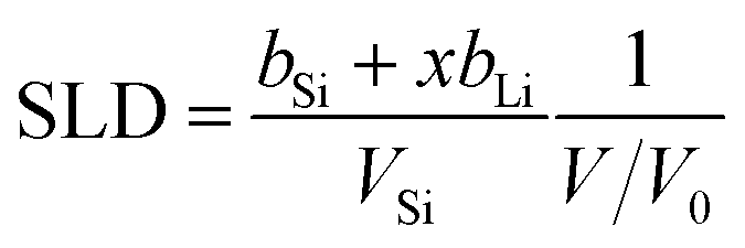 | (1) |
A fundamental reason for the hysteretic behaviour of the capacity (and consequently also of the volume and SLD) can be found in the fact that electrochemical lithiation/delithiation is a non-equilibrium process (non-equilibrium potentials are measured). However, in the present case the electrode was cycled with a low scan rate of 0.01 mV s−1 and only low current densities below 10 μA cm−2 are reached. Consequently, we assume that we are close to equilibrium potentials and the contribution of overpotentials is small.
A possible reason for the observed hysteresis might be correlated to the SEI. The SEI forms an additional internal resistance for the ionic current (e.g. slow diffusion of the Li+ ions through the SEI). If this resistance changes during cycling due to the observed formation and modification of the SEI thickness a hysteretic effect may occur between the capacity and potential. However, the main modification of the SEI takes place during the first cycle, while the hysteretic effect shows no significant difference for both cycles making this explanation unlikely.
Another possible reason for the observed hysteresis is discussed in the literature, where an important role of mechanical stress is indicated. Yoon et al.48 observed in their work also such a hysteresis effect between the volume expansion/charge capacity and electrode potential of an amorphous silicon thin film electrode. They cycled galvanostatically an electrode to a certain potential and held the potential until the initial current decreased to an equilibrium value. In this state they measured the thickness of the specially designed electrode film by atomic force microscopy. They explained the observed hysteresis effect in terms of a stress–potential coupling during lithiation/delithiation based on ref. 49 and 50. Sethuraman et al.51 investigated the stress evolution of thin amorphous films during galavanostatic lithiation/delithiation using an in situ multi-beam laser sensor technique. They found that during lithiation the thin silicon electrode undergoes biaxial compressive elastic stress up to −1.75 GPa until plastic deformation starts in order to accommodate the enormous volume expansion. During delithiation tensile stress up to 1 GPa occurs. Additional mechanical work is needed to insert/remove Li into/from a stressed solid, which has to be delivered by the potentiostat. Sethuraman et al.49,50 estimated the potential change due to biaxial stresses at about 0.1 V GPa−1. In this context, compressive stress lowers the potential while tensile stress raises the potential at a given state of charge of the electrode. Assuming a maximum compressive stress of −1.75 GPa and a tensile stress of 1 GPa to be present during our CV experiments, there should be a difference of 0.275 V between the lithiation and delithiation potential for the same volume value. This is in agreement with Fig. 4(a), where values between 0.2 and 0.35 V were found for relative volume modifications.
Recently published work by Lu et al.52 investigated also the impact of mechanical stress on the voltage hysteresis of thin film amorphous silicon electrodes during galvanostatic lithiation/delithiation experimentally and theoretically. They modified the Butler–Volmer equation, incorporating mechanical stress into the reaction kinetics. They found that mechanical stress can influence the rate of electrochemical reactions at the solid/electrolyte surface in such a way that tensile stress would facilitate lithiation and impede delithiation and vice versa. They carried out galvanostatic experiments at low C/40 rates and observed a hysteretic behaviour of electrode potential versus capacity. They came also to the conclusion that this behaviour is mainly affected by the stress evolution during the galavanostatic lithiation\delithiation process. Similar calculations of stress effects on voltage hysteresis under thermodynamically non-equilibrium conditions were done by Song et al.53 using a diffusion–reaction–stress coupling model. Based on these results we trace back the hysteresis effect in the volume and SLD observed during the CV measurements to be due to such mechanical stress effects.
For further analysis, the relative volume change of the whole electrode plotted as a function of x (in a-LixSi) for the two cycles is shown in Fig. 6(a). The relative Li concentration x was calculated according to
 | (2) |
487 C mol−1 is the Faraday constant, and MSi = 28.09 g mol−1 is the molar mass of silicon. The current I for a given time t is obtained from Fig. 1(a).
 | ||
| Fig. 6 (a) Relative volume changes (V/V0) of the a-LixSi layer as a function of Li content x. The line shows atomistic calculations, as given by Huang and Zhu in ref. 54. Literature data from galvanostatic lithiation experiments are also shown (Jerliu et al. 2014), ref. 20. (b) Scattering length density (SLD) of the a-LixSi layer as a function of Li content x. The black line in (b) corresponds to the SLD calculated from the line in (a) as described in the text. | ||
Also shown in Fig. 6(a) are theoretically calculated volume expansion data of ref. 54 and experimental data measured during galvanostatic cycling for x > 0.5.20 The results of this work are close to these literature data. However, in this context the slope of the volume–composition curve for x > 0.5 is of higher importance. This slope corresponds to the volume increase per inserted lithium atom normalized to the initial volume. From the two lithiation cycles of the CV experiments we get for x > 0.5 identical slopes of 0.80 ± 0.05 and 0.82 ± 0.05 in good agreement with the calculations of ref. 54, where a value of 0.87 was found. Jerliu et al.20 found a slope of ∼0.80 ± 0.05 during galvanostatic lithiation for x > 0.5 which is also in excellent agreement. For the two delithiation cycles during the CV measurement we observe in the composition range x between 0.5 and 3 a deviation from the linear lithiation behaviour. The relative volume is higher in that range if the relative volume is compared for the same Li content x (same state of charge). A possible explanation might be that the extraction of lithium from the electrode is accompanied by an incomplete structural relaxation of the a-LixSi structure. For example, nano-scaled pores or regions of lower density might be formed locally within the structure, giving rise to higher volumes than expected by lithiation. A decision of whether such density variations are only temporarily present and relax during further delithiation or whether they are permanent until complete delithiation is reached cannot be decided from Fig. 6(a). The formation and modification of pores is also supported by the literature. Choi and coworkers55 demonstrated that during electrochemical lithiation/delitiation silicon nanowires become more porous. Pores were also recently observed by Reyes Jimenez et al.56 in amorphous silicon layers (140 nm) after 150 cycles by Focus Ion Beam (FIB) cross-sectional micrography. Further, DeCaluwe et al.25 suggested that macroscopic volume expansion is governed by a pore collapse and regrowth mechanism. During delithiation, the decrease in volume is accompanied by the re-growth of collapsed pores.
The dependence of the SLD of the a-LixSi layer on the Li concentration x for the two cycles is shown in Fig. 6(b). Here, also the SLD is higher during delithiation between x = 0.5 and 3. In the framework of the upper concept, this can be explained by the fact that open porosity is present/formed during delithiation, which is filled with electrolyte with a SLD of 1.75 × 10⁻⁶ Å−2. This will enhance the overall SLD compared to empty pores. Also shown is the theoretical SLD calculated from eqn (1) based on the relative volume change of Fig. 6(a) and ref. 54. There, for values around x = 4 the theoretical data are lower than the experimental data. This is due to the fact that in Fig. 6(a) the experimentally found relative volume is lower than the theoretical one in that range, which is reflected also in the SLD according to eqn (1).
Finally, we discuss the formation and modification of the surface layer associated with the SEI. The SEI forms during the first lithiation cycle as can be seen in Fig. 4(c). For potentials below 0.5 V the thickness of the SEI starts to increase until a maximum value of 120 Å is reached. During delithiation the layer decreases again until a final value of 70 Å is reached after complete delithiation. During the second cycle this phenomenon is much less pronounced. A reversible increase and decrease between 70 Å and 120 Å is observed, indicating a stable modification of the SEI.
In the literature, the formation of the SEI on amorphous silicon electrodes and its modification during galvanostatic lithiation/delithiation were already investigated by Veith et al.,22 using NR at specific potentials after equilibrium was established (cut off the current at certain potentials). They reported that the SEI thickness decreases as the silicon electrode swells during lithiation and thickens during the delithiation step. This is the opposite behaviour as observed here. We attribute this to the use of a different electrolyte (1.2 M LiPF6 ethylene carbonate (EC)/dimethyl carbonate (DMC) 3:7 wt%), which may result in a different composition of the SEI and a different modification during cycling. A discrepancy is also found in the SLD of the SEI that is ranging between 2 × 10⁻⁶ Å−2 and 4 × 10⁻⁶ Å−2 in the work of Veith et al.22 compared to values found here of 0.4 × 10⁻⁶ Å−2 to 1.2 × 10⁻⁶ Å−2. In a different study24 of the same group, where fluorinated ethylene carbonate was used as an additive to the electrolyte, also a thickening of the SEI was found during lithiation by some tenths of a nanometre and a reduction during delithiation, in qualitative agreement with our work. Fears et al.23 found by NR and X-ray photoelectron spectroscopy (XPS) also SEI growth and shrinkage during electrochemical cycling. The results by ex situ XPS show that the SEI thickness increases during Si lithiation and decreases during delithiation. In contrast, NR indicates the opposite behaviour. As an electrolyte 0.1 M lithium bis(trifluoromethanesulfonyl)imide in deuterated dimethyl perfluoroglutarate was used. These results illustrate the complexity of the problem and the special meaning of the electrolyte. Our operando NR data suggest that the use of a solution of 1 M LiClO4 in propylene carbonate seems to be accompanied by a strong increase of the SEI during first lithiation and a reversible modification between 120 Å and 70 Å during the second cycle.
The formation of the SEI during the first lithiation cycle was also observed by in situ atomic force microscopy on silicon electrodes.57 Breitung et al.57 reported that SEI formation begins before lithiation and tremendous volume expansion of the nanoscaled silicon particles occurs. Up to a potential of ∼0.2 V no remarkable changes in nanoparticle size was observed and after that lithiation of silicon started. Cao et al.58 reported in their in situ X-ray reflectivity measurements on crystalline bulk silicon, the formation and growth of the (inorganic) SEI during lithiation up to a thickness of 70 Å and a decrease of the thickness of the SEI to 40 Å at the end of the delithiation process. This is in qualitative agreement with our results. A similar behaviour is found by Yoon et al.48 also using atomic force microscopy, where the SEI ranges between 150 and 200 nm.
5. Conclusion
In conclusion, the following results were achieved from the operando neutron reflectometry experiments during cyclic voltammetry on amorphous silicon electrodes:(i) The incorporation of lithium into amorphous silicon thin film electrodes can effectively be monitored due to a modification of the relative volume and scattering length density (SLD).
(ii) Changes of volume and SLD occur preferably around current extrema of the CV curves observed during lithiation (<0.3 V) and delithiation (>0.2 V).
(iii) Irreversible capacity losses could be identified which were caused by Li stored in the surface layer (SEI) and in the silicon electrode.
(iv) During lithiation we observe a volume expansion of the lithiated a-LixSi up to 390%, which is in first approximation independent of the cycle number. During lithiation a linear relationship between relative volume changes (V/V0) and Li content is observed for x > 0.5. The results are in good agreement with atomistic simulations54 and with results on galvanostatic lithiation experiments20 as given in the literature. During delithiation we find an enhanced volume between x = 0.5 and 3 that is explained by the formation of pores.
(v) During the first lithiation step (starting at 0.5 V) the growth of a several nanometer thin SEI to about 120 Å is observed, which can tentatively be identified with the solid electrolyte interface (SEI). Afterwards a reversible decrease during delithiation and increase during lithiation between 120 Å and 70 Å are found.
(vi) Strong hysteresis effects of relative volume, charge capacity and SLD versus electrode potential were observed and explained to result from mechanical stress.
Conflicts of interest
There are no conflicts to declare.Acknowledgements
Financial support from the Deutsche Forschungsgemeinschaft (DFG) is gratefully acknowledged (Schm 1569/25). We thank the Helmholtz-Zentrum Berlin für Materialien und Energie for providing beamtime and Dr. Sebastian Risse for his support during the electrochemical measurements.References
- (a) High energy density lithium batteries. Materials, engineering, applications, ed. K. E. Aifantis, R. V. Kumar and S. A. Hackney, Wiley-VCH, Weimheim, 2010 Search PubMed; (b) Lithium-ion batteries. Advanced materials and technologies, ed. X. Yuan, CRC Press Taylor & Francis Group, Boca Raton, USA, 2012 Search PubMed.
- Lithium-ion batteries. Science and technologies, ed. M. Yoshio, Springer, New York NY, 2009 Search PubMed.
- C. Liu, F. Li, L.-P. Ma and H.-M. Cheng, Adv. Mater., 2010, 22, E28–E62 CrossRef PubMed.
- B. Diouf and R. Pode, Renewable Energy, 2015, 76, 375–380 CrossRef.
- F. T. Wagner, B. Lakshmanan and M. F. Mathias, J. Phys. Chem. Lett., 2010, 1, 2204–2219 CrossRef.
- P. G. Bruce, B. Scrosati and J.-M. Tarascon, Angew. Chem., Int. Ed., 2008, 47, 2930–2946 CrossRef PubMed.
- M. T. McDowell, S. W. Lee, W. D. Nix and Y. Cui, Adv. Mater., 2013, 25, 4966–4985 CrossRef PubMed.
- (a) H. Zhao, W. Yuan and G. Liu, Nano Today, 2015, 10, 193–212 CrossRef; (b) M. Winter, J. O. Besenhard, M. E. Spahr and P. Novák, Adv. Mater., 1998, 10, 725–763 CrossRef.
- L. Y. Beaulieu, T. D. Hatchard, A. Bonakdarpour, M. D. Fleischauer and J. R. Dahn, J. Electrochem. Soc., 2003, 150, A1457 CrossRef.
- D. Ma, Z. Cao and A. Hu, Nano-Micro Lett., 2014, 6, 347–358 CrossRef.
- M. Ashuri, Q. He and L. L. Shaw, Nanoscale, 2016, 8, 74–103 RSC.
- E. Pollak, G. Salitra, V. Baranchugov and D. Aurbach, J. Phys. Chem. C, 2007, 111, 11437–11444 CrossRef.
- J. W. Kim, J. H. Ryu, K. T. Lee and S. M. Oh, J. Power Sources, 2005, 147, 227–233 CrossRef.
- (a) B. Liang, Y. Liu and Y. Xu, J. Power Sources, 2014, 267, 469–490 CrossRef; (b) M. Ko, S. Chae and J. Cho, ChemElectroChem, 2015, 2, 1645–1651 CrossRef PubMed.
- (a) J. R. Szczech and S. Jin, Energy Environ. Sci., 2011, 4, 56–72 RSC; (b) J.-Y. Li, Q. Xu, G. Li, Y.-X. Yin, L.-J. Wan and Y.-G. Guo, Mater. Chem. Front., 2017, 414, 359 Search PubMed.
- F. Ozanam and M. Rosso, Mater. Sci. Eng., B, 2016, 213, 2–11 CrossRef.
- (a) S. Bourderau, T. Brousse and D. M. Schleich, J. Power Sources, 1999, 81–82, 233–236 CrossRef; (b) H. Jung, M. Park, S. H. Han, H. Lim and S.-K. Joo, Solid State Commun., 2003, 125, 387–390 CrossRef; (c) S. Ohara, J. Suzuki, K. Sekine and T. Takamura, J. Power Sources, 2004, 136, 303–306 CrossRef; (d) Lithium Batteries. Science and Technology, ed. G.-A. Nazri and G. Pistoia, 2003 Search PubMed; (e) T. Takamura, S. Ohara, M. Uehara, J. Suzuki and K. Sekine, J. Power Sources, 2004, 129, 96–100 CrossRef.
- V. Baranchugov, E. Markevich, E. Pollak, G. Salitra and D. Aurbach, Electrochem. Commun., 2007, 9, 796–800 CrossRef.
- B. Jerliu, L. Dörrer, E. Hüger, B.-K. Seidlhofer, R. Steitz, G. Borchardt and H. Schmidt, Int. J. Mater. Res., 2017, 108, 999 Search PubMed.
- B. Jerliu, E. Hüger, L. Dörrer, B.-K. Seidlhofer, R. Steitz, V. Oberst, U. Geckle, M. Bruns and H. Schmidt, J. Phys. Chem. C, 2014, 118, 9395–9399 CrossRef.
- B.-K. Seidlhofer, B. Jerliu, M. Trapp, E. Hüger, S. Risse, R. Cubitt, H. Schmidt, R. Steitz and M. Ballauff, ACS Nano, 2016, 10, 7458–7466 CrossRef PubMed.
- G. M. Veith, M. Doucet, J. K. Baldwin, R. L. Sacci, T. M. Fears, Y. Wang and J. F. Browning, J. Phys. Chem. C, 2015, 119, 20339–20349 CrossRef.
- T. M. Fears, M. Doucet, J. F. Browning, J. K. S. Baldwin, J. G. Winiarz, H. Kaiser, H. Taub, R. L. Sacci and G. M. Veith, Phys. Chem. Chem. Phys., 2016, 18, 13927–13940 RSC.
- G. M. Veith, M. Doucet, R. L. Sacci, B. Vacaliuc, J. K. Baldwin and J. F. Browning, Sci. Rep., 2017, 7, 6326 CrossRef PubMed.
- S. C. DeCaluwe, B. M. Dhar, L. Huang, Y. He, K. Yang, J. P. Owejan, Y. Zhao, A. A. Talin, J. A. Dura and H. Wang, Phys. Chem. Chem. Phys., 2015, 17, 11301–11312 RSC.
- B. Jerliu, L. Dörrer, E. Hüger, G. Borchardt, R. Steitz, U. Geckle, V. Oberst, M. Bruns, O. Schneider and H. Schmidt, Phys. Chem. Chem. Phys., 2013, 15, 7777–7784 RSC.
- T. D. Hatchard and J. R. Dahn, J. Electrochem. Soc., 2004, 151, A838 CrossRef.
- D. S. M. Iaboni and M. N. Obrovac, J. Electrochem. Soc., 2015, 163, A255–A261 CrossRef.
- A. Nelson, J. Appl. Crystallogr., 2006, 39, 273–276 CrossRef.
- V. P. Phan, B. Pecquenard and F. Le Cras, Adv. Funct. Mater., 2012, 22, 2580–2584 CrossRef.
- T. L. Kulova, Russ. J. Electrochem., 2008, 44, 525–529 CrossRef.
- H. Xia, S. Tang and L. Lu, Mater. Res. Bull., 2007, 42, 1301–1309 CrossRef.
- H. Guo, H. Zhao, C. Yin and W. Qiu, Mater. Sci. Eng., B, 2006, 131, 173–176 CrossRef.
- K. W. Schroder, H. Celio, L. J. Webb and K. J. Stevenson, J. Phys. Chem. C, 2012, 116, 19737–19747 CrossRef.
- L. B. Chen, J. Y. Xie, H. C. Yu and T. H. Wang, J. Appl. Electrochem., 2009, 39, 1157–1162 CrossRef.
- A. Reyes Jiménez, R. Klöpsch, R. Wagner, U. C. Rodehorst, M. Kolek, R. Nölle, M. Winter and T. Placke, ACS Nano, 2017, 11, 4731–4744 CrossRef PubMed.
- K. W. Schroder, A. G. Dylla, S. J. Harris, L. J. Webb and K. J. Stevenson, ACS Appl. Mater. Interfaces, 2014, 6, 21510–21524 CrossRef PubMed.
- T. Kim, S. Park and S. M. Oh, J. Electrochem. Soc., 2007, 154, A1112 CrossRef.
- C. Pereira-Nabais, J. Światowska, A. Chagnes, F. Ozanam, A. Gohier, P. Tran-Van, C.-S. Cojocaru, M. Cassir and P. Marcus, Appl. Surf. Sci., 2013, 266, 5–16 CrossRef.
- W. J. Weydanz, M. Wohlfahrt-Mehrens and R. A. Huggins, J. Power Sources, 1999, 81–82, 237–242 CrossRef.
- (a) C. J. Wen and R. A. Huggins, J. Solid State Chem., 1981, 37, 271–278 CrossRef; (b) R. A. Sharma, J. Electrochem. Soc., 1976, 123, 1763 CrossRef; (c) N. Dimov, S. Kugino and M. Yoshio, Electrochim. Acta, 2003, 48, 1579–1587 CrossRef.
- W.-J. Zhang, J. Power Sources, 2011, 196, 13–24 CrossRef.
- G. M. Veith, L. Baggetto, R. L. Sacci, R. R. Unocic, W. E. Tenhaeff and J. F. Browning, Chem. Commun., 2014, 50, 3081–3084 RSC.
- J. W. Wang, Y. He, F. Fan, X. H. Liu, S. Xia, Y. Liu, C. T. Harris, H. Li, J. Y. Huang, S. X. Mao and T. Zhu, Nano Lett., 2013, 13, 709–715 CrossRef PubMed.
- K. Xu, J. Electrochem. Soc., 2009, 156, A751 CrossRef.
- C. Cao, H.-G. Steinrück, B. Shyam, K. H. Stone and M. F. Toney, Nano Lett., 2016, 16, 7394–7401 CrossRef PubMed.
- B. Jerliu, E. Hüger, M. Horisberger, J. Stahn and H. Schmidt, J. Power Sources, 2017, 359, 415–421 CrossRef.
- I. Yoon, D. P. Abraham, B. L. Lucht, A. F. Bower and P. R. Guduru, Adv. Energy Mater., 2016, 6, 1600099 CrossRef.
- G. Bucci, S. P. V. Nadimpalli, V. A. Sethuraman, A. F. Bower and P. R. Guduru, J. Mech. Phys. Solids, 2014, 62, 276–294 CrossRef.
- V. A. Sethuraman, V. Srinivasan, A. F. Bower and P. R. Guduru, J. Electrochem. Soc., 2010, 157, A1253 CrossRef.
- V. A. Sethuraman, M. J. Chon, M. Shimshak, V. Srinivasan and P. R. Guduru, J. Power Sources, 2010, 195, 5062–5066 CrossRef.
- B. Lu, Y. Song, Q. Zhang, J. Pan, Y.-T. Cheng and J. Zhang, Phys. Chem. Chem. Phys., 2016, 18, 4721–4727 RSC.
- Y. C. Song, A. K. Soh and J. Q. Zhang, J. Mater. Sci., 2016, 51, 9902–9911 CrossRef.
- S. Huang and T. Zhu, J. Power Sources, 2011, 196, 3664–3668 CrossRef.
- J. W. Choi, J. McDonough, S. Jeong, J. S. Yoo, C. K. Chan and Y. Cui, Nano Lett., 2010, 10, 1409–1413 CrossRef PubMed.
- A. Reyes Jiménez, R. Nölle, R. Wagner, J. Hüsker, M. Kolek, R. Schmuch, M. Winter and T. Placke, Nanoscale, 2018, 10, 2128–2137 RSC.
- B. Breitung, P. Baumann, H. Sommer, J. Janek and T. Brezesinski, Nanoscale, 2016, 8, 14048–14056 RSC.
- C. Cao, H.-G. Steinrück, B. Shyam and M. F. Toney, Adv. Mater. Interfaces, 2017, 154, 1700771 CrossRef.
- Scattering Length Density Calculator, available at: https://www.ncnr.nist.gov/resources/sldcalc.html, accessed5 September 2017.
- N. N. Greenwood and A. Earnshaw, Chemistry of the elements, Pergamon Press, Oxford u.a., 1st edn, 1984 Search PubMed.
- Copper – Element information, properties and uses|Periodic Table, available at: http://www.rsc.org/periodic-table/element/29/copper, accessed 5 September 2017.
- Z. Remeš, M. Vaněček, P. Torres, U. Kroll, A. H. Mahan and R. S. Crandall, J. Non-Cryst. Solids, 1998, 227–230, 876–879 CrossRef.
- W. M. Haynes, CRC Handbook of Chemistry and Physics, CRC Press, Hoboken, 92nd edn, 2011 Search PubMed.
Footnote |
| † Electronic supplementary information (ESI) available. See DOI: 10.1039/c8cp03540g |
| This journal is © the Owner Societies 2018 |