
 Open Access Article
 This Open Access Article is licensed under a
 Creative Commons Attribution 3.0 Unported Licence
Lithium permeation within lithium niobate multilayers with ultrathin chromium, silicon and carbon spacer layers†
Erwin
Hüger
 *a,
Lars
Dörrer
a,
Rattikorn
Yimnirun
b,
Jaru
Jutimoosik
c,
Jochen
Stahn
d and
Amitesh
Paul
e
*a,
Lars
Dörrer
a,
Rattikorn
Yimnirun
b,
Jaru
Jutimoosik
c,
Jochen
Stahn
d and
Amitesh
Paul
e
aInstitute of Metallurgy, Microkinetics Group, Clausthal University of Technology, Robert-Koch-Str. 42, D-38678 Clausthal Zellerfeld, Germany. E-mail: erwin.hueger@tu-clausthal.de
bSchool of Energy Science and Engineering, Vidyasirimedhi Institute of Science and Technology, Wang Chan Valley, Rayong 21210, Thailand
cDepartment of Physics, Faculty of Science, Naresuan University, Phitsanulok, 65000, Thailand
dLaboratory for Neutron Scattering and Imaging, Paul-Scherrer-Institut, CH-5232 Villigen PSI, Switzerland
eTechnische Universität München, Physik Department E21, Lehrstuhl für Neutronenstreuung, James-Franck-Straße 1, D-85748 Garching, Germany
First published on 3rd September 2018
Abstract
Li permeation through ultrathin Cr, Si and C layers and interfaces is of interest in the optimization of lithium ion batteries with respect to the control of Li flux. Twenty-one LiNbO3 layers (9 nm), which serve as solid state Li reservoirs, were sputter deposited in an alternating sequence of enriched 6Li or 7Li isotope fractions spaced with (8 nm) thin Cr, Si and C layers. The Li isotope contrast was used to measure Li permeation using depth profiling by secondary ion mass spectrometry and neutron reflectometry on a nanometer scale. Extremely low Li permeation for Cr and Si at room temperature exemplifies the effective blocking of Li movement at least for five years. However, Li permeation through C layers was found to be faster than through Cr and Si layers. With temperature, the Li permeation is enhanced through Cr as compared to that through Si layers. Furthermore, material characterisation shows amorphous LiNbO3, C and Si layers and polycrystalline Cr layers (with 80% elemental bcc chromium and 20% chromium-oxide situated at Cr/LiNbO3 interfaces). Annealing in air at 100 °C (373 K) does not oxidize the Cr layers any further. A stress of 12 GPa, which was measured in Cr spacer layers at room temperature, remains unchanged upon annealing. The origin of a weak ferromagnetic order measured at room temperature (300 K) was attributed to some traces of Cr and Si inside LiNbO3.
1. Introduction
Artificial multilayers1,2 present an opportunity to design stable structures with non-equilibrium properties different from the bulk forms of their components.3–12 The more different the properties of alternating layers are, the more surprising can be the properties of a whole multilayer. The proximity of an electronic insulator to a pure electronic conductor can lead to spatially separated ultrafast (dual) transport pathways of electrons and ions with ionic diffusion coefficients higher than in liquids.12 Therefore, synergistic, ultrafast mass storage and consequent removal in artificially mixed materials can appear.12 Obviously, most of the generated properties stem from the proximity of different materials in a multilayer, i.e. from interfaces.10–13Superlattices possess a large number of interfaces, enhancing possible usage of interface generated properties. For example, space charge layers can appear on Schottky contact types of interfaces which strongly affect nanoionics and charge transport phenomena.14–36 On Schottky-contact like interfaces, the electronic band structure is locally disturbed by band bending. Furthermore, quantum size effects can appear in ultrathin layers, which also change the electronic band structure according to the quantum well state requirements.37 The changes in band structure can change the density of states at the Fermi energy. This can generate properties different to those known for the materials of the constituent layers.38–42
In general, oxide and non-oxide materials possess a strong contrast in properties. Most prominent oxides, such as silica and lithium niobate (LiNbO3), are insulators, whereas typical non-oxide materials, such as d-band metals (e.g. Cr), are good electrical conductors. This work reports on the fabrication and characterization of multilayers which combine LiNbO3 with chromium, silicon and carbon layers. It is shown that laminar structures of alternating ultrathin layers of amorphous LiNbO3 and Cr, Si and C material are stable and enable the measurement of Li permeation through these layers and interfaces which is of interest for lithium ion batteries with respect to the control of Li flux. The knowledge of the Li permeation strength enables understanding of the mechanism and kinetics of electrochemical Li storage in electrodes.80
Coating of Li ion battery electrodes with thin films43–47 is a strategy to improve the operation, such as the lifespan of next generation lithium-ion batteries for high power application. Beside carbon,43 chromium44–47 coating is also a route to produce operable Li-ion batteries with negative electrodes possessing Si as the active material. Silicon has the highest known gravimetric capacity to store electrical energy (Li ions) up to the Li4.4Si alloy.48,49 Unfortunately, at such a huge Li storage the Li–Si active material expands by nearly 400%. Research using silicon materials has experienced that cycling pulverizes the silicon electrode, rapidly reducing its overall capacity by silicon delamination from the current collector. To avoid this deficiency, Cr-coated nano-silicon (e.g. Si nano-powder) cells, for example, are found to be superior to uncoated cells for battery operation.46,47 Moreover, it is claimed that the coating of electrodes with Cr enables the storage of a larger amount of Li in the active material of the battery.47 Furthermore, the battery operation characteristics were found to be enhanced when the positive electrode is also coated with Cr.50 Recently,43,45 it was shown that a multilayer architecture comprising of C/Si43 and Cr/Si45 multilayers is a novel strategy for addressing the extreme challenges associated with high energy storage materials in Li-ion batteries. Chromium does not store Li, i.e. it does not lithiate. In the lithiation and delithiation process of Cr (and C) coated electrodes (Si nanopowder, and Cr/Si and C/Si multilayers), Li has to permeate through the Cr (C) spacer layers in order to be stored or removed from the active materials of electrodes.
For energy devices such as batteries, there is a huge effort to reduce the inactive material of a battery by using ultrathin layers. Chromium layers with thicknesses in between 2 and 15 nm are used to increase the adhesion of the metallic current collector (such as Au, Cu, and Pt films) to the packaging support (e.g. ceramic materials).51–54 The Cr layer is in between the current collector and the packaging support and is also in between the current collector and the active (e.g. Si) material.53 There is a stringent condition which dictates that Li should not penetrate the current collector (and the Cr layer) so that it does not reach the packaging support (glass silica) where it eventually gets lost. The capacity loss seen upon cycling lithium ion batteries (LIBs) was recently attributed to diffusive loss of Li in current collectors.83,84 Li that has reached the current collector (or the Cr layer) is no more in an ionic state. In that case, the Li permeation happens only by Li diffusion without an electrical driving force. Thereby, experiments of Li permeation through thin Cr layers without an electrical driving force are necessary. Such Li permeation experiments are presented in this work.
With regards to size effects on charge transport, one has to mention that the electronic industry worldwide possess a pressing need to reduce the dimensions of integrated circuit components to below 10 nm.55 Unfortunately, this trend is coming to stagnancy because the resistivity of the transistor interconnects increases with shrinking dimensions.55 The capability of nano-sized metals to conduct electronic charge decreases if the shrinking dimension is in the nanoscale regime (e.g. below 38 nm for copper).55 The aim of the present work is (i) to investigate the capability of nano-sized metal to conduct Li and (ii) to analyse the properties of the material through which Li permeation can be measured. Recently, Hüger et al. introduced multilayers which combine amorphous LiNbO3 layers with Si spacer layers (i.e. [LiNbO3/Si] multilayers) to measure Li permeation through Si layers.56 In this work we provide additional insights into this new class of multilayers and LiNbO3 layers spaced by ultrathin chromium and carbon layers. These results are compared to Li conductivity through ultrathin Si layers. In all cases, Li permeation was measured without applying an electrical driving force.
2. Materials and methods
Multilayers as sketched in Fig. 1 were deposited using an ion-beam coater (IBC 681) from Gatan, Inc. (Pleasanton, CA, USA). The depositions were performed at room temperature.2 The multilayer samples were stored in air and at room temperature (300 K). Annealing was performed at 1 mbar using a drying furnace. Synchrotron extended X-ray absorption fine structure spectroscopy (EXAFS) measurements were performed in situ during Li permeation at 100 °C (373 K) at SRLI, Thailand. All other measurements were performed at room temperature.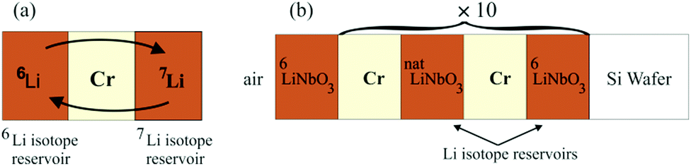 | ||
| Fig. 1 (a) Basic principle of the experimental arrangement: two Li isotope reservoir layers are spaced by a Cr (or Si or C) layer. (b) Sketch of the multilayer produced for NR measurements. | ||
There are not many measurement techniques sensitive to light elements such as lithium. We apply two techniques with proper sensitivity for lithium (also isotope) detection, neutron reflectometry (NR)85 and secondary ion mass spectrometry (SIMS).86 SIMS was applied to determine primarily the Li isotope depth profile of the multilayer. Furthermore, profound investigations were performed also with X-ray reflectivity (XRR), grazing incidence X-ray diffraction (GI-XRD), Fourier transform infrared spectroscopy (FTIR), Raman scattering, and EXAFS with details given in the ESI accompanying this work.2 Magnetisation curves were measured using a superconducting quantum interference device (SQUID) from Quantum Design (MPMS-XL).
3. Results and discussion
Fig. 1a sketches the basic structure used for the investigations of Li transport through thin spacer layers. It consists of a triple layer form of 7LiNbO3/spacer-layer/6LiNbO3 with single layer thicknesses of up to 10 nm. Here, two isotope enriched lithium niobate layers are placed adjacent to a Cr (Si or C) layer. The lithium niobate layers serve as solid state Li reservoirs. Annealing leads to a mutual exchange of Li isotopes through the spacer layers and adjacent interfaces by Li permeation and thus to a leveling of the isotope fractions. The Li kinetics is obtained by measuring the fraction of 6Li and 7Li isotopes in the Li reservoirs. The multilayer sketched in Fig. 1b with twenty (LiNbO3/spacer-layer) double layers was used for NR experiments.2 Visualization of the multilayer stack with up to 10 nm thin layers is achieved even with optical microscopy as presented in the ESI.23.1 Atomic and isotope depth profiling performed with SIMS
Fig. 2 and 3 represent the 6Li/7Li isotope contrast in the LiNbO3 layers of the multilayer with Si, Cr and C spacer layers as measured by SIMS depth profiling. Astounding periodic SIMS signals were measured in the depth profiles for the ML with Si and Cr spacer layers (ESI2). The recorded Li+ SIMS signals are extremely strong. An (O2+, 5 keV) primary ion beam was used for the SIMS measurements presented in the main article. Extensive SIMS data are presented in the ESI.2 A discussion about the destructive nature of SIMS, i.e. the sputtering process, on the depth profiles is also given.26Li (and 7Li) isotope fraction can be obtained from the SIMS signals by the following fraction of SIMS intensities | (1) |
 and
and  are the SIMS intensities measured for the 6Li and 7Li masses, respectively. The obtained Li isotope fraction are presented in Fig. 3. A strong modulation of the Li isotope fraction is measured by SIMS in as-deposited multilayers with Si (Fig. 3a and b) and Cr (Fig. 3c and d) spacer layers.
 | ||
| Fig. 2 SIMS depth profiles of (a, d and g) Li isotope, (b) 28Si, (e) 52Cr, (h) 16O, and (c, f and i) 93Nb masses of the multilayer system with Si (a–c), Cr (d–f) and C (g–i) spacer layers in the as-deposited state after 5 days of storage in air and room temperature (300 K). | ||
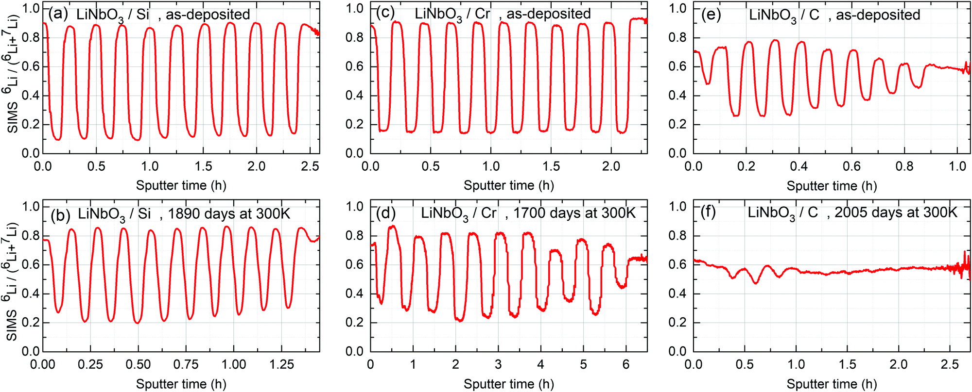 | ||
| Fig. 3 Relative 6Li fraction as obtained from SIMS measurements on multilayers with Si (a and b), Cr (c and d) and C (e and f) spacer layers using eqn (1). (a, c and e) 6Li fraction of the as deposited ML measured after 5 days of storage in air and room temperature (300 K) for the ML with Si (a), Cr (c) and C (e) spacer layers, respectively. (b, d and f) were measured after 1890, 1700 and 2005 days of storage in air and room temperature (300 K) for the ML with Si, Cr and C spacer layers, respectively. In displaying the isotope fraction, it is unnecessary to show the calculated values of both Li6/(Li6 + Li7) and Li7/(Li6 + Li7), because if one of them is χ(t), the other is 1 − χ(t) (see eqn (1)). | ||
3.2 Li permeation at room temperature
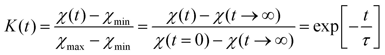
The influence of multilayer storage in air and room temperature for roughly 5 years is presented in Fig. 3. The Li contrast in the ML with carbon spacer layers is diminished (Fig. 3f). The decrease of the 6Li isotope fraction in the 6LiNbO3 layers up to full isotope intermixing is given by (neglecting initial transition times)56,80 | (2) |
 | (3) |
 and
and  are the 6Li isotope fraction in the 6LiNbO3 and the natLiNbO3 layer at t = 0, i.e. before the Li isotope intermixing appears. The quantity τ represents the time-constant of the exponential decay function and is given by56,80
 | (4) |
| P = S·D | (5) |
 | (6) |
 | ||
| Fig. 4 6Li contrast (in percent) of the 6LiNbO3 layers as a function of ML storage time at room temperature (300 K) as obtained from SIMS depth profiles performed on the ML with C spacer layers.2 The line represent the fit of eqn (6) to measured data. | ||
For the multilayer with Si and Cr spacer layers, the Li isotope contrasts are only marginally reduced (Fig. 3). Obviously, Li permeation through carbon layers is faster than through the Si and Cr layers.
Now, from the experiments performed on the multilayers with Si and Cr spacer layers stored at room temperature, one can suspect that the time constant τ for Li permeation is roughly 100 (or more) years. According to eqn (4), a roughly estimated Li permeability of P ≤ 2 × 10⁻²⁷ m2 s−1 is then obtained for the superlattice with Si and Cr spacer layers. This extremely low value corresponds to proper Li blocking. For silicon, the result contributes to an explanation why electrochemical lithiation of Si electrodes in LIBs takes place by a moving phase boundary separating a high lithiated Li–Si phase from a poor or non lithiated Si phase as discussed in ref. 80.
A legitimate question that arises is whether Li transport is controlled by Li flux through the LiNbO3 reservoir layers or by Li permeation through the Cr and Si spacer layers. If Li permeation would be controlled by Li diffusion in the LiNbO3 reservoir layers, then the Li permeation strength should not be dependent on the spacer layer material. The faster Li permeation at room temperature measured for the ML with C (compared to Cr and Si) spacer layers indicates that Li transport is controlled by the Li flux through the spacer layers. This finding is justified also by considering the Li diffusion coefficient in amorphous LiNbO3 measured by Rahn et al.57 for thin films stored at room temperature which amounts to D = 1 × 10⁻¹⁸ m2 s−1. Considering the Li solubility in LiNbO3 to amount to 0.2, a Li permeability of P = 2 × 10⁻¹⁹ m2 s−1 is obtained for the Li flux through the LiNbO3 reservoir layers. This value is eight orders of magnitude larger than the measured Li flux in the multilayers. Hence, the Li diffusion inside the Li reservoirs is not responsible for the observed hindered Li isotope intermixing in Li reservoir layers. The Li blocking effect is due to the (e.g. Si and Cr) spacer layers.
The slow Li permeation through Si and Cr spacer layers at room temperature does not solely mean that the Li diffusivity at room temperature is extremely low. According to eqn (5), the low Li permeability could stem from a very low solubility of Li in silicon and chromium material. The Li solubility in ultrathin amorphous Si and in nanocrystalline Cr layers is unknown, but it can be expected to be in the range of some ppm at room temperature. The phase diagram of Li–Si in the crystalline form does not evidence any LixSi phases for x below 1.7.58–67 The solubility of Li in crystalline silicon was measured to be very low. An extrapolation of the Li solubility in silicon versus inverse temperature 1/T data64–67 to room temperature gives the Li solubility in crystalline Si to be less than 1 ppm. The Li solubility in 95 nm thick amorphous Si layers was measured at temperatures of 240 °C and higher.80 An extrapolation to room temperature gives the Li solubility in thick amorphous Si layers to be extremely low, i.e., 3 × 10⁻⁹ Li per Si atom.80 In the case of chromium, Li does not alloy with it.68,69 There exist reports about only the solubility of Cr in liquid Li.68,69 In similarity to Si, one can expect that the solubility of Li in Cr is also very low. So, in order to induce considerable (measurable) Li permeation through the Si or Cr spacer layers we annealed the samples to enhance Li solubility and diffusivity. The measurements at elevated temperatures were performed non-destructively by neutron reflectometry.
3.3 Atomic and isotope depth profiling performed with neutron scattering for Li permeation measurements
Fig. 5 presents the NR pattern recorded from the 6Li/7Li isotope modulated LiNbO3 superlattice with Cr spacer layers, together with the NR simulation based on the Parratt formalism. Superlattice characteristics such as individual layer thicknesses, neutron scattering length density (SLD) and interlayer roughness corresponding to the best fit of Parratt32 simulation are listed in Table 1. The SLD depth profile is presented in Fig. 5b. | ||
| Fig. 5 (a) Measured NR pattern (open symbols) and corresponding Parratt32 simulations (line) for the superlattice with Cr spacer layers in the as-deposited state. (b) Neutron scattering length density obtained from the NR fit given in panel (a). Fitting parameters are given in Table 1. | ||
| Layer | SLD (10−6 Å−2) | Thickness (nm) | Roughness (nm) | Mass-density (g cm−3) | |
|---|---|---|---|---|---|
| Air | Air | 0 | — | — | — |
| Capping-layer | 6LiNbO3 | 4.45 ± 0.2 | 9.0 ± 0.8 | 3.0 ± 1.0 | 4.17 ± 0.2 |
| Multilayer × 10 | Cr | 3.1 ± 0.1 | 8.2 ± 0.1 | 1.8 ± 0.5 | 7.3 ± 0.3 |
| natLiNbO3 | 3.9 ± 0.05 | 9.0 ± 0.1 | 1.8 ± 0.5 | 4.24 ± 0.1 | |
| Cr | 3.1 ± 0.1 | 8.2 ± 0.1 | 1.8 ± 0.5 | 7.3 ± 0.3 | |
| 6LiNbO3 | 4.45 ± 0.05 | 8.9 ± 0.1 | 1.8 ± 0.5 | 4.17 ± 0.1 | |
| Si-wafer | Si | 2.07 | — | 0.5 | 2.3 |
The Bragg peak located at Qz = 0.039 Å−1 appears due to the double layer periodicity produced by the chemical contrast of Cr and LiNbO3 inside the superlattice.
The periodicity of the Li isotopes produces a four-layer periodicity [Cr/6LiNbO3/Cr/7LiNbO3] in neutron scattering from the superlattice. Consequently, the Bragg peak located at Qz = 0.023 Å−1 appears due to the four-layer periodicity produced by the Li isotope contrast inside the superlattice. In contrast to the SIMS measurements, NR does not give any hints for a double peak structure in the depth profile (Fig. 5b) thanks to the non-destructive nature of the neutrons. More information on this issue is given in ESI.†
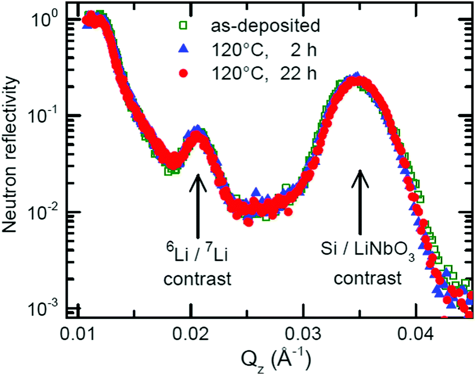
The samples were annealed in order to measure Li permeation within the scheduled neutron beam time. Fig. 6 presents the NR patterns measured from the superlattice with Cr spacer layers after sequential annealing at 100 °C (373 K), together with NR simulation. The total reflection edge (located at Qz = 0.013 Å−1) and the Bragg peak due to chemical contrast (Qz = 0.039 Å−1) do not change at all by annealing at 100 °C (see Fig. 6b). Solely, the Bragg peak due to Li isotope contrast diminishes which is confirmed also by the SIMS data (see Fig. 7b). Li permeation through Cr spacer layers takes place without any other (measurable) changes in the superlattice.
 | ||
| Fig. 6 Measured NR patterns (symbols) of the superlattice with Cr spacer layers in the as-deposited state and after annealing at 100 °C (373 K) for 3.5 h, 7 h, and 11 h. The lines represent the Parratt32 fits to the measured patterns. (a) Reflectivity curves shifted in intensity for a better visualization of the Bragg peak decrease. (b) Non-shifted reflectivity curves for a proper visualization of the lack of changes in the total reflection edge and in the Bragg peak due to chemical contrast. | ||
 | ||
| Fig. 7 6Li fraction measured by SIMS from (a) the ML with Si spacer layers after 22 h of annealing at 120 °C (393 K) and (b) the ML with Cr spacer layers after 11 h of annealing at 100 °C (373 K). | ||
The fits to the measured NR patterns delivered the amount of Li isotope fractions in Li reservoirs. Fig. 8 shows how the Li isotope fraction in Li reservoirs changes with annealing time. The kinetics of Li isotope intermixing enables the determination of Li permeability. A fit of eqn (2) to the measured Li kinetic data of Fig. 8 determined the time constant of Li permeation to be τ = (4.6 ± 0.5) hours. The Li permeability can be determined from eqn (4) to be P = (2 ± 0.5) × 10−22 m2 s−1. The same procedure can be applied to the behaviour of 7Li atoms, which results in the same permeability within error limits.
 | ||
| Fig. 8 Relative 6Li (a) and 7Li (b) fractions of the 6LiNbO3 and natLiNbO3 layers of the superlattice with Cr spacer layers, respectively, as a function of annealing time as obtained from the Parratt32 fits to measured NR patterns (Fig. 6). The lines represent the fit of eqn (2) to measured data. | ||
The Li diffusion coefficient in amorphous LiNbO3 films annealed at 100 °C (373 K) was measured by Rahn et al.57 to be D = 2.6 × 10⁻¹⁶ m2 s−1. Considering the Li solubility in LiNbO3 to amount to 0.2, a Li permeability of P = 5.2 × 10⁻¹⁷ m2 s−1 is obtained for the Li flux through the LiNbO3 reservoir layers at 100 °C (373 K). This value is 5 orders of magnitude higher than that measured here in the superlattice at 100 °C (P = (2 ± 0.5) × 10−22 m2 s−1).
Hence, also at 100 °C, the Li flux in the superlattice is controlled by the Li blocking effect of the Cr spacer layers, i.e. by the Li permeation through Cr layers.
Fig. 9 presents the Li permeation experiments through 9 nm thin Si spacer layers as traced by NR. The experiments revealed that Li permeation through the Si layers is much slower than through the Cr spacer layers. Even a higher annealing temperature (120 °C (393 K)) over a longer annealing time (22 h) does not diminish any NR Bragg peaks, i.e. not even that induced by the Li isotope contrast. This is in agreement with the SIMS depth profiling (see Fig. 7). These experiments show that Si layers are less permeable to Li than Cr layers. The aforementioned experiments at room temperature have shown that Li permeation through C layers is faster than through Cr layers. Hence, Li permeation through Cr layers is faster than through Si layers but slower than through C layers. In turn this evidences that (also above room temperature) Li permeation is not controlled by Li diffusion in LiNbO3 layers.
 | ||
| Fig. 9 NR patterns measured from the multilayer with Si spacer layers after several annealing steps performed at 120 °C. | ||
A possible explanation for the higher Li permeation through the Cr layers in comparison to the Si layers could be different impurity (e.g. oxygen) contents and different crystallographic structures of the Si and Cr layers. It can be expected that the proximity of ultrathin spacer layers to oxide based Li reservoirs oxidizes the spacer layers. In that case, the Li permeation experiments were performed through silicon oxide and chromium oxide78 layers and not through elemental Si and Cr layers. One has to know the material constitution through which Li permeation was measured.
Before doing so, let us mention that the presented methodology can be applied to measure the (diffusion or interface controlled) rate determining step of the Li transport process in nanometer sized layers. Li permeation induces a mutual inter-diffusion of the two different Li isotopes across the interface between the spacer layer (e.g. Cr, Si or C) and the solid state reservoir layer. An interface controlled lithium transport process is evidenced if the transport process lacks a dependence of the lithium isotope exchange rate on the spacer layer thickness. Nonetheless, a diffusion controlled process is expected to show considerable dependence on the spacer layer thickness.2
3.4 Extended characterisation of spacer layers
Investigations by cross sectional TEM would provide direct information on the chemical composition, layer crystallinity, interface roughness and waviness, grain size, boundary and composition. If nothing else, at least this work provides a full characterization of the as-deposited and annealed MLs with a plethora of non-destructive measurement techniques like NR, GI-XRD, FTIR, Raman scattering, X-ray absorption spectroscopy and magnetic measurements. The results are presented in detail in the ESI accompanying this work2 and they are briefly summarized here.Raman scattering found the carbon spacer layers to be amorphous with low sp3 content, as expected for ion beam sputter-deposited carbon coatings. GI-XRD reveals that the LiNbO3, Si and C spacer layers are amorphous whereas the Cr spacer layers are polycrystalline with elemental bcc chromium. There is no evidence of crystalline Cr-oxide. Chromium oxide was also not detected by FTIR and also not by Raman scattering. The neutron SLDs obtained from NR can be explained only with elemental chromium. EXAFS was performed in situ during Li permeation by heating the superlattice to 100 °C (373 K) in air.
The EXAFS experiments revealed the Cr bonding environment to be 80 percent of Cr metal and 20 percent of Cr-oxide with no further evidence of oxidation during the superlattice heating (see Fig. 10). We emphasize that this is not a crystalline phase ratio, but the distinction is based on the atomic neighbourhood derived from XAFS measurements. However, the EXAFS study cannot discern if the measured chromium oxide stems from the Cr layers or from the Cr atoms located inside the LiNbO3 layers. Overall, these experiments evidenced that the ultrathin Cr layers are not (fully) oxidized. The crystallographic network (polycrystalline for Cr layers and amorphous for Si, C and LiNbO3 layers) and the chemistry of the multilayers do not change significantly by the performed Li permeation (i.e. annealing) experiments. GI-XRD experiments measured a high stress of 12 GPa acting on the bcc Cr grains (in the Cr spacer layers of the superlattice) which does not change with the performed Li permeation experiments. Li permeation was measured in an, otherwise, conserved multilayer network.
 | ||
| Fig. 10 Percentage of Cr-metal and Cr2O3 existent in LiNbO3 superlattices with Cr spacer layers as obtained from in situ EXAFS measurements during annealing in air at 100 °C (373 K).2 The inset graph shows in situ measured EXAFS data (circles) with the corresponding combination fit data (line). | ||
However, one may note that the large stress of 12 GPa measured in the Cr spacer layer can be a symptom that the piezoelectric material of the LiNbO3 layers is under strain. The strain can induce a piezoelectric electric field over the (e.g. Cr) spacer layer which can promote or suppress the Li ion transport.81,82 This is of importance for self-charging LIBs that hybridize mechanical energy harvesting and ion storage processes into one process.81,82
Fig. 11 presents the measured magnetic m(H) characteristics at room temperature of the multilayers with Cr, Si and C spacer layers. They show a clear diamagnetic response due to (at least) the diamagnetic Si wafer substrate (see panels a, c, e of Fig. 11). The diamagnetic contribution is overlapped by a magnetic hysteresis for the multilayers with Cr and Si spacer layers (e.g.Fig. 11b and d, respectively). Small magnetic moments can be caused by traces of magnetic impurities (Fe, Co and/or Ni) introduced into the sample during the sample handling or multilayer deposition.71,72 For example, a small amount of Fe, Co or Ni is perhaps incorporated in the multilayer during ML deposition from the IBS sputter chamber walls and/or from the target holder and sample holder. In that case, it should have been expected that the ML with carbon spacer layers should also show a ferromagnetic contribution in the SQUID measurement. The latter is not the case (see Fig. 11e and f) here. Hence, a ferromagnetic spin alignment, caused by Cr and Si elements in the multilayers with Cr and Si spacer layers, cannot be ruled out.
 | ||
| Fig. 11 Magnetic response m(H) measured at room temperature of LiNbO3 multilayers with Cr (a and b), Si (c and d) and C (e and f) spacer layers. (b, d and f) Magnetic characteristics on an enlarged scale for better visualisation of magnetic hysteresis. | ||
Earlier, unexpected ferromagnetism at room temperature was measured in Cr72–76 and Si77 doped thin films of non-ferromagnetic nitrides and oxides. The observed ferromagnetism can be correlated to structural defects induced by the doping species (i.e. Cr and Si). Similarly, the measured magnetic hysteresis in Fig. 11b and d could stem from the presence of Cr and Si inside the LiNbO3 layers. Interface related ferromagnetism can appear by a charge transfer mechanism.72,79 This means that the space charge layers in between LiNbO3 and Cr (and Si) can induce ferromagnetic order in the layers. One may note that, due to the ultrathin fashion of the layers, the space charge layer can extend throughout the entire ultrathin layers.22,23 An electric field over the spacer layer can appear also due to the piezoelectric property of the LiNbO3 layers. The large stress of 12 GPa measured by X-ray scattering (GIXRD) in the Cr spacer layers may be evidence that the piezoelectric material of the LiNbO3 layers is under strain. The strain can induce a piezoelectric electric field over the (e.g. Cr) spacer layer,81,82 which can affect the electronic structure of the spacer layer. Further discussion on magnetic behaviour is given in the related ESI.2
The class of multilayers presented in this work opens up the possibility to investigate the influence of (i) layer chemistry and layer thicknesses, (ii) additional mechanical stress imposed on the multilayers by using sample bending devices, and (iii) the annealing temperature and annealing time interval, on multilayer properties such as magnetism and on the ability to measure Li permeation.
Before concluding let us discuss if the measured spacer layer characteristics might help to explain the measured Li permeation strength. Li permeation through carbon layers was found to be faster than through chromium layers and the latter to be faster than through silicon layers. The difference in Li permeability might occur due to different diffusivities (D). According to eqn (5) (P = SD), the Li permeability (P) also increases if the Li solubility (S) increases for a constant diffusivity. Chromium layers were found to be polycrystalline, whereas the silicon layers were found to be amorphous. The structure of the carbon layers was found to be amorphous with a predominantly graphitic like (sp2 hybridization) configuration and in that manner to be low density carbon. Carbon atoms in a graphitic structure are arranged in parallel densely packed hexagonal atomic layers. There is no chemical bonding between the hexagonal layers and Li can be inserted rather easily between the layers. Consequently, the Li diffusivity and solubility is high in graphitic like carbon. The lithium solubility is well above 10−2 Li per C atom.87,88 This might explain the measured higher Li permeation through carbon spacer layers. In contrast, the Li diffusivity and solubility in amorphous silicon is extremely low.80 The lithium solubility in amorphous silicon should be in the range of 10−9 Li per Si atom,80 and, consequently, more than seven orders of magnitude lower than in carbon. In the case of chromium, as mentioned in Section 3.2, Li does not alloy with it.68,69 In similarity to Si, one can expect that the solubility of Li in Cr is also very low. For the comparison of Li permeation through Cr and Si layers, it is reasonable to assume that Li can diffuse fast along the grain boundaries of the polycrystalline structure of the Cr spacer layers. The grain boundaries might also accommodate a higher amount of Li (increased Li solubility) than the bulk of grains. This is not the case for amorphous silicon. Amorphous Si has no grain boundaries but a continuous covalent network which may serve as an effective barrier for Li permeation.80
4. Conclusions
New layered materials were fabricated by ion beam sputtering deposition of a superlattice with twenty-one thin lithium niobate layers (9 nm) spaced by thin (8 nm) Cr, Si and C spacer layers. The multilayers were primarily used to measure Li permeation through the respective ultrathin Cr, Si and C spacer layers. The LiNbO3 layers serve as Li reservoirs. Each second LiNbO3 layer was enriched with 6Li or 7Li isotopes. The superlattice therefore possesses a Li isotope contrast and a LiNbO3/spacer layer (Cr, Si or C) material contrast. The Li isotope fraction in the multilayer was measured with secondary ion mass spectrometry and neutron reflectometry. Li permeation through the spacer layers changes the Li isotope contrast within the Li reservoirs. This enables us to determine the Li permeability from the time constant of Li isotope contrast change. The measurements were performed without applying an electrical driving force.At room temperature, Li permeation was found to be extremely slow. On the one hand, Li permeation in the ML with C spacer layers diminishes the Li isotope contrast after 5 years of ML storage in air at room temperature. On the other hand, the Li isotope contrast in the MLs with Cr and Si spacer layers is only marginally decreased after 5 years of storage in air at room temperature. From these experiments, a full intermixing of the Li isotopes is expected in some one hundred years for Cr and Si layers at room temperature. The Cr and Si spacer layers are expected to effectively block the Li flux.
Accelerated Li permeation was achieved by annealing treatments. Li permeation through Cr layers at 100 °C (373 K) was measured non-destructively by neutron reflectometry. A full intermixing of the Li isotopes is seen after 11 hours of annealing at 100 °C (373 K). A Li permeability of P = (2 ± 0.5) × 10−22 m2 s−1 was determined from the measured time-constant for Li permeation of τ = (4.6 ± 0.5) hours. The Li permeability value is five orders of magnitude lower than the value of the Li flux through LiNbO3 layers, evidencing that the measured Li permeability stems from the Li permeation through the Cr spacer layers. Overall, Li permeation through C layers was found to be faster than through Cr layers and the latter to be faster than through Si layers. Additional Li permeation experiments are planned to substantiate this statement more quantitatively.
Additional experiments using multiple non-destructive measurement techniques revealed that Li permeation was measured in an, otherwise, conserved multilayer network. The Si and C spacer layers were found to be amorphous, while the Cr spacer layer was found to be polycrystalline with bcc Cr grains. The C spacer layers possess a predominant graphitic like (sp2) bonding configuration. These multilayer characteristics might help to explain the difference of Li permeation found in the spacer layers. Furthermore, the superlattice with Cr spacer layers exercises a high stress of 12 GPa on Cr grains which does not change by Li permeation (i.e. after annealing). Eighty percent of the Cr atoms have a metallic Cr and 20 percent a chromium oxide bonding environment (situated at interfaces). Lastly, a weak ferromagnetic signal at room temperature was measured for the multilayers with Cr and Si spacer layers but not for the multilayers with C spacer layers.
Conflicts of interest
There are no conflicts to declare.Acknowledgements
Financial support from the Deutsche Forschungsgemeinschaft (DFG) under the contract HU 2170/2-1 is gratefully acknowledged. This research project has been supported by the European Commission under the 7th Framework Programme through the ‘Research Infrastructures’ action of the ‘Capacities’ Programme, NMI3-II grant number 283883. This work is based on experiments performed at the Swiss spallation neutron source (SINQ), at the instruments AMOR and Morpheus, PSI Villigen, Switzerland. Thanks are due to H. Schmidt (TU-Clausthal) for the development of the model for Li permeability extraction from measured data, E. Witt and P. Heitjans (U Hannover) for preparing the LiNbO3 sputter targets, K. Bode (TU-Clausthal) for the Raman measurement and M. Opel (TU München) for the SQUID measurements.Notes and references
- The work shows that LiNbO3 multilayers with Cr spacer layers possess crystalline (polycrystalline) Cr layers whereas all layers of the multilayers with alternating Si(C) and LiNbO3 material are amorphous. Hence, throughout this work the terminology of superlattice will be used only for multilayers of alternating Cr and LiNbO3 layers and not for the multilayers of alternating Si(C) and LiNbO3 layers.2.
- Further information is presented in the ESI† accompanying this work. It contains a literature survey, details on multilayer preparation and analysis of microscopy, SIMS, NR, GIXRD, FTIR, Raman scattering and XAS data, and a discussion on magnetic behavior.
- A. K. Yadav, C. T. Nelson, S. L. Hsu, Z. Hong, J. D. Clarkson, C. M. Schlepütz, A. R. Damodaran, P. Shafer, E. Arenholz, L. R. Dedon, D. Chen, A. Vishwanath, A. M. Minor, L. Q. Chen, J. F. Scott, L. W. Martin and R. Ramesh, Nature, 2016, 530, 198 CrossRef PubMed.
- D. Puggioni, G. Giovannetti, M. Capone and J. M. Rondinelli, Phys. Rev. Lett., 2015, 115, 087202 CrossRef PubMed.
- A. Paul, Sci. Rep., 2016, 6, 19315, DOI:10.1038/srep19315.
- Z. Wang, L. P. H. Jeurgens, W. Sigle and E. J. Mittemeijer, Phys. Rev. Lett., 2015, 115, 016102 CrossRef PubMed.
- S. Ghosh, S. Tongay, A. F. Hebard, H. Sahin and F. M. Peeters, J. Magn. Magn. Mater., 2014, 349, 128 CrossRef.
- A. Ohtomo, D. A. Muller, J. L. Grazul and H. Y. Hwang, Nature, 2002, 419, 378 CrossRef PubMed.
- J. S. White, M. Bator, Y. Hu, H. Luetkens, J. Stahn, S. Capelli, S. Das, M. Döbeli, Th. Lippert, V. K. Malik, J. Martynczuk, A. Wokaun, M. Kenzelmann, Ch. Niedermayer and C. W. Schneider, Phys. Rev. Lett., 2013, 111, 037201 CrossRef PubMed.
- F. A. Ma’Mari, T. Moorsom, G. Teobaldi, W. Deacon, Th. Prokscha, H. Luetkens, S. Lee, G. E. Sterbinsky, D. A. Arena, D. A. MacLaren, M. Flokstra, M. Ali, M. C. Wheeler, G. Burnell, B. J. Hickey and O. Cespedes, Nature, 2015, 524, 69 CrossRef PubMed.
- U. Bauer, L. Yao, S. Emori, H. L. Tuller, S. van Dijken and G. S. D. Beach, Nat. Mater., 2015, 14, 174 CrossRef PubMed.
- C.-C. Chen, L. Fu and J. Maier, Nature, 2016, 536, 159 CrossRef PubMed.
- A. Paul, E. Kentzinger, U. Rücker, D. E. Bürgler and P. Grünberg, Phys. Rev. B: Condens. Matter Mater. Phys., 2004, 70, 224410 CrossRef.
- R. T. Tung, Appl. Phys. Rev., 2014, 1, 011304 Search PubMed.
- J. Maier, J. Electroceram., 2015, 34, 69 CrossRef.
- N. Kamaya, K. Homma, Y. Yamakawa, M. Hirayama, R. Kanno, M. Yonemura, T. Kamiyama, Y. Kato, S. Hama, K. Kawamoto and A. Mitsui, Nat. Mater., 2011, 10, 682 CrossRef PubMed.
- M. Ogawa, R. Kanda, K. Yoshida, T. Uemura and K. Harada, J. Power Sources, 2012, 205, 487 CrossRef.
- N. Ohta, K. Takada, I. Sakaguchi, L. Zhang, R. Ma, K. Fukuda, M. Osada and T. Sasaki, Electrochem. Commun., 2007, 9, 1486 CrossRef.
- K. Takada, N. Ohta, L. Zhang, K. Fukuda, I. Sakaguchi, R. Ma, M. Osada and T. Sasaki, Solid State Ionics, 2008, 179, 1333 CrossRef.
- H. Yamada, Y. Oga and I. Moriguchi, J. Electrochem. Soc., 2012, 159, A380 CrossRef.
- D. Ruzmetov, et al. , Nano Lett., 2012, 12, 505 CrossRef PubMed.
- J. Maier, Nat. Mater., 2005, 4, 805 CrossRef PubMed.
- L. A. Haverkate, W. K. Chan and F. M. Mulder, Adv. Funct. Mater., 2010, 20, 4107 CrossRef.
- C. Li, L. Gu, X. Guo, D. Samuelis, K. Tang and J. Maier, Nano Lett., 2012, 12, 1241 CrossRef PubMed.
- K. Takada, N. Ohta and Y. Tateyama, J. Inorg. Organomet. Polym., 2015, 25, 205 CrossRef.
- F. Zhao and A. V. Virkar, J. Power Sources, 2010, 195, 6268 CrossRef.
- L. Fu, C.-C. Chen, D. Samuelis and J. Maier, Phys. Rev. Lett., 2014, 112, 208301 CrossRef.
- J. Maibach, F. Lindgren, H. Eriksson, K. Edström and M. Hahlin, J. Phys. Chem. Lett., 2016, 7, 1775 CrossRef PubMed.
- R. Yu, S. Niu, C. Pan and Z. L. Wang, Nano Energy, 2015, 14, 312 CrossRef.
- S. Kim, J. Fleig and J. Maier, Phys. Chem. Chem. Phys., 2003, 5, 2268 RSC.
- X. Guo, W. Sigle, J. Fleig and J. Maier, Solid State Ionics, 2002, 154–155, 555 CrossRef.
- A. A. Felix, J. L. M. Rupp, J. A. Varela and M. O. Orlandi, J. Appl. Phys., 2012, 112, 054512 CrossRef.
- S. Schweiger, M. Kubicek, F. Messerschmitt, Ch. Murer and J. L. M. Rupp, ACS Nano, 2014, 8, 5032 CrossRef PubMed.
- M. Dawber, K. M. Rabe and J. F. Scott, Rev. Mod. Phys., 2005, 77, 1083 CrossRef.
- V. Ievlev, M. Sumets, A. Kostyuchenko, O. Ovhcinnikov, V. Vakhtel and S. Kannykin, Thin Solid Films, 2013, 542, 289 CrossRef.
- C. Leroux, S. Baudot, M. Charbonnier, A. Van Der Geest, P. Caubet, A. Toffoli, Ph. Blaise, G. Ghibaude, F. Martin and G. Reimbold, Solid-State Electron., 2013, 88, 21 CrossRef.
- E. Hüger and K. Osuch, Eur. Phys. J. B, 2004, 37, 149 CrossRef.
- E. Hüger and K. Osuch, Europhys. Lett., 2003, 63, 90 CrossRef.
- E. Hüger and K. Osuch, Solid State Commun., 2004, 131, 175 CrossRef.
- E. Hüger and K. Osuch, Eur. Phys. J. B, 2004, 44, 145 CrossRef.
- E. Hüger and K. Osuch, Phys. Rev. B: Condens. Matter Mater. Phys., 2005, 72, 085432 CrossRef.
- T. Kana, E. Hüger, D. Legut, M. Cak and M. Sob, Phys. Rev. B, 2016, 93, 134422 CrossRef.
- A. R. Jimenez, R. Klöpsch, R. Wagner, U. Rodehorst, M. Kolek, R. Nölle, M. Winter and T. Placke, ACS Nano, 2017, 11, 4731 CrossRef PubMed.
- D. H. Snydacker, M. Aykol, S. Kirklin and C. Wolverton, J. Electrochem. Soc., 2016, 163, A2054 CrossRef.
- T. T. Fister, J. Esbenshade, X. Chen, B. R. Long, B. Shi, Ch. M. Schlepütz, A. G. Gewirth, M. J. Bedzyk and P. Fenter, Adv. Energy Mater., 2014, 4, 1301494 CrossRef.
- J. K. Lee, B. K. Kim and W. Y. Yoon, Solid State Ionics, 2014, 249–250, 117 Search PubMed.
- S. W. Hwang, J. K. Lee and W. Y. Yoon, J. Power Sources, 2013, 244, 620 CrossRef.
- J. H. Lee, J. K. Lee and W. Y. Yoon, ACS Appl. Mater. Interfaces, 2013, 5, 7058 CrossRef PubMed.
- M. T. McDowell, S. W. Lee, W. D. Nix and Y. Cui, Adv. Mater., 2013, 25, 4966 CrossRef PubMed.
- L. Y. Beaulieu, K. W. Eberman, R. L. Turner, L. J. Krause and J. R. Dahn, Electrochem. Solid-State Lett., 2001, 4, A137 CrossRef.
- S. D. Jones and J. R. Akridge, J. Power Sources, 1993, 44, 505 CrossRef.
- A. Brazier, L. Dupont, L. Dantras-Laffont, N. Kuwata, J. Ka-wamura and J.-M. Tarascon, Chem. Mater., 2008, 20, 2352 CrossRef.
- C. Yu, X. Li, T. Ma, J. Rong, R. Zhang, J. Shaffer, Y. An, Q. Liu, B. Wei and H. Jiang, Adv. Energy Mater., 2012, 2, 68 CrossRef.
- M. E. Holtz, Y. Yu, D. Gunceler, J. Gao, R. Sundararaman, K. A. Schwarz, T. A. Arias, H. D. Abruna and D. A. Muller, Nano Lett., 2014, 14, 1453 CrossRef PubMed.
- R. C. Munoz and C. Arenas, Appl. Phys. Rev., 2017, 4, 011102 Search PubMed.
- E. Hüger, L. Dörrer, J. Rahn, T. Panzner, J. Stahn, G. Lilienkamp and H. Schmidt, Nano Lett., 2013, 13, 1237 CrossRef PubMed.
- J. Rahn, E. Hüger, L. Dörrer, B. Ruprecht, P. Heitjans and H. Schmidt, Z. Phys. Chem., 2012, 226, 439 CrossRef.
- P. Wang, A. Kozlov, D. Thomas, F. Mertens and R. Schmidt-Fetzer, Intermetallics, 2013, 42, 137 CrossRef.
- M. Zeilinger, I. M. Kurylyshyn, U. Häussermann and T. F. Fässler, Chem. Mater., 2013, 25, 4623 CrossRef.
- A. J. Morris, C. P. Grey and Ch. J. Pickard, Phys. Rev. B: Condens. Matter Mater. Phys., 2014, 90, 054111 CrossRef.
- M. H. Braga, A. Debski and W. Gasior, J. Alloys Compd., 2014, 616, 581 CrossRef.
- S. Zhang, Y. Wang, G. Yang and Y. Ma, ACS Appl. Mater. Interfaces, 2016, 8, 16761 CrossRef PubMed.
- H.-H. Chiang, J.-M. Lu and C.-L. Kuo, J. Chem. Phys., 2016, 144, 034502 CrossRef PubMed.
- H. Reiss, C. S. Fuller and A. J. Pietruszkiewicz, J. Chem. Phys., 1956, 25, 650 CrossRef.
- C. S. Fuller and H. Reiss, J. Chem. Phys., 1957, 27, 318 CrossRef.
- E. M. Pell, J. Phys. Chem. Solids, 1957, 3, 77 CrossRef.
- Impurities and Defects in Group IV Elements, IV–IV and III–V Compounds, Part a: Group IV Elements, Silicon, solubility data of impurities: group IIA, in Landolt-Börnstein Series – Group III Condensed Matter, Series 41A2a, ed. O. Madelung, U. Rössler and M. Schulz, Springer Berlin Heidelberg, 2002, DOI:10.1007/10681604_38.
- M. Venkatram and J. P. Neumann, Bull. Alloy Phase Diagrams, 1984, 5, 399 CrossRef.
- Phase Equilibria, Crystallographic and Thermodynamic Data of Binary Alloys Cr–Cs – Cu–Zr, Cr–Li (Chromium–Lithium), in Landolt-Börnstein Series – Group IV Physical Chemistry, Series 5d, ed. B. Predel and O. Madelung, Springer Berlin Heidelberg, 1994, DOI:10.1007/10086090_986.
- B. Jerliu, L. Dörrer, E. Hüger, G. Borchardt, R. Steitz, U. Geckle, V. Oberst, M. Bruns, O. Schneider and H. Schmidt, Phys. Chem. Chem. Phys., 2013, 15, 7777 RSC.
- E. Wistrela, A. Bittner, M. Schneider, M. Reissner and U. Schmid, J. Appl. Phys., 2017, 121, 115302 CrossRef.
- G. R. Patzke, Y. Zhou, R. Kontic and F. Conrad, Angew. Chem., Int. Ed., 2011, 50, 826 CrossRef PubMed.
- D. Kumar, J. Antifakos, M. G. Blamire and Z. H. Barber, Appl. Phys. Lett., 2004, 84, 5004 CrossRef.
- H. X. Liu, S. Y. Wu, K. R. Singh, L. Gu, D. J. Smith, N. Newman, N. R. Dilley, L. Montes and M. B. Simmonds, Appl. Phys. Lett., 2004, 85, 4076 CrossRef.
- F. Pan, C. Song, X. J. Liu, Y. C. Yang and F. Zeng, Mater. Sci. Eng., R, 2008, 62, 1 CrossRef.
- R. Singh, J. Magn. Magn. Mater., 2013, 346, 58 CrossRef.
- D. Pan, J. K. Jian, Y. F. Sun and R. Wu, J. Alloys Compd., 2012, 519, 41 CrossRef.
- H. Y. Hwang and S.-W. Cheong, Science, 1997, 278, 1607 CrossRef PubMed.
- M. A. Garcia, J. Zuniga-Perez, V. Munoz-Sanjose, J. Colchero and E. Palacios-Lidon, Nano Lett., 2007, 7, 1489 CrossRef PubMed.
- E. Hüger, L. Dörrer and H. Schmidt, Chem. Mater., 2018, 30, 3254–3264, DOI:10.1021/acs.chemmater.8b00186.
- Z. Wang, Z. Li and Y. Q. Fu, ChemElectroChem, 2017, 4, 1523 CrossRef.
- Z. Wang, ACS Appl. Mater. Interfaces, 2017, 9, 15893 CrossRef PubMed.
- D. Rehnlund, J. Pettersson, K. Edström and L. Nyholm, ChemistrySelect, 2018, 3, 2311–2314 CrossRef.
- D. Rehnlund, F. Lindgren, S. Böhme, T. Nordh, Y. Zou, J. Pettersson, U. Bexell, M. Boman, K. Edström and L. Nyholm, Energy Environ. Sci., 2017, 10, 1350–1357 RSC.
- A. Paul, Low-angle polarized neutron and X-ray scattering from magnetic nanolayers and nanostructures, Springer Tracts in Modern Physics 273, Springer-Verlag, 2017, ISBN: 978-3-319-63223-0 Search PubMed.
- D. S. McPhail, J. Mater. Sci., 2016, 41, 873–903 CrossRef.
- H. Okamoto, Bull. Alloy Phase Diagrams, 1989, 10, 69 CrossRef.
- J. Sangster, J. Phase Equilib. Diffus., 2007, 28, 561–570 CrossRef.
Footnote |
| † Electronic supplementary information (ESI) available: It contains a literature survey, details on multilayer preparation and detailed analysis of microscopy, SIMS, NR, GIXRD, FTIR, Raman scattering and EXAFS data, and last but not least a discussion on magnetic behaviour. See DOI: 10.1039/c8cp03345e |
| This journal is © the Owner Societies 2018 |