
 Open Access Article
 This Open Access Article is licensed under a
 Creative Commons Attribution 3.0 Unported Licence
Epitaxial 8YSZ/Y2Zr2O7 multilayers: a conductivity and strain study
Elisa
Gilardi†
 *,
Giuliano
Gregori
and
Joachim
Maier
*,
Giuliano
Gregori
and
Joachim
Maier
Max Planck Institute for Solid State Research, Stuttgart, Germany. E-mail: elisa.gilardi@psi.ch
First published on 11th July 2018
Abstract
Thin films of Y2Zr2O7 were grown via pulsed laser deposition (PLD) on substrates of MgO(110), Al2O3(0001) and Al2O3(1![[1 with combining macron]](https://www.rsc.org/images/entities/char_0031_0304.gif) 02). Electrical properties were investigated via electrical impedance spectroscopy. Unexpectedly, the ionic conductivity is not affected by the microstructure; only minor differences in conductivities and activation energies were measured between epitaxial thin films (on MgO) and textured thin films (on Al2O3, both orientations). This indicates the grain boundaries of such a material to only marginally block the oxygen vacancy transport. Starting from these results, epitaxial multilayers of Y2Zr2O7 and 8 mol% yttria-stabilized zirconia with same overall thickness (between 60 and 70 nm) and different number of interfaces (from 1 up to 9) have been deposited on MgO(110) and the role of the residual compressive strain on the electrical properties has been investigated by means of XRD analysis and impedance spectroscopy. The results, showing no effect of the strain field on the ionic conductivity, indicate the negligible effect of the compressive strain on the ionic transport properties of the material.
02). Electrical properties were investigated via electrical impedance spectroscopy. Unexpectedly, the ionic conductivity is not affected by the microstructure; only minor differences in conductivities and activation energies were measured between epitaxial thin films (on MgO) and textured thin films (on Al2O3, both orientations). This indicates the grain boundaries of such a material to only marginally block the oxygen vacancy transport. Starting from these results, epitaxial multilayers of Y2Zr2O7 and 8 mol% yttria-stabilized zirconia with same overall thickness (between 60 and 70 nm) and different number of interfaces (from 1 up to 9) have been deposited on MgO(110) and the role of the residual compressive strain on the electrical properties has been investigated by means of XRD analysis and impedance spectroscopy. The results, showing no effect of the strain field on the ionic conductivity, indicate the negligible effect of the compressive strain on the ionic transport properties of the material.
Introduction
Ionically conductive interfaces can have properties substantially different from the starting bulk materials, as demonstrated by many examples in the literature.1 Both grain boundaries and heterogeneous interfaces have a significant influence on the ionic conduction of the materials. In this context thin films are particularly useful to investigate boundaries and interfaces, since they allow for the investigation of properties not easily accessible in ceramics.1,2The effect of the grain boundaries on the ionic conduction has been extensively studied in fluorite-structured materials with low dopant content, e.g. Gd-doped ceria and yttria stabilized zirconia (YSZ) both thin film and ceramic.3–7 Even if the amount of impurities such as silica is minimized, the grain boundaries of these materials hinder the ionic conduction with respect to the bulk, due to space charge effects occurring as a consequence of an excess positive charge in the grain boundary core.8 It has recently been reported how the grain boundaries conductivity is strongly affected by the solute concentration, while the effect of the structural character is less relevant; in calcium doped CeO2 for instance the grain boundary conductivity increases of two orders or magnitude increasing the solute concentration to 40 mol%.9
In highly doped materials instead, the effect of the grain boundaries on the ionic transport has not been so largely characterized. Generally the increase of doping content above the optimal value (5 mol% Gd2O3-doped CeO2 and 8 mol% Y2O3-doped ZrO2) leads to a decrement of the ionic conductivity and increment of the activation energy in the bulk of the materials, due to the reduced mobility of oxygen vacancies.10,11 Moreover, in the case of high dopant concentration the approximation of a dilute solution is not valid anymore and the space charge model generally used cannot be applied. This was also noticed in various studies which reported disagreement between the calculated and observed extension of the accumulation/depletion layer.12–14 A novel and more inclusive approach was presented in the last years which combines the classic Poisson–Boltzmann with the Hillard–Cahn model.15
In the case of heterointerfaces such as the ones in multilayers of different alternated oxides, various effects can contribute to modify the ionic transport properties of the materials, i.e. strain effect16,17 or space charge effect.18,19
The impact of strain effect has attracted much attention in the past years. Strain in thin films is known to have a significant effect on the ionic transport properties of materials according to thermodynamics considerations,20,21 which relate a tensile strain to a beneficial effect on the ionic conductivity while, on the contrary, a compressive strain leads to a decreased ionic transport.22–25 According to DFT simulations, possible cations segregation at the film interface can counterbalance the diminished migration barrier at interfaces under tensile strain, while for compressive strain the migration barriers is increased.26 In the literature are reported mostly studies on the effect of tensile strain on the ionic conductivity, in particular on YSZ and GDC, whose outcomes are somewhat erratic.27,28
For example the system of multilayers of YSZ/Sc2O3, YSZ/LuO3 and YSZ/Y2O3 studied by Korte et al.22 showed an improvement of the conductivity resulting from the variation of the mismatch from compressive to tensile. A similar effect has been observed in YSZ/Gd2Zr2O7 multilayers, with an increased ionic conductivity attributed to the tensely strained YSZ layer.29 More recently, further studies pointed out instead the marginal effects of the lattice tensile strain on the ionic transport of epitaxial multilayers of CeO2/8YSZ and GDC single layers.30,31 Investigations on the role of compressive strain are rather limited. Moreover, as pointed out by Shen et al.,32 particular attention has to be addressed to the actual residual strain in the sample, which is not only dependent on the lattice mismatch between the layers but also on the thickness of the sample, and on the possible formation of dislocations as well as other structural modifications occurring at the interface between film and substrate or between single layers in a multilayered sample. These effects can overlap and a detailed study is required to extrapolate the single contributions to the overall transport properties.
In this context, in order to investigate the ionic transport properties of a highly doped material and its dependence on the microstructure, we studied Y2Zr2O7 single layers grown on different substrates (MgO, Al2O3) and, in order to address to the effect of strain, multilayers of Y2Zr2O7 and 8 mol% – yttria stabilized zirconia (8YSZ) have been investigated.
We note that oxides with the general formula A2B2O7 encompass both the defective fluorite and pyrochlore structure. These structures are closely related, but, while in the first one cations and oxygen vacancies are randomly distributed as in a highly doped fluorite, in the pyrochlore structure all atoms occupy specific lattice positions.33,34 The ratio between the ionic radii of cations seems to be a key parameter for determining the crystallographic structure of the compound.35 In the case of Y2Zr2O7, the defective fluorite structure prevails and hence such an oxide can be treated as a highly doped yttria stabilized zirconia.
Experimental
Y2Zr2O7 oxide powder was prepared starting from ZrO(NO3)2 hydrate (Sigma Aldrich 99.99%) and Y(NO3)3 hydrate (Alpha Aesar 99.99%). The exact amount of water in the powder was determined by thermogravimetry analysis. The reactants were heated in synthetic air (20% O2 + 80% N2) up to 800 °C with a heating rate of 5 °C min−1. This analysis allowed also for identifying the suitable temperature for the calcination process to remove the glycerol (see below).The final oxide powder was obtained by heating and combusting the water solution of the two nitrates and 5% v/v of glycerol followed by calcination at 800 °C for 5 hours. Chemical analyses on the powder have been performed by inductively coupled plasma optical emission spectrometry (ICP-OES, Ciros Spectro Analytical Instruments GmbH).
Ceramic pellets used for the conductivity measurements were uniaxially pressed at 450 MPa and sintered in air at 1700 °C for 10 hours. The density after sintering was 4.00 g cm−3 calculated with geometrical method (relative density 73%). The target for the pulsed laser deposition was pressed uniaxially (160 MPa) and sintered at 1700 °C for 10 hours in air.
Thin films were grown by PLD, using an excimer laser with wavelength of 248 nm (Coherent GmbH, Germany) on different substrates (MgO(110), Al2O3(0001), Al2O3(102)) of size 10 × 10 × 0.5 mm3 (Crystec GmbH) using the same parameters published elsewhere.36 The energy density on the target was 1.5 J cm−2, with a pulse frequency of 5 Hz. The distance between target and substrate was 43 mm. During the film deposition the oxygen atmosphere was kept at 0.001 mbar and the temperature at 660 °C (measured on the surface of the substrate with a pyrometer by Heimann optoelectronics model KT19.99). After deposition the samples were annealed in pure oxygen (pO2 = 1 bar) at the deposition temperature for 30 minutes. Multilayers of Y2Zr2O7 (lattice parameter, a = 5.23 Å) and 8 mol% yttria-doped zirconia (YSZ) (lattice parameter, a = 5.14 Å) were prepared using the same deposition conditions with a laser fluency of 3 J cm−2.
For the X-ray diffraction (XRD) analysis a Bruker D8 Diffractometer (Cu-Kα radiation, wavelength of 1.5418 Å) was employed. The texture of the thin films was investigated using XRD pole figures analysis performed with a Philips X’Pert XRD diffractometer (Co-Kα radiation, wavelength of 1.78897 Å). The φ and ψ scan were recorded for 2 defined 2θ angles, namely at 40.50° and 69.0°. The software Carine 3.1 was employed to predict the peaks position of the selected plane along the angle ψ and their multiplicity.
Reciprocal space maps on single layers and multilayers were obtained employing a PANalytical Empyrean diffractometer.
Two different electrode configurations have been used in this study to characterize the electrical transport properties: (i) two planar platinum electrodes (about 400 nm thick and 4.5 × 10 mm2 large) sputtered on the top of the films, or (ii) two vertical platinum electrodes (perpendicular to the substrate), which were deposited after having etched off part the films down to the substrate by argon ion milling (Roth and Rau Unilab etching machine) as illustrated in Fig. 1.
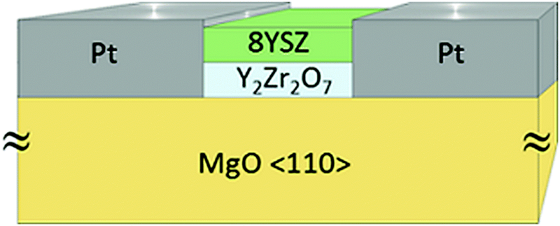 | ||
| Fig. 1 Illustration of the electrodes used to characterize the conductivity of multilayers of YSZ and Y2Zr2O7. | ||
The electrical properties were measured using an impedance spectrometer (Novocontrol Alpha-A High Performance Frequency Analyzer) operated at frequencies ranging between 2 MHz and 0.02 Hz by applying an A.C. voltage of 0.1 V. Impedance spectra were collected under oxidizing atmosphere; the pO2 was monitored by a commercial oxygen sensor (Rapidox 2100, Cambridge Sensotec). The resulting spectra were analyzed with the software Zview2 (Scribner Associates, Inc.).
The impedance spectra used for the determination of the electrical transport properties were acquired upon equilibration up to 40 hours at 500 °C and 8 hours at 700 °C at constant oxygen partial pressure while multilayers were exposed to a maximum temperature of 600 °C. For the analysis of EIS spectra of thin films, the capacitance of the films was not considered, since the parasitic capacitance deriving from the measurement set up and from the substrate typically overshades the film capacitance. Therefore, for the calculation of the electrical conductivity only the resistance determined by the spectra fit was used.
Results and discussion
Structural characterization
Single films of various thicknesses were deposited on Al2O3(0001), Al2O3(102) and MgO(110) while heterostructures consisting of alternating YSZ/Y2Zr2O7 layers were grown on MgO(110) only. The XRD patterns (Fig. 2a and b) show that Y2Zr2O7 films are mainly oriented along the (111) direction on Al2O3(102) as well as on Al2O3(0001). Peaks from the sample holder were not always present in the measurement and were dependent on the offset used. XRD patterns of thin film grown on Al2O3(102) were acquired after deposition of the electrodes, therefore also peaks stemming from platinum electrodes are visible.
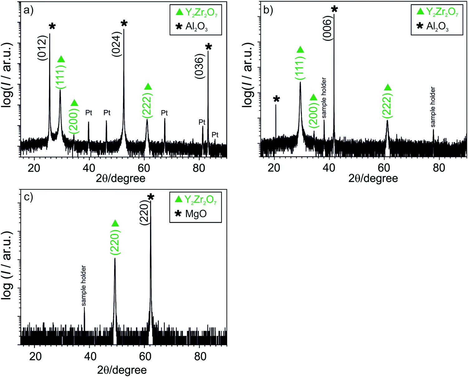 | ||
| Fig. 2 XRD patterns of Y2Zr2O7 thin films grown on (a) Al2O3(102), (b) Al2O3(0001), (c) MgO(110). | ||
In some samples a second weak peak corresponding to the (200) orientation has been observed. For the samples grown on MgO(110) (Fig. 2c) only the orientation (220) can be detected while the corresponding pole figures exhibit only two peaks at ψ = 45°, indicating perfectly epitaxial thin films (Fig. 3a). It is interesting to note that the films grown on the alumina substrates exhibit peaks belonging to two different orientations despite their smaller mismatch compared to MgO(110) (ranging between 10% and 15% on the two different Al2O3 substrates and amounting −23% on MgO). The result is consistent with the pole figures measurement, where the two distributed intensity along the ϕ axis, at ψ = 54°, indicate a textured in-plane alignment of the grains (Fig. 3b). The peaks are repeated every 120° along φ according to the threefold symmetry of the (111) plane. The intensity at ψ = 38° instead does not originate from the Y2Zr2O7 phase but from to the (104) plane of the substrate. The less intense signals visible in the pole figures are instead attributed to the background. AFM analysis of the film surfaces (not shown here) allowed for the determination of a very low surface roughness, comparable to the size of a unit cell for both the textured and the epitaxial samples (4.65–5.21 Å).
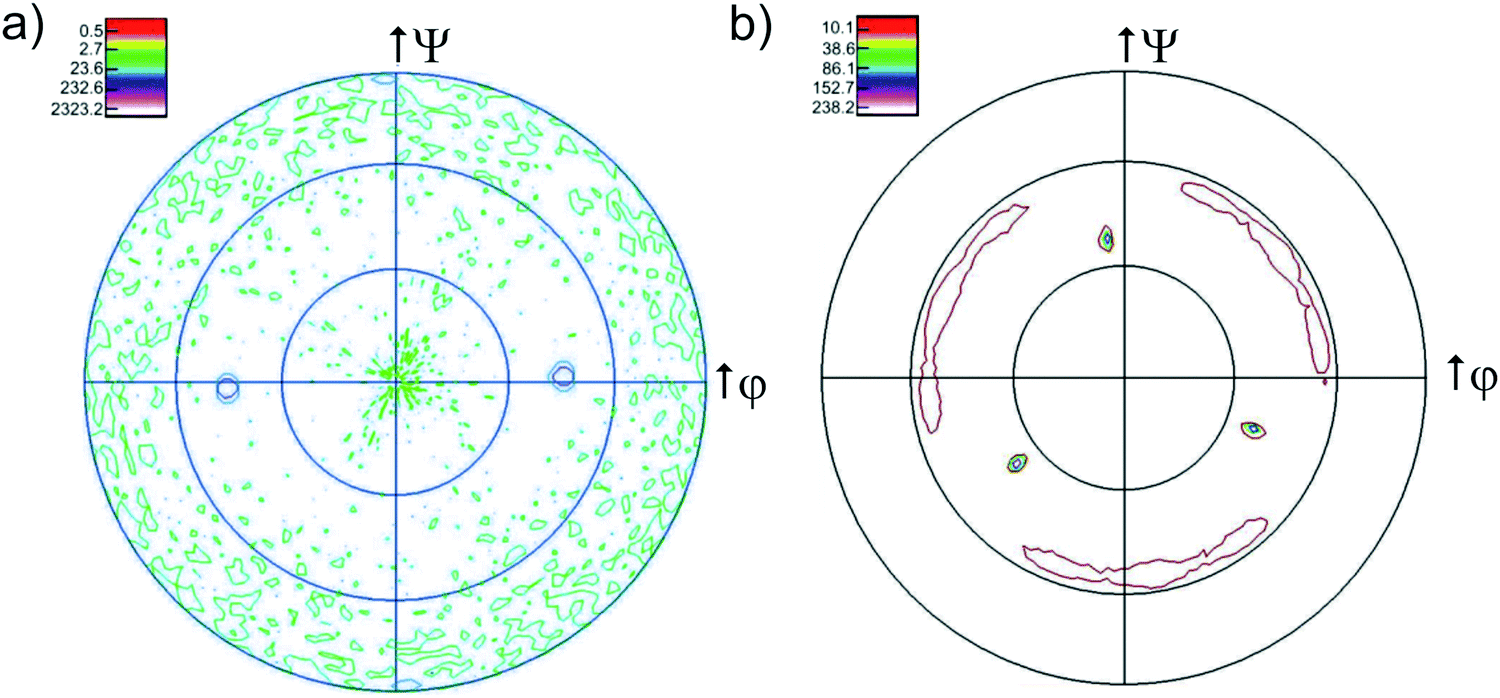 | ||
| Fig. 3 {001} Pole figure (2θCo-Kα = 40.5°) of (a) epitaxial thin film on MgO(110). (b) A textured thin film grown on Al2O3(0001): the distributed intensity along φ indicates the partially textured microstructure of the sample. | ||
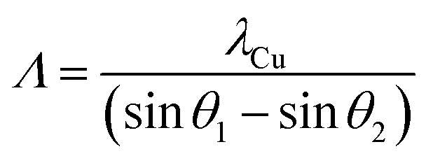
As far as the heterostructures are regarded, the XRD analysis (Fig. 4) reveals two peaks for the bilayer, while for the other heterostructures, the peaks are split in first order satellites peaks (labelled as SL1 and SL−1), which results from interference effects due to the high density of interfaces. As the angular spacing of the satellites peaks depends on the thickness of the layers referring for both the YSZ and Y2Zr2O7 layers to the same order peak, one can write37
 | (1) |
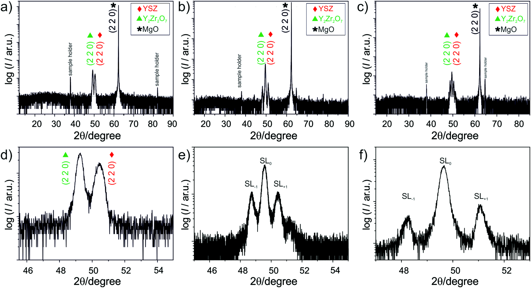 | ||
| Fig. 4 XRD patterns of YSZ/Y2Zr2O7 epitaxial heterostructures on MgO(110) having roughly the same overall thickness but different number of interfaces: 1 for (a), 5 for (b) and 10 for (c). In panels (d)–(f) the magnification of the corresponding reflections showing the additional peaks due to the interfaces are displayed. The satellites peaks SL1 and SL−1 allow for the calculation of the constituting unit (a single pair of YSZ and Y2Zr2O7 layers) thickness: 11.8 nm from (e) (5 × (10 nm–10 nm)) and 6.8 nm from (f) (10 × (5 nm–5 nm)). | ||
Reciprocal space maps on single layers and multilayers were obtained around the YSZ(331), (33), (420) and (240) reflections (Fig. 5). The in plane and out of plane momentum transfers can be separated considering that the reflection (420) is constituted by the sum of the vectors (330) and (10); while the (331) is the sum of (330) and (001) vectors.
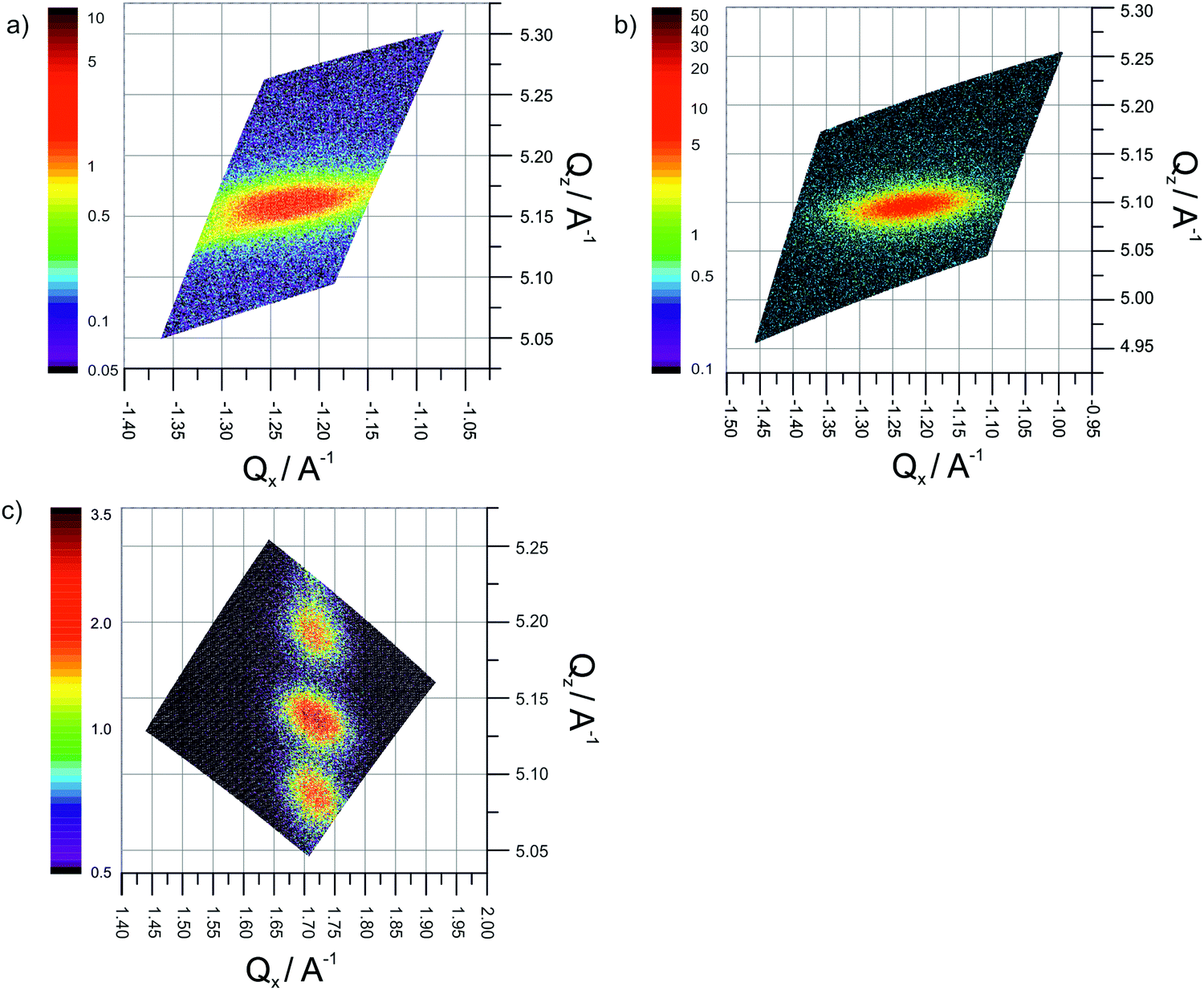 | ||
| Fig. 5 Reciprocal space maps around the (33-1) reflection of (a) single layer of Y2Zr2O7, (b) single layer of YSZ. Reciprocal space map around the (420) reflection of a multilayer 5 × (10 nm + 10 nm), which were all grown epitaxially on MgO(110). Qx and Qz indicate the in plane and out of plane momentum transfer respectively. Color indicates the intensity (in arbitrary units). The intensity is reported in logarithmic scale in (a) and (b) and in linear scale in (c). | ||
In Fig. 5a and b are shown the reciprocal space maps around the reflections (33), of a single layer of Y2Zr2O7 (70 nm thickness) and a single layer (60 nm thickness) of YSZ respectively, all grown epitaxially on MgO(110). The elongated shape of peak along the in plane momentum transfer direction is related to the presence of defects in the sample. Since the TEM analysis (reported in ref. 36 for a Y2Zr2O7 single layer) confirmed the absence of grain boundaries or mosaic microstructure, such effect is attributed to the high density of misfit dislocations at the interface.
Both the in-plane Qx and out-of-plane Qz momentum transfers show an almost complete relaxation of the strain deriving from the mismatch with the substrate. Notably, for the YSZ thin film, the comparison with the values of interplanar distance reported in literature (ICDD: 01-082-1246) reveal an out-of-plane value along the [110] direction of +0.5%, while in plane an average (compressive) strain of −0.9% is found. Such an outcome is qualitatively expected since it corresponds to the situation, according to which the substrate MgO(110) having a smaller lattice parameter keeps the film under in-plane compressive strain. Such an in-plane compression demands an expansion in the perpendicular direction in agreement with expected Poisson ratio.
A similar situation (although to a different extent) holds also for the Y2Zr2O7 thin film. Here, the in-plane compressive strain is equal to −0.4%, while along out-of-plane direction the strain is 0.3%.
The reciprocal space map around the (420) reflection of the 5 × (10 nm + 10 nm) multilayer (Fig. 5c) clearly exhibits satellite peaks stemming from the periodicity of the system. In this case, it is not possible to separate YSZ and Y2Zr2O7 in-plane contributions, due to the very similar lattice parameters of the two materials. Nonetheless, the out-of-plane lattice parameters could be estimated by simulating the intensity profile of a stack of ([YSZ]20[YZO]20)5. This indicates an out-of-plane lattice expansion of +0.4% suggesting that also the multilayers are kept under in-plane compressive strain by the substrate as observed in the single layers.
Also in this case the broadening of the peaks can be attributed to a high density of extended defects perpendicular to the interface, most likely misfit dislocations at the interface to the substrate. In this context, the Scherrer's formula cannot be directly used to calculate the average distance between the dislocations since the peak broadening depends also on the intensity of the Burgers’ vector of the dislocation and the relative orientation of between the Burgers vector and line dislocation.39 Nevertheless the difference in the peak broadening between the single layers suggests a different density of misfit dislocation in the samples. In particular, it indicates a larger misfit density in the single layer of YSZ compared to the Y2Zr2O7 single layer and the multilayers.
Electrical measurements
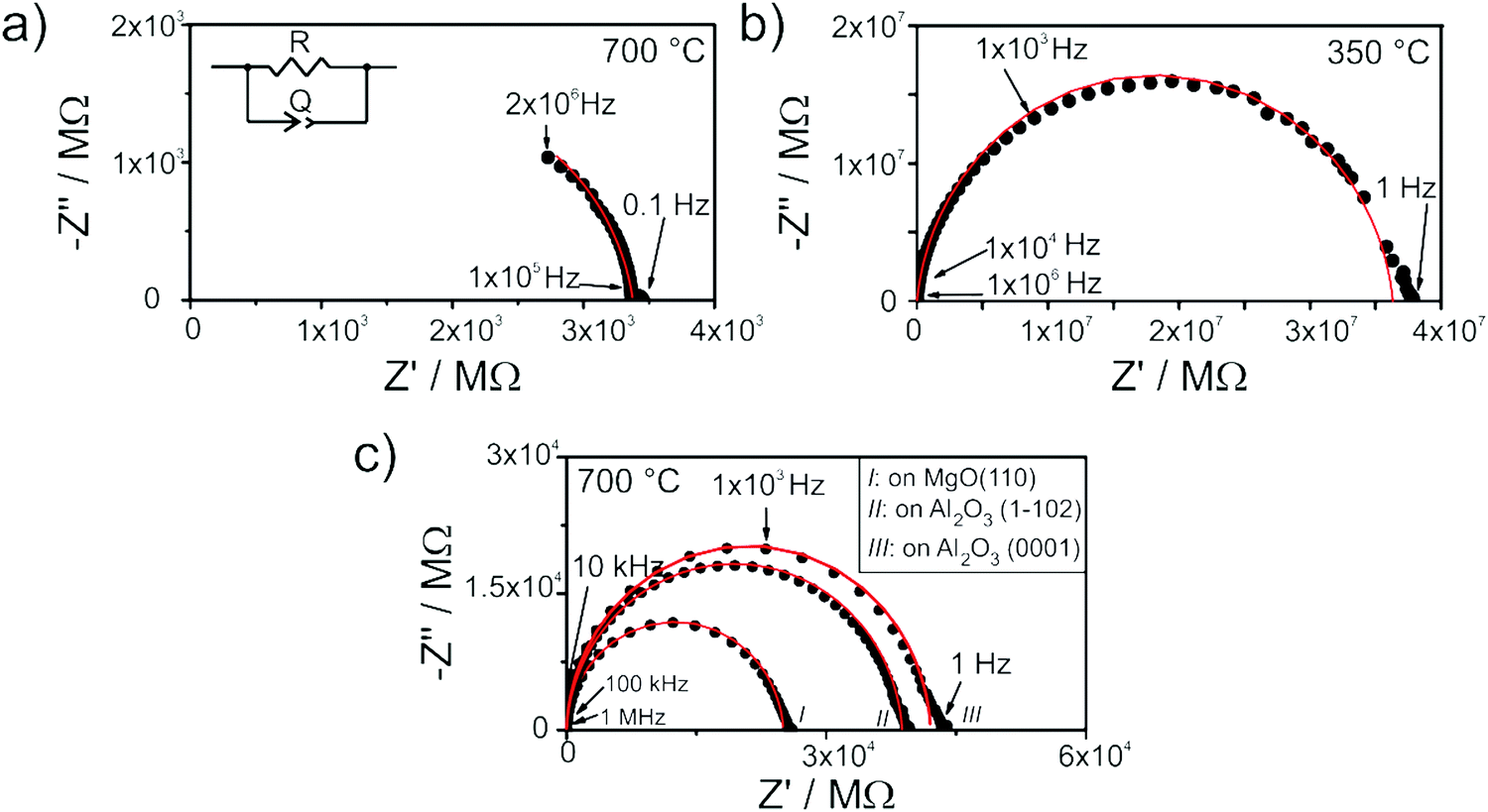 | ||
| Fig. 6 Impedance Nyquist plot of (a) a microcrystalline pellet acquired in oxygen at 700 °C (b) of the same sample at 350 °C, (c) of thin films 100 nm thick grown on different. The symbols correspond to the experimental data while the continuous lines result from fitting the spectra using the equivalent circuit in the inset of (a). | ||
Also the spectra acquired from the single thin films (Fig. 6b and c) exhibit only one semicircle. This is expected as, owing to the experimental setup configuration, the resulting stray capacitance exceeds the bulk and grain boundary capacitances by orders of magnitude.40 For this reason, it is not possible to distinguish bulk from grain boundary contribution, and the impedance spectra are fitted using the same equivalent circuit as the one shown above.
The resulting electrical conductivity and activation energy data are summarized in Fig. 7 and Table 1. It is evident that not only textured and epitaxial films (Fig. 7a) but also epitaxial and polycrystalline samples (Fig. 7b) exhibit very similar electrical conduction properties suggesting that the microstructure (i.e. the presence of grain boundaries) only marginally affects the ionic transport. It is worth comparing these results with literature data obtained from YSZ thin films. For example, Peters et al.41 observed variation of one order of magnitude in the conductivity of Y0.17Zr0.83O1.91 thin films (from 10−2 S cm−1 to 10−3 S cm−1 at 700 °C) by varying the grain size from about 40 nm to 150 nm in 400 nm thick layers deposited by sol–gel method. Similarly, Schlupp et al.42 measured a conductivity decrease of more than 1 order of magnitude (from 8 × 10⁻⁵ S cm−1 to 1 × 10⁻⁶ S cm−1 at 400 °C), together with an activation energy increase of 0.3 eV when comprising columnar grown with nanocrystalline thin films of 8YSZ deposited via chemical vapor deposition.
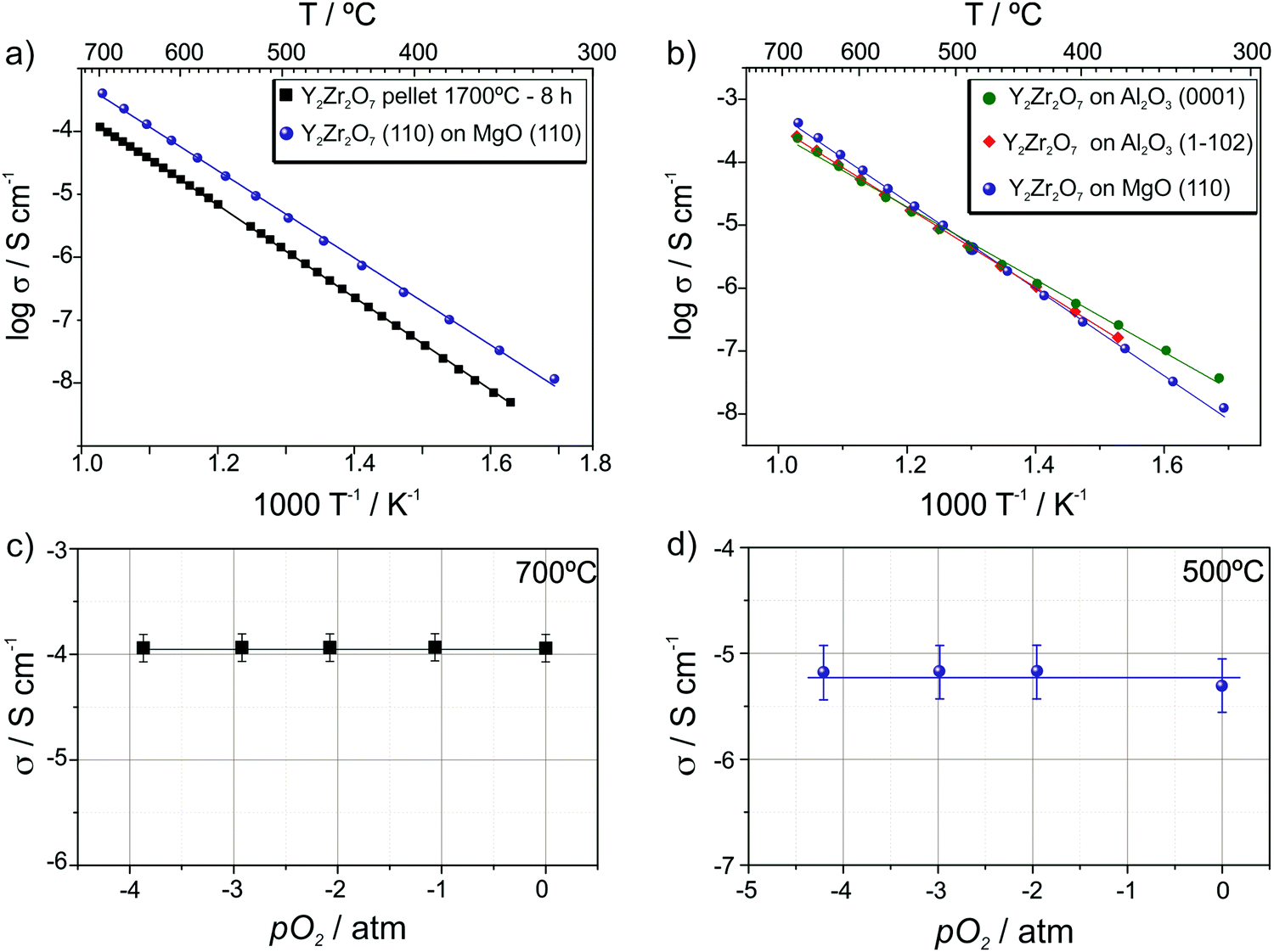 | ||
| Fig. 7 Temperature dependence and activation energy of (a) Y2Zr2O7 pellet compared with an epitaxial thin film grown on MgO, (b) Y2Zr2O7 thin films on different substrates, MgO and Al2O3, constant thickness 100 nm. pO2 dependence of the conductivity of (c) a ceramic pellet and (d) of an epitaxial thin film on MgO. | ||
| Y2Zr2O7 sample | Activation energy/eV | σ at 700 °C/S cm−1 |
|---|---|---|
| On MgO(110) epitaxial | 1.44 ± 0.01 | 4.01 × 10⁻⁴ |
| On Al2O3(0001) textured | 1.26 ± 0.01 | 2.37 × 10⁻⁴ |
| On Al2O3(102) textured |
1.32 ± 0.01 | 2.58 × 10⁻⁴ |
| Pellet | 1.52 ± 0.002 | 1.17 × 10⁻⁴ |
These results allow one to conclude that compared to a parent system (8YSZ), the grain boundaries in Y2Zr2O7 do not hinder the oxygen vacancy transport. To the best of our knowledge there are no studies about grain boundary contribution to the ionic conductivity in zirconate pyrochlores or defective fluorite thin films in the literature whereas a markedly blocking effect of the grain boundaries has been noticed in pyrochlore ceramics with the composition (Sm1−xYx)2Zr2O7 with 0 ≤ x ≤ 0.543 and GdSmZr2O7.44
We note that as expected for a defective fluorite, both the films and the pellet do not show any conductivity dependence on the oxygen partial pressure in the range between 1 and 10−4 atm at 700 °C (cf.Fig. 7c and d).
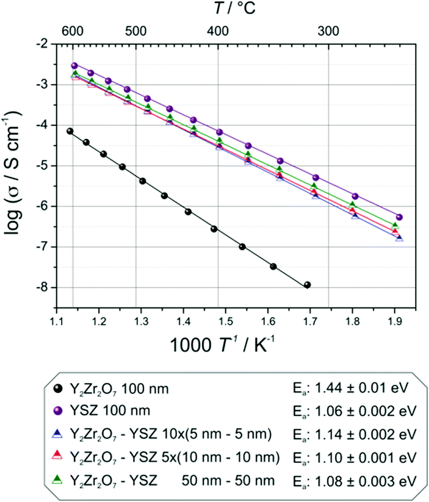 | ||
| Fig. 8 Temperature dependence of the conductivity of YSZ–Y2Zr2O7 multilayers with different number of interfaces. For comparison also the data of single layers of YSZ and Y2Zr2O7 are displayed. | ||
It is noteworthy that the conductivity and activation energy values for the single layer of YSZ are in agreement with literature values: Joo et al.45 reported a conductivity of 3 × 10⁻³ S cm−1 at 600 °C, in this work the measured conductivity is 2.9 × 10⁻³ S cm−1 and an activation energy of 1.01 eV for a YSZ PLD-film of 0.6 μm thickness.
In absence of interface effects (e.g. space-charge or strain), the multilayer systems considered here can be treated as a set of resistances in parallel, each of which corresponding to a single layer. The expected total conductivities can be calculated according to Kirchoff's law starting from the conductivities of the constituting oxides. In this way, we estimate a conductivity of the multilayers of 1.5 × 10⁻³ S cm−1 at 600 °C.
The actual experimental values measured at 600 °C are: 1.7 × 10⁻³ S cm−1 for the 10 × (5–5) multilayer, 1.5 × 10⁻³ S cm−1 for the 5 × (10–10) multilayer and 1.8 × 10⁻³ S cm−1 for the bilayer. Such a small difference between the expected and the measured values indicates that the conductivity of the heterolayers is neither varied by the number of interfaces nor by the different thicknesses of the single constituting layers, meaning that neither space charge nor strain effects modify the ion transport properties compared to the bulk situation. Consistently, also the values of the activation energy vary only marginally (from 1.08 eV for the bilayer to 1.10 eV for the 5 × (10–10) and 1.14 eV for the 10 × (5–5) samples).
From thermodynamic considerations, it has been calculated that the strain alters the ionic transport and its effect is proportional to the mismatch between layers (this is strictly valid only for epitaxial systems).27 Here, however we recognize that even in perfectly epitaxial systems with high quality of the interfaces (confirmed by XRD analysis) below the critical thickness, where the strain is not released through one-dimensional or two-dimensional defects, the substantial residual strain field (compressive in-plane and tensile out-of-plane) does not result in any perceptible variation of the oxygen ion transport.
To the best of our knowledge, there are no theoretical studies in literature on the effect of compressive strain on the ionic conductivity of YSZ. Nonetheless if we refer to studies on the effect of tensile strain on the ionic transport of YSZ (as the work by Kushima and Yildiz25) and assume a symmetric effect in the case of a compressive strain, our results are in qualitative agreement with the literature. The authors reported an increasing effect of the strain on the hopping barrier of oxygen vacancies up to a strain of 4% with such an effect being more pronounced at lower temperatures. It is worth noticing that, not only the trend of an increasing effect on the activation energies with increasing strain is in agreement with our observation, but also the variation of the activation energy (calculated for less than 1% strain) being close to 0.1 eV is consistent with our experimental findings.
For the sake of completeness, we note that our results are however not in line with the observations of Li et al.,29 who detected a different behavior for their multilayered Gd2Zr2O7 and YSZ heterostructures grown on Al2O3 with a variable number of interfaces. In that study, the authors measured a substantial variation of the ionic conductivity (an increase of 2 orders of magnitude when moving from 10 to 20 interfaces) for a lattice mismatch of about 3%, while no information was given on the activation energy. It is arduous to rationalize such a discrepancy, since it might well depend on different procedures of the sample preparation that might lead to nominally similar samples but having different microstructures and/or strain situations. In this work, we took carefully into account the microstructure and real residual strain of the multilayers, observing that secondary effects stemming from grain boundaries and misfit dislocations can be excluded to be present in our multilayered samples.
Conclusions
Y2Zr2O7 thin films have been successfully grown on various substrates (MgO(110), Al2O3(0001), Al2O3(102)) by pulsed laser deposition. The study of their electrical properties (impedance spectroscopy) at different temperatures and oxygen partial pressure shows that these are only marginally affected by their orientation and microstructure, since the ionic conductivity variation amounts only a factor two between epitaxial (on MgO(110)) and polycrystalline thin films (on Al2O3(0001) and Al2O3(102)).
Heterolayers of YSZ/Y2Zr2O7 with different number of interfaces were characterized to investigate the role of strain on the ionic conductivity of YSZ. A combined study relying on the determination of the residual strain field in the multilayers and on the evaluation of their ionic transport properties did not reveal any perceptible effect of strain on the oxygen vacancy transport. Such a finding may be interpreted in term of a mutually compensating effect between the deleterious compressive in-plane strain and the beneficial tensile out-of-plane strain resulting from the substrate MgO(110) with a smaller lattice constant compared to YSZ and Y2Zr2O7.
Author contributions
The manuscript was written through contributions of all authors. All authors have given approval to the final version of the manuscript.Conflicts of interest
There are no conflicts to declare.Acknowledgements
The authors wish to thank G. Christiani and B. Stuhlhofer for their technical support for pulsed laser deposition. R. Merkle is thanked for helpful discussions. M. Dudek is thanked for the pole figure acquisition. H. Boschker is thanked for the RSM characterization. Fig. 2c, 3a, and 7a were adapted with permission from (ACS Appl. Mater. Interfaces, 9(32), 27257–27265). Copyright (2017) American Chemical Society. Open Access funding provided by the Max Planck Society.References
- E. Fabbri, D. Pergolesi and E. Traversa, Sci. Technol. Adv. Mater., 2010, 11, 054503 CrossRef PubMed.
- X. Guo and J. Maier, Adv. Mater., 2009, 21, 2619–2631 CrossRef.
- X. Guo and J. Maier, J. Electrochem. Soc., 2001, 148, E121–E126 CrossRef.
- C. Peters, A. Weber, B. Butz, D. Gerthsen and E. Ivers-Tiffée, J. Am. Ceram. Soc., 2009, 92, 2017–2024 CrossRef.
- M. C. Gobel, G. Gregori and J. Maier, Phys. Chem. Chem. Phys., 2011, 13, 10940–10945 RSC.
- S. Kim, J. Fleig and J. Maier, Phys. Chem. Chem. Phys., 2003, 5, 2268–2273 RSC.
- Y. M. Chiang, E. B. Lavik, I. Kosacki, H. L. Tuller and J. Y. Ying, Appl. Phys. Lett., 1996, 69, 185–187 CrossRef.
- X. Guo and R. Waser, Prog. Mater. Sci., 2006, 51, 151–210 CrossRef.
- W. J. Bowman, M. N. Kelly, G. S. Rohrer, C. A. Hernandez and P. A. Crozier, Nanoscale, 2017, 9, 17293–17302 RSC.
- C. T. Chen, S. Sen and S. Kim, Chem. Mater., 2012, 24, 3604–3609 CrossRef.
- J. T. S. Irvine, I. R. Gibson and D. P. Fagg, Ionics, 1995, 1, 279–285 CrossRef.
- N. Shibata, F. Oba, T. Yamamoto, Y. Ikuhara and T. Sakuma, Philos. Mag. Lett., 2002, 82, 393–400 CrossRef.
- H. B. Lee, F. B. Prinz and W. Cai, Acta Mater., 2013, 61, 3872–3887 CrossRef.
- M. C. Gobel, G. Gregori and J. Maier, Phys. Chem. Chem. Phys., 2014, 16, 10214–10231 RSC.
- D. S. Mebane and R. A. De Souza, Energy Environ. Sci., 2015, 8, 2935–2940 RSC.
- J. L. M. Rupp, Solid State Ionics, 2012, 207, 1–13 CrossRef.
- N. Schichtel, C. Korte, D. Hesse and J. Janek, Phys. Chem. Chem. Phys., 2009, 11, 3043–3048 RSC.
- N. Sata, K. Eberman, K. Eberl and J. Maier, Nature, 2000, 408, 946–949 CrossRef PubMed.
- G. Xiangxin, I. Matei, J. Jamnik, L. Jong-Sook and J. Maier, Phys. Rev. B: Condens. Matter Mater. Phys., 2007, 76, 1–7 Search PubMed.
- R. A. De Souza, A. Ramadan and S. Horner, Energy Environ. Sci., 2012, 5, 5445–5453 RSC.
- A. P. C. Korte, J. Janek, D. Hesse and N. Zakharovb, Phys. Chem. Chem. Phys., 2008, 10, 4623–4635 RSC.
- C. Korte, N. Schichtel, D. Hesse and J. Janek, Monatsh. Chem., 2009, 140, 1069–1080 CrossRef PubMed.
- J. Hinterberg, T. Zacherle and R. A. De Souza, Phys. Rev. Lett., 2013, 110, 205901 CrossRef PubMed.
- N. Schichtel, C. Korte, D. Hesse, N. Zakharov, B. Butz, D. Gerthsen and J. Janek, Phys. Chem. Chem. Phys., 2010, 12, 14596–14608 RSC.
- A. Kushima and B. Yildiz, J. Mater. Chem., 2010, 20, 4809–4819 RSC.
- D. S. Aidhy, Y. W. Zhang and W. J. Weber, J. Phys. Chem. C, 2014, 118, 4207–4212 CrossRef.
- C. Korte, J. Keppner, A. Peters, N. Schichtel, H. Aydin and J. Janek, Phys. Chem. Chem. Phys., 2014, 16, 24575–24591 RSC.
- B. Yildiz, MRS Bull., 2014, 39, 147–156 CrossRef.
- B. Li, J. M. Zhang, T. Kaspar, V. Shutthanandan, R. C. Ewing and J. Lian, Phys. Chem. Chem. Phys., 2013, 15, 1296–1301 RSC.
- D. Pergolesi, E. Fabbri, S. N. Cook, V. Roddatis, E. Traversa and J. A. Kilner, ACS Nano, 2012, 6, 10524–10534 CrossRef PubMed.
- A. Fluri, D. Pergolesi, V. Roddatis, A. Wokaun and T. Lippert, Nat. Commun., 2016, 7, 10692 CrossRef PubMed.
- W. D. Shen and J. L. Hertz, J. Mater. Chem. A, 2015, 3, 2378–2386 RSC.
- L. Minervini, R. W. Grimes and K. E. Sickafus, J. Am. Ceram. Soc., 2000, 83, 1873–1878 CrossRef.
- B. P. Uberuaga, D. A. Andersson and C. R. Stanek, Curr. Opin. Solid State Mater. Sci., 2013, 17, 249–256 CrossRef.
- T. Hagiwara, H. Yamamura and H. Nishino, J. Fuel Cell Sci. Technol., 2011, 8, 1–5 CrossRef.
- E. Gilardi, G. Gregori, Y. Wang, W. Sigle, P. A. van Aken and J. Maier, ACS Appl. Mater. Interfaces, 2017, 9, 27257–27265 CrossRef PubMed.
- S. Sanna, V. Esposito, A. Tebano, S. Licoccia, E. Traversa and G. Balestrino, Small, 2010, 6, 1863–1867 CrossRef PubMed.
- M. M. Hall, V. G. Veeraraghavan, H. Rubin and P. G. Winchell, J. Appl. Crystallogr., 1977, 10, 66–68 CrossRef.
- C. C. Tang, J. Appl. Crystallogr., 2007, 40, 642–649 CrossRef.
- M. Gerstl, E. Navickas, M. Leitgeb, G. Friedbacher, F. Kubel and J. Fleig, Solid State Ionics, 2012, 225, 732–736 CrossRef PubMed.
- C. Peters, A. Weber, B. Butz, D. Gerthsen and E. Ivers-Tiffee, J. Am. Ceram. Soc., 2009, 92, 2017–2024 CrossRef.
- M. V. F. Schlupp, B. Scherrer, H. Ma, J. G. Grolig, J. Martynczuk, M. Prestat and L. J. Gauckler, Phys. Status Solidi A, 2012, 209, 1414–1422 CrossRef.
- X. L. Xia, J. H. Ouyang, Z. G. Liu, S. A. Gao and S. Li, J. Electrochem. Soc., 2010, 157, B470–B476 CrossRef.
- Z. G. Liu, J. H. Ouyang, K. N. Sun and Y. Zhou, J. Power Sources, 2012, 210, 96–100 CrossRef.
- J. H. Joo and G. M. Choi, Solid State Ionics, 2006, 177, 1053–1057 CrossRef.
Footnote |
| † Present address: Laboratory for Multiscale Materials Experiments, Paul Scherrer Institut, 5232 Villigen, Switzerland. |
| This journal is © the Owner Societies 2018 |