
 Open Access Article
 This Open Access Article is licensed under a
 Creative Commons Attribution 3.0 Unported Licence
Organometallic MTCNQ films: a comparative study of CuTCNQ versus AgTCNQ
Maria J.
Capitán
 *ab,
Jesus
Alvarez
bc and
Felix
Yndurain
c
*ab,
Jesus
Alvarez
bc and
Felix
Yndurain
c
aInstituto de Estructura de la Materia, CSIC, c/Serrano 119, 28006 Madrid, Spain. E-mail: mj.capitan@csic.es
bGrupo Física de sistemas crecidos con baja dimensionalidad, UAM, unidad asociada a IEM-CSIC, Spain
cDpto. Fisica Materia Condensada and the Condensed Matter Physics Center (IFIMAC)-Instituto Nicolas Cabrera, UAM, Facultad de Ciencias, CIII. Ctra. Colmenar Viejo km 14.5, 28049, Madrid, Spain
First published on 13th August 2018
Abstract
We performed a systematic study of electron-acceptor molecules in two closely related organometallic solids, namely, CuTCNQ and AgTCNQ. These studies were performed using both an experimental approach, via the use of electron spectroscopies (XPS and UPS), and a theoretical approach, via the use of ab initio DFT calculations. From these results, a complete description of the electronic structure of these molecular solid-films could be given, identifying the characteristic electronic and structural features of each part of the molecules and their contribution to the final electronic structure. Empty states were found close to the Fermi level in both solids. The presence of an electronic band close to the Fermi level is related to the magnetic behavior predicted for both MTCNQ solids for their isolated monolayers. However, the lower work function of the MTCNQ with respect to the metal substrate one implies that the MTCNQ film accepts electron from the metal substrate, thus fulfilling its Fermi level band. This occupied band explains the absence of shake-up features in the core level spectra in opposition to the TCNQ. The UPS experiments indicated that the MTCNQ film was doped by a small excess of metal from the substrate, shifting the electron Fermi level close to the MTCNQ conduction band. Thus, the MTCNQ film becomes an n-type semiconductor, opening up a very interesting field in the technological applications of this system.
I. Introduction
Organic electronic devices are gaining greater prominence among commercial electronic devices in such a rapid way that, with their current fast evolution, electronics based on this technology will be soon be part of our daily use technology. In fact, products based on active thin-film organic devices are already in the market place.1 These devices have found their way into many applications, such as diodes,2 transistors, photodetectors,3 and memory cells.4 One of the most notable applications is their use in the displays of several mobile electronic appliances. These systems are being developed against the backdrop of today's conventional and large-area electronics technologies, where the dominant semiconductor is silicon in single crystalline, polycrystalline, or amorphous forms.Many organic conductors are based on flat molecules, which can pile up into linear stacks, with conduction taking place along the direction of the stack.5 Among these molecules, the archetype of these conductors is the 7,7,8,8-tetracyanoquinodimethane family (TCNQ). The conduction mechanism in TCNQs is based on charge injection in the lowest unoccupied molecular orbital (LUMO), which can accept electrons from metals or other molecules.6 Therefore, the TCNQ molecule is a well-known strong electron-acceptor that forms part of a rich variety of charge-transfer materials with various metals. The metal salts of TCNQ behave as charge-transfer complexes and show a wide range of interesting electronic, optical, and magnetic effects, making these organometallic electron-acceptor molecules very suitable for use in many technological applications. However, most of the revealed properties shown in the literature to date lack reports on the correlation between them and the physics and chemistry underlying these properties. An overall vision between them is still lacking. In this article, we report such systematic research with an aim to correlate all the electronic properties and to answer all the issues arising from the study of the electronic properties of such films and their interface with a metal surface in two TCNQ-salts, namely CuTCNQ and AgTCNQ.
Both the TCNQ-salts, CuTCNQ and AgTCNQ, are semiconductors with switching electrical behavior, which could make these compounds ideal for use in organic electronic applications.7,8 However, the nature of the switching mechanism is not yet clear. Some authors claim that it is related with a bulk-related phenomenon,7,9,10 while other authors report that the switch effect is located at the interface.11,12 Therefore, understanding their crystal and electronic structures in the bulk and at the interface with a substrate is crucial for the design and development of electronic devices based on these materials.
CuTCNQ has two phases with different physical properties, but it is the semiconductor phase-I13 that shows this switching behavior, and therefore this is the ideal phase for organic electronics applications.7 CuTCNQ has been synthesized following several reaction paths that vary from electrochemical methods,14 solid–liquid-phase reaction,15 solid–gas reaction,11 and vacuum codeposition.7 In most of these methods, the homogeneity, crystallinity, and grain orientation cannot be controlled in a satisfactory way, which makes their use for thin-film applications difficult. However, it has been proposed that CuTCNQ can be grown by a solid-phase reaction, in which Cu diffuses on to a TCNQ layer deposited on Cu substrates.16 In the case of growing CuTCNQ by a solid-phase reaction, it is crucial to control the growth mode, structure, and morphology of the former TCNQ film acting as a precursor for the cooper reaction and diffusion. We have shown in previous work16,17 that the growth of TCNQ films on bare substrates can form very crystalline and oriented films by evaporating TCNQ molecules under UHV conditions at a low evaporation rate and low substrate temperature. The crystallinity of the TCNQ layers grown on Cu substrates is of great importance in order to grow well-ordered CuTCNQ films by a solid-phase reaction.
In this work, we grew semiconducting MTCNQ films by diffusing metal atoms from the substrate to form a well-ordered semiconductor film so that we could perform a systematic study of the electronic properties of MTCNQ films grown on a metal substrate with a clean and well controlled interface. For this purpose, we studied the MTCNQ film growth on a metal surface by studying the changes in the electronic structure, and we compared the results for two different metals (Cu and Ag) as a cross-check of these properties in order to undoubtedly confirm our results and conclusions. Surface analysis techniques, such as X-ray photoelectron spectroscopy (XPS), ultraviolet photoelectron spectroscopy (UPS), and inverse photoemission (IPES) were used for the characterizations as they can give information about the Fermi level and the electronic structure of a material. We compared these results and those present in literature to our theoretical results. Here, we used first principles theoretical calculations performed in the context of density functional theory18,19 using the SIESTA20,21 code, which has largely demonstrated good performance for such large molecular solids.22 It is noticeable how few theoretical studies have been made on MTCNQ systems, with a particular absence of studies combining theoretical and experimental studies that could allow a cross-check of the electronic structures and their properties. This is especially surprising when we take into account the large technological interest in these systems in recent years and the number of still unanswered questions related to their exhibited electronic and magnetic properties.
II. Methods
TCNQ (7,7,8,8-tetracyanoquinodimethane) powder from Sigma Aldrich was used in the experiment. The TCNQ films were deposited on Cu(001) and on Ag(001) single crystals under ultrahigh vacuum (UHV) conditions, respectively. We prepared the Cu(001) and Ag(001) single crystals substrates by in situ Ar+ sputtering and flash-annealing cycles under UHV conditions with a base pressure of 2 × 10⁻¹⁰ mbar. As a result of this a sharp diffraction pattern could be observed, being even present with their surface diffraction rods. TCNQ was deposited by thermal evaporation from glass crucibles at a pressure of 1 × 10⁻⁸ mbar and 5 × 10⁻⁷ mbar. The growth rates for TCNQ were set from 0.8 ML per min (monolayer per min), which corresponded to a crucible temperature of 65 °C.At room temperature, the metal substrate diffuses through the TCNQ, becoming a MTCQ film, with M = Ag or Cu depending on the used substrate (see Fig. 1). The complete MTCNQ formation was confirmed structurally by in situ X-ray diffraction (XRD) measurements and chemically by numerical X-ray photoelectron spectroscopy (XPS) analysis. The XRD experiments were made at a fixed incidence angle of 2° performed at the W1.1 beamline at Hasylab synchrotron at Desy. This extended diffusion has already been reported elsewhere.16,23
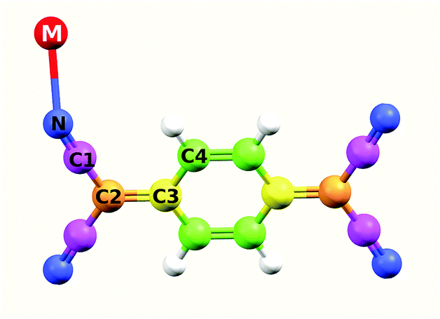 | ||
| Fig. 1 Sketch of the MTCNQ molecule. | ||
The electronic properties were studied with an XPS system with a monochromatic Al Kα line, a hemispherical energy analyzer (SPHERA-U7), and an ultraviolet He discharge lamp for ultraviolet photoelectron spectroscopy analysis for the valence band measurements (UPS), and low-energy electron diffraction (LEED) optics. The Al Kα line (hν = 1486.7 eV) was used for XPS and the He-I (hν = 21.2 eV) and He-II (hν = 40.8 eV) lines for the UPS measurements. The pass energy of the analyzer was set to 20 eV for the XPS measurements, in order to have a resolution of 0.6 eV; whereas for the UPS, the pass energy was set to 5 eV, corresponding to a resolution of 0.1 eV. All the core levels are herein referred to the Cu 2p3/2 core level of the substrate (binding energy of 932.3 eV) and the UPS spectra to the Fermi edge of the Cu substrate in the CuTCNQ and to the Ag 3d5/2 core level (binding energy of 367.9 eV) of the substrate in the AgTCNQ case.
In order to study the geometrical and electronic structure of both CuTCNQ and AgTCNQ films, we used first principles density functional18,19 calculations using the SIESTA code,20,21 which use localized orbitals as the basis functions.24 We used a double-ζ basis set (in some instances, the results were checked increasing the basis with polarized orbitals) and non-local norm conserving pseudopotentials; while for the exchange correlation functional, we used the generalized gradient approximation (GGA),25 including van der Waals interaction in the way implemented by Roman-Perez and Soler26 with the functional developed by Dion et al.27 The calculations were performed with stringent criteria in the electronic structure convergence (down to 10−5 in the density matrix), 2D Brillouin zone sampling (up to 600 k-points), a real space grid with an energy cut-off of 400 Ryd to avoid “eggbox” effects, and equilibrium geometry (residual forces lower than 2 × 10⁻² eV Å−1). Due to the rapid variation of the density of states at the Fermi level, we used a polynomial smearing method.28 The calculated results were compared to the experimental valence band photoemission measurements (see below).
III. Results and discussion
I. The MTCNQ structure
In this work, we grew MTCNQ films by diffusing metal–substrate atoms through a former well-ordered and very oriented TCNQ film grown on a metal single-crystal substrate. This method was used because it produces organometallic MTCNQ films with a very ordered and controlled structure.16 The initial very well-crystallized and very oriented TCNQ film was grown by evaporating TCNQ molecules under UHV conditions and a controlled low substrate temperature (t = −50 °C). The cool TCNQ film had a monoclinic lattice29,30 with the TCNQ c-axis lying normal to the substrate surface direction.17 When the TCNQ film was set at room temperature, the metal–substrate atoms diffuse along the whole film thickness, resulting in the formation of an organometallic MTCNQ film, with M = Cu or Ag depending on the used substrate (Cu(001) or Ag(001), respectively). The result was a very well-ordered and highly oriented film, comprised the stacked MTCNQ c-axis perpendicular to the substrate (001) surface in both cases (Cu and Ag). In this orientation, the metal-containing planes are parallel to the substrate surface and the organic TCNQ molecules show a double herringbone structure perpendicular to the substrate surface direction (see Fig. 3 where the difference between the MTCNQ film with the former TCNQ-film structure, which is characterized by a single herringbone structure in the perpendicular to the substrate direction, can be observed). In both cases, the metal atom diffusion is complete along the initial TCNQ film, and no traces of this initial TCNQ structure can be found.Parallel to the substrate surface, the AgTCNQ, which has an orthorhombic 3D lattice, has an in-plane lattice with a = 16.686 Å and b = 17.455 Å and α = β = 90°.31 In the CuTCNQ films, our X-ray diffraction measurements fitted with an in-plane lattice with the lattice equal to a = 15.83 Å, and b = 15.93 Å and α = β = 90°, indicating a lattice slightly lower than the AgTCNQ, corresponding to a smaller metal atom.16 This structure is compatible with the structure given by Heintz et al. 1999,13 for the phase-I CuTCNQ, if a larger reducible lattice is taken. These authors gave a lattice of a = b = 11.266 Å and α = β = 90° for CuTCNQ. If we take the a and the b parameters √2 larger and 45° rotated around the c-axis (see Fig. 2A) in the lattice given by Heintz et al.,13 it results in an orthorhombic lattice with ar = br = 15.933 Å and α = β = 90° (the r index indicates that they are reducible parameters). With this lattice, both the AgTCNQ and CuTCNQ structures are very similar, showing this representation is better to compare both MTCNQ structures. A double cross-check between the experimental X-ray diffraction structure and the theoretical optimized structure was for the solids shown herewith. In Fig. 2B, we show the dependence of the theoretical system energy versus the a,b-lattice parameter in the CuTCNQ case. It can be observed that the resulting dependence gives a very flat minimum energy at a lattice parameter of around 16.3 Å. The curve is especially flat when we compare the relative energy change with the total energy of the system, which was around 15![[thin space (1/6-em)]](https://www.rsc.org/images/entities/char_2009.gif) 000 eV. In this calculation, we used the approach that a = b in order to simplify the calculation.
000 eV. In this calculation, we used the approach that a = b in order to simplify the calculation.
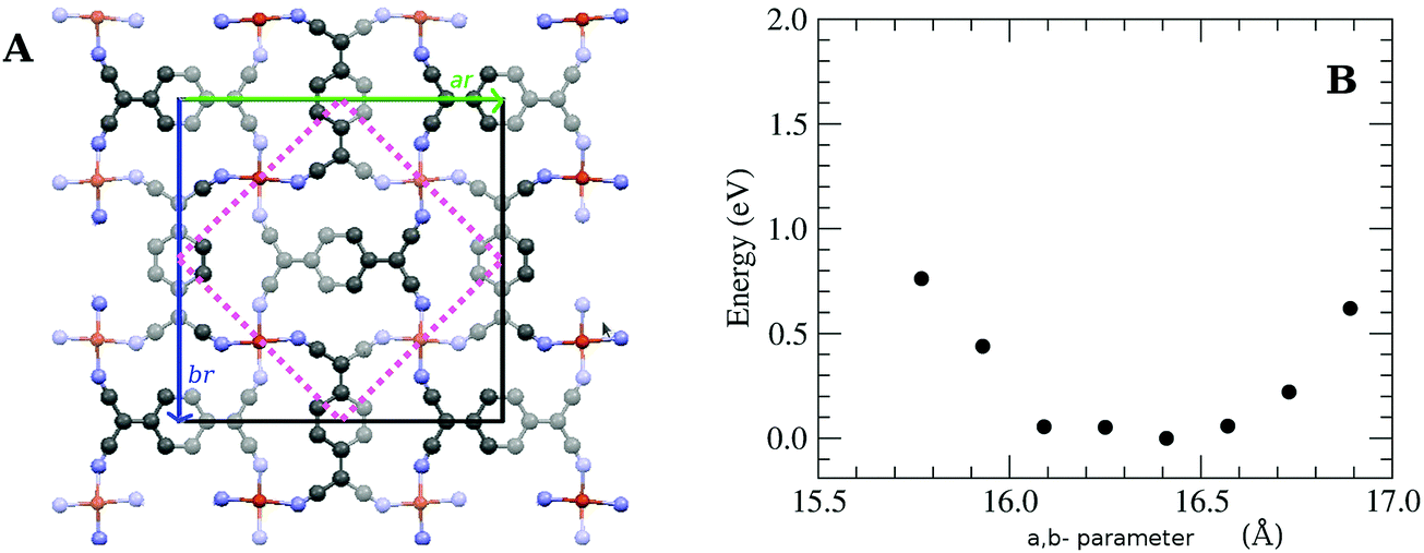 | ||
| Fig. 2 (A) Structure of the CuTCNQ ab-plane showing the irreducible parameter given by Heintz et al.13 and the ones used here. (B) Variation of the calculated total energy versus the in-plane lattice parameter in the CuTCNQ case, getting the approach a = b. | ||
Perpendicular to the surface direction, the MTCNQ film structure is driven by the TCNQ stacking forces. In order to determine these forces, a deep study of the structure was necessary along the c-axis direction. The optimized structures along this direction are shown in Fig. 3. A double cross-check between the experimental X-ray diffraction structure and the theoretical optimized structure was for the solids shown herein. In the TCNQ case, here used as a reference, the optimized TCNQ-molecular bond distances are comparable to those calculated by Long et al.29 within a maximum divergence of 1.2% with respect to the literature.32 The molecular packing is driven by N⋯N and CN⋯NC van der Waals-dispersion interactions, leading to an interleaving herringbone packing motif similar to that observed for benzene and aromatic fused-ring systems with the cell lattice previously given. The calculated molecular TCNQ inter-plane distance along the b-axis direction was 3.536 Å, while in the perpendicular to the TCNQ ring direction, it is 3.23 Å (because of the herringbone angle of 48.2°), which are comparable to those given by Long et al.29 This value is in agreement with a statistical study of the perpendicular stacking distance of all TCNQ and MTCNQ compounds that gave an average distance of 3.3 Å,33 indicating that the stacking in both organic-TCNQ and organometallics-MTCNQ structures is led by the same driving forces.
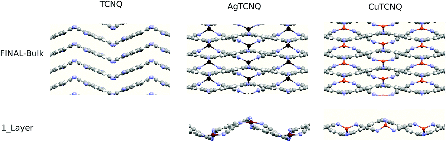 | ||
| Fig. 3 Final calculated structures for TCNQ and its organometallic MTCNQ. | ||
In the stacking c-direction, both MTCNQ films are characterized by a double herringbone structure of TCNQ molecules with the metal with a very distorted tetrahedral coordination. In the AgTCNQ case, the c-axis (where c = 6.975 Å), the TCNQ forms two independent stacks parallel to it with two different stacking distances of 3.34 Å and 3.66 Å. The mean interplanar distance within the TCNQ stacks was 3.50 Å (half of the c-axis value), which is close to the van der Waals value observed for this molecule in its own crystal. In the CuTCNQ case, Heintz et al.13 describes its structure as a unique stacking TCNQ distance, where the quinoid rings of the TCNQ units are engaged in interplanar stacking at a minimum distance of 3.24 Å. However, there is a divergence in the c-axis values in the literature,8,13,34,35 mainly due to the almost absence of Bragg peaks related to the c-axis in the powder. Xiao et al.35 found, by electron diffraction in a nanowire, a Bragg peak assigned to the (001)-CuTCNQ c-axis at 2θ = 25.52°, which corresponds c = 3.54 Å at their working wavelength. Our experimental X-ray diffraction data of the specular rod (00l) showed the presence of a low intense and broad peak close to the l = 1 in a perpendicular momentum transfer (see Fig. 4A). Due to the diffraction geometry used, the specular rod (00l) only had information about the atoms coordinates perpendicular to the surface (h = k = 0). The reciprocal space, i.e., the Miller indexes, was defined with respect to the Cu substrate lattice parameters. Therefore, the l = 1 corresponds to a d-spacing of 3.65 Å (lattice constant for Cu). The bulk Cu crystal has peaks at l = 2 and 4 but not at l = 1 due to a systematic absence (forbidden brag peak). This fact means that the aforementioned broad peak observed at l = 1.028 can only arise from the diffraction of the CuTCNQ overlayer. Taking into account the reciprocal space scale imposed by the Cu substrate, this gives a CuTCNQ c lattice constant of 3.51 ± 0.10 Å. Although the peak broadening gives a low precision in the perpendicular to the substrate film lattice value, the theoretical calculation gives a very flat minimum energy for a c lattice parameter of 3.62 Å, which is in very good agreement with our experimental value (see Fig. 4B). The resulting structure has the quinoid rings of the TCNQ units within the interplanar stacking at a minimum distance of 3.24 Å, which agrees with the distances given by Heintz et al.13 and Fernandez et al.9 The agreement of all the parameters for all the calculated structure with our X-ray diffraction data and the diffraction results found in the literature confirm the validity of the base and method used. Therefore, we can confirm that the presented bulk structures had the lowest energy structure, as compatible with the X-ray diffraction results. The only similar structure that could fit with our diffraction results is Rb-TCNQ.36 However the Rb-TCNQ is a structure closely related with our calculated structure and therefore this arrangement should have been explored during the energy minimization process of the calculation.
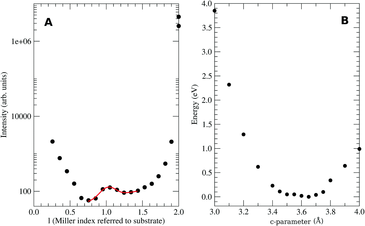 | ||
| Fig. 4 (A) Specular X-ray diffraction 00l crystal ROD intensity. The l Miller index is referred to perpendicular to the substrate surface lattice Cu(001) (with c = 3.615 Å); (B) calculated total energy of the CuTCNQ versus its c parameter. | ||
An interesting aspect derived from the calculations is the presence of other atomic arrangements of the metal atoms within the structure corresponding to a local minimum energy arrangement. In Fig. 5, we show some of these arrangements. These arrangements illustrate the high facility of the Cu atoms to move along the c-axis direction. The difference, in energy, between these minimums is small. This behavior explains the formation of the MTCNQ film starting from a well-ordered TCNQ film by means of the metal substrate atoms diffusion.16,37 During the diffusion, the Cu atoms pass through positions where their coordination changes from tetrahedral (4) to octahedral (6). Therefore, the TCNQ planes act as a sort of framework with pores, where the metal atoms are able to move along them extreme easily when subjected to external stimuli, such as an electrical field or optical effect irradiation. This fact means that this metal–organic framework (MOFs) represents a very interesting and open system for use in technological devices.9
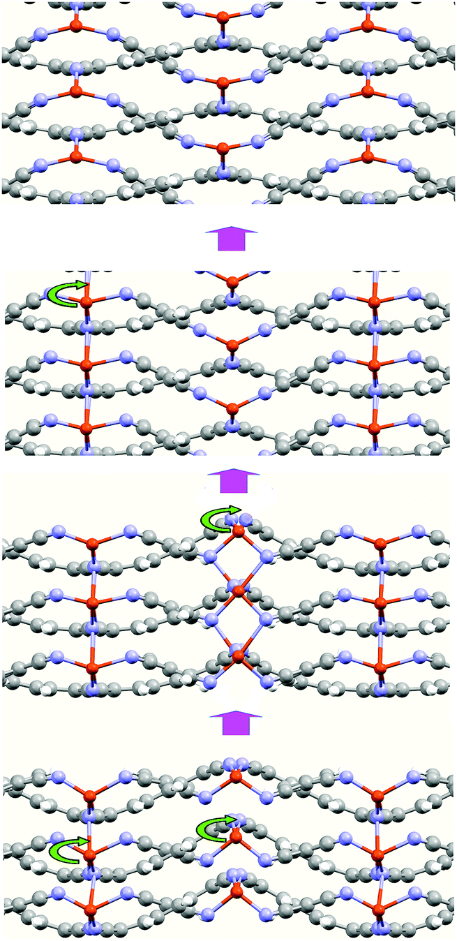 | ||
| Fig. 5 Snapshots of the CuTCNQ structure along the TCNQ stacking plane direction (c-axis) during optimization. These snapshots illustrate the mobility of the Cu atoms through the TCNQ-organic layers. | ||
II. The MTCNQ electronic structure
The total density of states (DOS) calculated for the bulk solids (solid line and dashed line) was compared to the results from the measured ultraviolet photoemission spectroscopy (UPS), shown as dots in Fig. 6. In this figure, it can be observed that the calculation reproduces all the tips characteristic of the experimental UPS very well. The calculated spectra are the result of the convolution of the theoretical DOS by a 0.25 eV width Gaussian curve.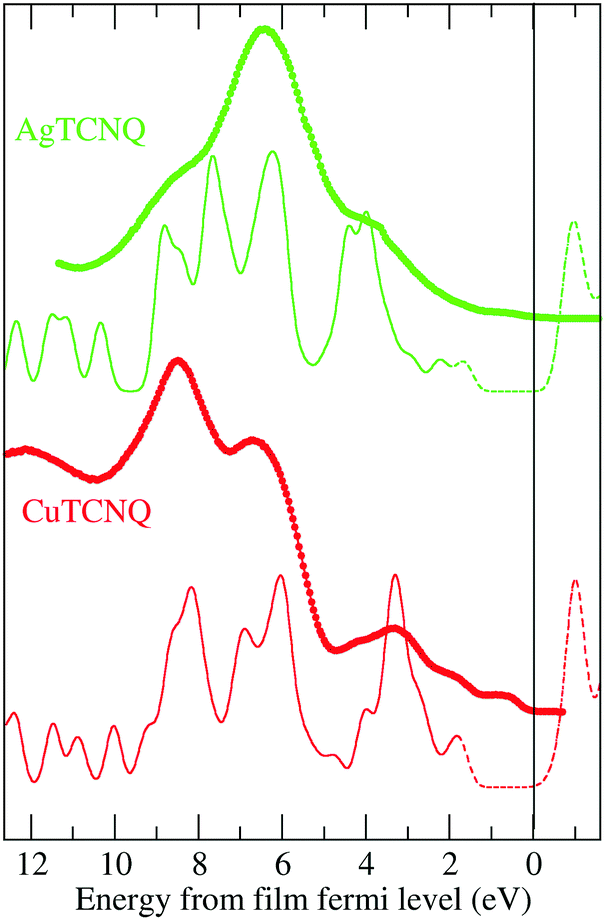 | ||
| Fig. 6 The calculated DOS compared to the measured UPS. The dots are the experimental data from UPS: green for AgTCNQ and red for CuTCNQ. The solid line is the calculated filled density of states, while the dashed line is the calculated empty density of states. The calculated DOS has been convoluted with a Gaussian of 0.25 eV full width half maximum. | ||
In order to determine the nature of the UPS characteristic tips, Fig. 7 shows the DOS calculated for the MTCNQ solids compared to the corresponding He-I and He-II UPS spectra. The used x-coordinate is different in the theoretical DOS and experimental spectroscopy, referred to as the MTCNQ Fermi level and to the substrate Fermi level, respectively. In both solids, there are empty states close to the Fermi level.
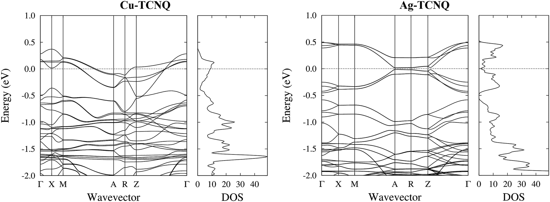 | ||
| Fig. 7 Detailed band structure and DOS for the bulk CuTCNQ (left panel) and the bulk AgTCNQ (right panel). The bands crossing the Fermi level are visible in the CuTCNQ case. For the AgTCNQ case, there are empty bands close to the Fermi level separated from the filled bands by a micro-gap in which is located the Fermi level. The density of states has been convoluted with a Gaussian of a width of 0.025 eV (one order of magnitude narrower than that used in the DOS presented in Fig. 6). | ||
The nature of these empty states close to the Fermi level can be elucidated in Fig. 7. This figure shows the calculated total density of states (DOS) convoluted with a Gaussian of 0.025 eV FWHM and the calculated band structure for the bulk MTCNQ (CuTCNQ in the left panel and AgTCNQ in the right panel). From the inspection of the DOS, it is clear the presence of the aforementioned empty states close to the Fermi level in both compounds. However, perusal of the band structure reveals that these states are of a different nature in each compound. For CuTCNQ, there are several bands crossing the Fermi level, while in the AgTCNQ case, there are no bands crossing the Fermi level. The bands close to the Fermi level are split by a quasi-symmetric way, with the filled bands and empty bands separated by a micro-gap and the Fermi level located inside the micro-gap. In summary: in CuTCNQ there are half-filled bands at the Fermi level; while in AgTCNQ, there are filled and unoccupied bands separated by a micro-gap. This difference in the nature of the empty states near the Fermi level is remarkable, given that these are two closely related compounds.
It is necessary to note that in Fig. 6, the experimental Fermi energy was determined by the Fermi edge of the metal substrate. At this scale, the Fermi energy of our calculations, determined as the boundary between the filled states (solid line) and the empty states (dashed line), did not match with the Fermi level of the substrate. Therefore, the x-scale for the calculated DOS must be shifted by around 2 eV with respect to the substrate Fermi level used in the experimental UPS spectra. With this correction, the observed features of the calculated DOS match very well with the observed UPS data. This can be explained by the following two facts. First, the CuTCNQ work function is 5.2 eV, which places the electron bands below the Cu substrate, which is 4.7 eV. As result of this, there is an electron injection from the substrate to the MTCNQ film, which results in the CuTCNQ Fermi level band becoming occupied, and as a consequence, this MTCNQ band is clearly visible in the UPS spectra. Second, there is a shift within the MTCNQ band gap, placing its Fermi energy at the edge of the conduction band. This is only possible by either band bending at the interface or by doping the MTCNQ structure with donors that provide electrons, thereby moving the Fermi level toward the conduction band edge (the dashed peak located at −1 eV above the Fermi level in Fig. 6). We can distinguish between these two cases. In the first case, the shift is limited to the interface and therefore depends on the MTCNQ layer thickness; while in the second case, the shift does not depend on the layer thickness. From our UPS results, in which we see a constant displacement independent of the MTCNQ thickness, and taking into account the limited sample depth of the UPS (one or two layers, depending on the photon energy), we can confirm that we have the second case. We consider that this is a doping of the CuTCNQ layer due to an excess of Cu diffusion from the substrate toward the supported films and, as reflected in the MTCNQ UPS spectra, this leads to an intense signal near the Fermi level. Indeed, the feature at 0.8 eV below the Fermi level that can be seen in the UPS spectra in Fig. 6 and 8 is the characteristic donor band corresponding to a highly doped n-type semiconductor.38 Thus, the excess of Cu atoms behave as donor impurities that lead to the Fermi level moving toward the lower edge of the conduction band. Thus, CuTCNQ behaves as an n-type semiconductor. This assumption is in agreement with the results from Sun et al.,39 who reported an n-type behavior for CuTCNQ films on Cu. The same happened in the AgTCNQ case.
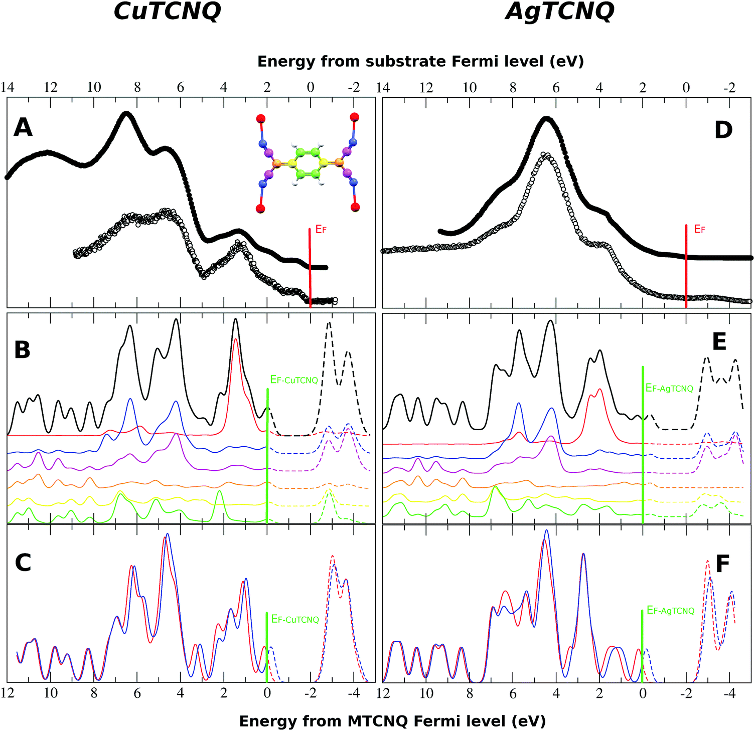 | ||
| Fig. 8 Partial density of states calculated for (B) CuTCNQ and (E) AgTCNQ compared to their corresponding experimental spectra (A) and (D). The filled circles correspond to He-I and the holed circles to the He-II measures. The color code used for the partial DOS corresponds to the color code shown in the MTCNQ molecule sketch in the inset in (A). (C) and (F) show the total DOS for a MTCNQ monolayer. The blue and red correspond to spin-up and down. Note that energy scale for panels A and D is referred to the experimental Fermi level, while the energy scale for panels B, C, E, and F is referred to the theoretical Fermi level. | ||
We have shown that the electronic structure of the CuTCNQ film goes from displaying a semiconductor behavior in Cu/CuTCNQ by band bending of the CuTCNQ bands induced by the substrate, to the above-described n-type semiconductor due to Cu–substrate doping. On the other hand, we have also shown that CuTCNQ acts as a metal–organic framework, where the metal can move very easily. We thus wondered if the possibility of these two electric states in the CuTCNQ films by changes in the mobility of doping atoms through the TCNQ induced by an external electric field could also contribute to the switching behavior exhibited by both CuTCNQ and AgTCNQ films.8 On the contrary, classic semiconductors, where the impurities are anchored in this metal–organic framework (MTCNQ), the impurities are spatially free. Therefore, an external field can induce a change in the film doping. In this direction, Deleruyelle et al.11 showed that resistive switching can occur due to the creation/dissolution of conductive filaments bridging the CuTCNQ surface to the AFM tip. They found in their system, where the CuTCNQ was not deposited on Cu-metal, a constant concentration of Cu+ was taken at the nanogap/CuTCNQ interface, meaning that CuTCNQ acted as an infinite Cu+ supplier. From our point of view, the observed switching electrical behavior could correspond to an alternate change between these two electronic states defined by the doping in MTCNQ. This can be an additional or alternate factor to the more accepted model that relates the switching behavior to the CuTCNQ interface. Basori et al.,40 using a simple metal–semiconductor–metal device model, found that the switching occurs primarily due to a lowering of the contact barrier at the cathode (the reversed bias junction) with an additional contribution arising from a lowering of the resistance of the CuTCNQ, although with less effect. The lowering of the contact potential agrees well with the qualitative mechanisms suggested before, where the formation of Cu filaments at the contacts has been suggested as the cause of switching. Lowering of the resistance of the CuTCNQ upon switching is a manifestation of non-linear conductance in the film, where upon switching a much larger current flows through the film. This mechanism could be used for changing the dopant concentration by simply changing the applied voltage (see Fig. 9). This effect, although coming from a different source, can be found in the mosfet transistors, where the conduction channel is opened by changing the minority concentration carriers by an electric field. Therefore, this could open up a large panorama of technological applications. In order to discard our model, we decided to measure the electric switch behavior with conductive AFM in a CuTCNQ/Cu system with growth under UHV conditions, as in our experiment, because in these conditions the oxide barrier should be absent, as the insulator interface is negligible in this case.
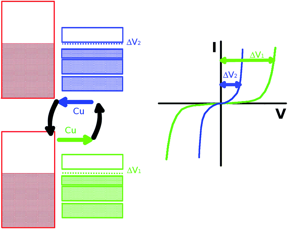 | ||
| Fig. 9 Sketch of the two electronic states of the CuTCNQ film depending on the film doping state. | ||
As a result of MTCNQ film doping, there was no electron band at the Fermi level. Considering the relationship between the appearance of shake-up peaks in the XPS with the presence of an empty band at the Fermi level,32 we attempted to show an absence of shake-ups in the C1s XPS in the MTCNQ case in opposition to the non-deposited TCNQ case. These absences were indeed experimentally observed in both MTCNQ solids.
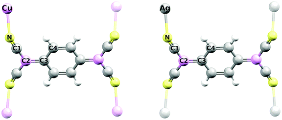
The partial DOS of the different atoms is shown by the different colored lines in Fig. 8B and E for CuTCNQ and AgTCNQ, respectively. The color code used for each atom is illustrated in the molecular sketch in the inset of Fig. 8A. In both MTCNQ solids, the first main peak comes from the metal electronic state and the next two bumps beside it come mainly from the cyano group atoms.
The XPS spectra of the MTCNQ show a single peak in the N1s edge and a double peak for the C1s (see Fig. 10) as is well known from the literature for TCNQ. However, there is a change in the relative intensity in the C1s peaks in the MTCNQ with respect to the TCNQ case. This change in intensity can be explained by the changes in the calculated charges shown in Table 1. In the TCNQ case, there are three different charges contributing to the most intense peak: the C-cyano (4 atoms per molecule), the C-bridge (8 atoms per molecule), and the C-ring in the other (4 atoms per molecule). The less positive atoms appear at a lower binding energy. In MTCNQ, two types of carbon bridges can be distinguished shifting toward the two extreme C-cyano and C-ring charges each. Thus, in Cu-TCNQ, the two peaks intensities become equivalent, which implies the 6 atoms per molecule contribution of each. Pink and green colors are used in the figure to show where each atom type contributes.
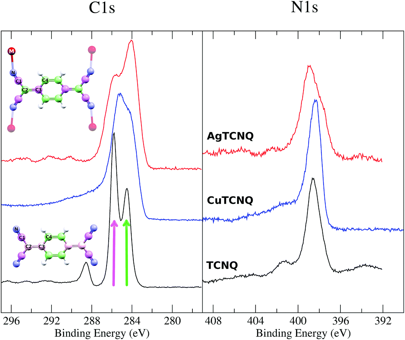 | ||
| Fig. 10 On the left C1s and on the right N1s XPS spectra for both CuTCNQ (blue line) and AgTCNQ (red line) films compared with the reference TCNQ film (black line). The color code (pink and green) is used to assign the atoms that contribute to the C1s XPS spectra. | ||
| TCNQ32 | CuTCNQ | AgTCNQ | |
|---|---|---|---|
| M | +0.527 | +0.456 | |
| N | −0.116 | −0.200 | −0.175 |
| C1-cyano | +0.027 | +0.068 | +0.062 |
| C2-bridge | +0.043 | −0.030 | −0.028 |
| C3-bridge | +0.046 | +0.026 | +0.027 |
| C4-ring | +0.001 | −0.019 | −0.017 |
No shake-up signal is observed in the C1s XPS, as was predicted, considering the previous electron band consideration based on our DOS calculations.
III. Monolayer MTCNQ magnetic behavior
The calculated density of states of one monolayer (1 ML) of the MTCNQ also showed very interesting magnetic properties for these solids. The optimized structure for the MTCNQ monolayer is shown in the lower panel of Fig. 3 and their corresponding DOS in Fig. 8C and F, for CuTCNQ and AgTCNQ, respectively. For this monolayer, the structure was calculated in both a spin-restricted regime and a spin-relaxed regime. In both cases, the structure was relaxed while searching the energy minimum. A clear difference between spin-up and the spin-down was observed, which implies magnetism in their monolayer. Table 2 shows the magnetism associated with each atom (in Bohr magnetons). In both solids, the magnetism is related to the N-cyano and the C2-bridge. In the case of CuTCNQ, the Cu also has a magnetic contribution. Although the charges shown in Table 2 are Voronoi, the magnetic moments shown in Table 2 are the difference between the up and down Mulliken charges. The difference in energy of the magnetic monolayers against their non-magnetic counterpart is ΔE = −71.611 meV for Ag-TCNQ and ΔE = −76.654 meV for the Cu case.|
|
||
|---|---|---|
| CuTCNQ | AgTCNQ | |
| M | +0.160 | +0.032 |
| N | +0.090 | +0.107 |
| C1-cyano | −0.027 | −0.031 |
| C2-bridge | +0.172 | +0.205 |
| C3-bridge | +0.055 | +0.070 |
| C4-ring | +0.033 | +0.038 |
| Unit cell | +4.131 | +3.932 |
In the CuTCNQ case, the magnetism in an increasing thickness slab was studied using the above-mentioned method. A large magnetism in 1 ML (+4.13 MB/4 molecules) was observed; whereas the magnetism was null in the 2 ML, small in 3 ML (+1.40 MB/4 molecules), and null in all the further increased thicknesses. This magnetic value was related to the presence of a double peak at the Fermi level in 1 ML (see Fig. 8C and F). Thus, incorporating an important magnetic behavior can be attempted when we grow an isolated species from metal 1 ML CuTCNQ or AgTCNQ, thus increasing the possibilities of the applications of these organometallic solids. The only experimental measurements of magnetism shown in literature are for the CuTCNQ and AgTCNQ bulks, which are almost null (AgTCNQ 0.0013 emu CGS per mol,41 CuTCNQ 0.0002 emu per mol = 0.178 MB13 compared with 10–1000 emu Oe per mol for MTCNQ, M = Co, Ni or Mn42). However, it is important to note that these results are theoretical results derived from our calculations for an isolated monolayer of CuTCNQ or AgTCNQ. In the presented experiments in which the MCTNQ layers were grown on top of a metal substrate, the charge injection from the metal substrate destroys the magnetic effect. A plausible experiment to confirm this magnetic behavior could thus be the growth of Cu or Ag in the under-monolayer regime on a non-metallic substrate (i.e., Al2O3) and the subsequent growth of a TCNQ layer by UHV deposition. After reaction of the TCNQ with the Cu, a magnetic layer of MTCNQ should be created, which could then be isolated from the substrate.
IV. Conclusions
We performed a systematic study of organometallic electron-acceptor molecules to answer all the issues arising from the study of the electronic properties of the film and its interface with a metal surface. From an experimental point of view, we used electron spectroscopies (XPS and UPS) for studying their electronic structure and X-ray diffraction for studying their physical structure. We performed double cross-checks of the experimental results with theoretical ab initio DFT calculations. These studies were performed on two closely related solids (CuTCNQ and AgTCNQ) as cross-checks that would allow us to identify the characteristic electronic features of each part of the molecules and their contribution to the final electronic structure. From these results, a complete description of the electronic structure of these molecular solid-films compatible with all the electronic spectroscopies measured was given.The study showed that the MTCNQ film acts as a metal–organic framework, where the Cu atoms have a large mobility. This result explains the large Cu–substrate diffusion in the former TCNQ film and which allows the growth of a structurally very controlled MTCNQ film on the metal substrate (with M = Cu or Ag, respectively). The diffusion extends along the whole TCNQ-film thickness. Furthermore, this large mobility allows an excess of metal coming from the substrate to act as donor impurities, making the MTCNQ behave as an n-type doped semiconductor. Contrary to the classic semiconductors, where the impurities are anchored to the semiconductor bulk, in this metal–organic framework, the impurities are spatially free. An external field can induce a drift of the metal atoms and, therefore, a change in the film doping. The conducting properties of the MTCNQ film can change depending on the doping concentration by the simple application of an external field. This effect, although coming from a different source, can be found in mosfet transistors, where the conduction channel is opened by changing the minority concentration carriers by an electric field. Therefore, this could be the basis for the possible contribution to the well-known switching behavior of CuTCNQ and AgTCNQ films when a non-insulator oxide is present in the metal–film interface. This opens up a large panorama of technological applications, such as flash memory devices.
We can resume the conclusions of this work in the following list:
(1) The MTCNQ film has a large diffusion power of metal atoms along the organic stacking direction. This explains both the capability of formation of the MTCNQ starting from TCNQ film by diffusion. It also explains the presence of an excess of metal in the MTCNQ film when it is grown on a metal substrate.
(2) The theoretical calculation of the DOS and band structure for MTCNQ shows the presence of empty states close to the Fermi level with a different nature depending of the compound, In Cu-TCNQ, there are half-filled bands at the Fermi level, while in Ag-TCNQ, the filled and unoccupied bands are separated by a micro-gap. This difference in the nature of the empty states near the Fermi level is remarkable given that these are two closely related compounds.
(3) As a consequence of this, the MTCNQ/M is an n-type semiconductor, where the excess diffused metal atoms act like donor impurities. This fully explains the position of the Fermi level and the shape of the measured UPS as well as the absence of shake-up features in the XPS spectra.
(4) The isolated MTCNQ monolayer also shows a very interesting magnetic behavior despite the non-magnetic behavior in the thicker films. It is interesting to note the different contributions to the magnetism of the metal in the CuTCNQ compared to in the AgTCNQ film.
(5) We proposed a new framework contribution to the switching electrical behavior of both CuTCNQ and AgTCNQ films over a metal substrate. In this metal–organic framework, where the impurities are spatially free, an external field can cause the metal atoms to drift, inducing a change in the film doping. The conducting properties of the MTCNQ film can change depending on the doping concentration by simply applying an external field.
Conflicts of interest
There are no conflicts to declare.Acknowledgements
This work was supported by the Spanish MICyT under grants No. MAT2013-47869-C4-3-P, FIS2016-74893-p and FIS2015-64886-C5-5-P. Parts of this research were carried out at the light source MAX-lab IV and Hasylab at DESY member of the Helmholtz Association (HGF). We would like to thank Dr O. Seeck his for assistance in using beamline W1.References
- E. Menard, M. A. Meitl, Y. Sun, J.-U. Park, D. J.-L. Shir, Y.-S. Nam, S. Jeon and J. A. Roggers, Chem. Rev., 2007, 107, 1117–1160 CrossRef PubMed
.
- W. Gao, J. Appl. Phys., 2003, 94, 359 CrossRef
- P. Peumans, V. Bulovic and S. R. Forrest, Appl. Phys. Lett., 2000, 76, 3885 CrossRef
- W. C. Chih, J. Y. Ouyang, J. H. Tseng and Y. Yang, Adv. Mater., 2005, 15, 1440 Search PubMed
-
K. Sienicki, Molecular Electronics and Molecular Electronic Devices, CRC Press, Boca Raton FL, 1994 Search PubMed
- R. S. Potembe, R. C. Hoffma, H. S. Hu, J. E. Cocchiaro, C. A. Viands and T. O’Poehler, Polym. J., 1987, 19, 147–156 CrossRef
- T. Oyamada, H. Tanaka, K. Matsushige, H. Sasabe and C. Adachi, Appl. Phys. Lett., 2003, 83, 1252 CrossRef
- Z. Gu, H. Wu, Y. Wei and J. Liu, J. Phys. Chem., 1993, 97, 2543–2545 CrossRef
- C. A. Fernandez, P. C. Martin, T. Schael, M. E. Bowden, P. K. Thallapally, L. Dang, W. Xu, X. Chen and B. P. McGrail, Sci. Rep., 4, 6114 CrossRef PubMed
- R. S. Potemberg, T. O. Poehler and D. O. Cowan, Appl. Phys. Lett., 1979, 34-6, 405 CrossRef
- D. Deleruyelle, C. Muller, J. Amoroux and R. Müller, Appl. Phys. Lett., 2010, 96, 263504 CrossRef
-
T. Kever, Resistive switching in Cu:TCNQ thin films, PhD thesis, Institut fürWerkstoffe der Elektrotechnik of the Rheinisch-Westfälische Technische Hochschule (RWTH) Aachen, Germany, 2009 Search PubMed
- R. A. Heintz, H. Zhao, X. Ouyang, G. Grandinetti, J. Cowen and K. R. Dunbar, Inorg. Chem., 1999, 38(1), 144–156 CrossRef
- A. K. Neufeld, A. P. O'Mullane and A. M. Bond, J. Am. Chem. Soc., 2005, 127, 13846–13853 CrossRef PubMed
- N. Gu, H.-Q. Zhang, Y. Wei, H.-Y. Shen and L. Zhang, Supramol. Sci., 1998, 5, 691 CrossRef
- M. J. Capitán, J. Álvarez, C. Navío and R. Miranda, J. Phys.: Condens. Matter, 2016, 28, 185002 CrossRef PubMed
- M. J. Capitan, C. Navio, J. I. Beltran, R. Otero and J. Alvarez, J. Phys. Chem. C, 2016, 120, 26889 CrossRef
- P. Hohenberg and W. Kohn, Phys. Rev. B: Condens. Matter Mater. Phys., 1964, 136, 864 CrossRef
- W. Kohn and L. J. Sham, Phys. Rev. A, 1965, 140, A1133 CrossRef
- P. Ordejon, E. Artacho and J. M. Soler, Phys. Rev. B: Condens. Matter Mater. Phys., 1996, 53, R10441 CrossRef
- J. M. Soler, E. Artacho, J. D. Gale, A. Garcia, J. Junquera, P. Ordejon and D. Sanchez-Portal, J. Phys.: Condens. Matter, 2002, 14, 2745 CrossRef
- J. Fraxedas, Y. J. Lee, I. Jiménez, R. Gago, R. M. Nieminen, P. Ordejón and E. Canadell, Phys. Rev. B: Condens. Matter Mater. Phys., 2003, 68, 195115 CrossRef
- G. R. Bhadua, J. C. Chaudharia, B. Rebarya, R. Patidara and D. N. Srivastavaa, Micron, 2018, 107, 85–93 CrossRef PubMed
- O. F. Sankey and D. J. Niklewski, Phys. Rev. B: Condens. Matter Mater. Phys., 1989, 40, 3979 CrossRef
- J. P. Perdew and Y. Wang, Phys. Rev. B: Condens. Matter Mater. Phys., 1992, 45, 13244 CrossRef
- G. Román-Pérez and J. M. Soler, Phys. Rev. Lett., 2009, 103, 096102 CrossRef PubMed
- R. Dion, H. Rydberg, E. Schroder, D. C. Langreth and B. I. Lundqvist, Phys. Rev. Lett., 2004, 92, 246401 CrossRef PubMed
- M. Methfessel and A. T. Paxton, Phys. Rev. B: Condens. Matter Mater. Phys., 1989, 40, 3616 CrossRef
- R. E. Long, R. A. Sparks and K. N. Trueblood, Acta Crystallogr., 1965, 18, 932 CrossRef
- T. Salzillo, M. Masino, G. Kociok-Kohn, D. Di Nuzzo, E. Venuti, R. G. D. Valle, D. Vanossi, C. Fontanesi, A. Girlando, A. Brillante and E. Da Como, Cryst. Growth Des., 2016, 16, 3028 CrossRef
- L. Shields, J. Chem. Soc., Faraday Trans. 2, 1985, 81, 1 RSC
- M. J. Capitan, J. Alvarez and C. Navio, Phys. Chem. Chem. Phys., 2018 Search PubMed
- J. Huang, S. Kingsbury and M. Kertesz, Phys. Chem. Chem. Phys., 2008, 10, 2625–2635 RSC
- Y. Wei and Z. Z. Gu, J. Southeast Univ., 1992, 22, 3 Search PubMed
- K. Xiao, J. Tao, Z. Pan, A. A. Puretzky, I. N. Ivanov, S. J. Pennycook and D. B. Geohegan, Angew. Chem., Int. Ed., 2007, 46, 2650–2654 CrossRef PubMed
- B. Bodegom, J. L. Boer and A. Vos, Acta Crystallogr., Sect. B: Struct. Crystallogr. Cryst. Chem., 1977, 33, 602–604 CrossRef
- P. Liu, Y. Jiang, H. Xie, F. Guo and J. Li, Jpn. J. Appl. Phys., 2005, 44, L494–L496 CrossRef
- T. Higuchi, T. Tsukamoto, N. Sata, M. Ishigame, Y. Tezula and S. Shin, Phys. Rev. B, 1998, 57, 6978 CrossRef
- Y. Sun, F. Zhang, Y. Sun, C.-a. Di, W. Xu and D. Zhu, J. Mater. Chem. A, 2015, 3, 2677–2683 RSC
- R. Basori, M. Kumar and A. K. Raychaudhuri, Sci. Rep., 2016, 6, 26764 CrossRef PubMed
- S. A. O'Kane, R. Clerac, H. Zhao, X. Ouyang, J. R. Galán-Mascarós, R. Heintz and K. R. Dunbar, J. Solid State Chem., 2000, 173, 152–159 Search PubMed
- E. B. Vickers, I. D. Giles and J. S. Miller, Chem. Mater., 2005, 17, 1667–1672 CrossRef
| This journal is © the Owner Societies 2018 |