
 Open Access Article
 This Open Access Article is licensed under a
 Creative Commons Attribution 3.0 Unported Licence
Exploring the electrochemical performance of graphite and graphene paste electrodes composed of varying lateral flake sizes†
Anthony J.
Slate
 ab,
Dale A. C.
Brownson
*ab,
Ahmed S.
Abo Dena
cd,
Graham C.
Smith
e,
Kathryn A.
Whitehead
a and
Craig E.
Banks
*ab
ab,
Dale A. C.
Brownson
*ab,
Ahmed S.
Abo Dena
cd,
Graham C.
Smith
e,
Kathryn A.
Whitehead
a and
Craig E.
Banks
*ab
aFaculty of Science and Engineering, Manchester Metropolitan University, Chester Street, Manchester, M1 5GD, UK. E-mail: d.brownson@mmu.ac.uk; Tel: +44 (0)1612476561
bManchester Fuel Cell Innovation Centre, Manchester Metropolitan University, Chester Street, Manchester M1 5GD, UK. E-mail: c.banks@mmu.ac.uk; Web: http://www.craigbanksresearch.com Tel: +44 (0)1612471196
cFaculty of Oral and Dental Medicine, Future University in Egypt (FUE), New Cairo, Egypt
dNational Organization for Drug Control and Research (NODCAR), P.O. Box 29, Giza, Egypt
eFaculty of Science and Engineering, Department of Natural Sciences, University of Chester, Thornton Science Park, Pool Lane, Ince, Chester CH2 4NU, UK
First published on 11th July 2018
Abstract
We report the fabrication, characterisation (SEM/EDX, TEM, XRD, XPS and Raman spectroscopy) and electrochemical properties of graphite and graphene paste electrodes with varying lateral flake sizes. The fabricated paste electrodes are electrochemically analysed using both outer-sphere and inner-sphere redox probes, namely; hexaammineruthenium(III) chloride, N,N,N′,N′-tetramethyl-p-phenylenediamine (TMPD), potassium ferrocyanide(II) and ammonium ferrous(II) sulphate. Upon comparison of different graphite paste electrodes, a clear correlation between the lateral flake sizes (La), ranging from 1.5 mm–0.5 μm, and electrochemical activity (heterogeneous electron transfer (HET) kinetics) is evident, where an improvement in the HET is observed at smaller lateral flake sizes. We infer that the beneficial response evident when employing laterally smaller flakes is due to an increased number of edge plane like-sites/defects available upon the electrode surface, facilitating electron transfer. Interestingly, given that the overall lateral flake sizes of the graphenes utilised (10.0–1.3 μm) were significantly smaller than those studied previously, an improvement in HET kinetics was also evident with the reduction of lateral flake size; the extent to which is redox-probe dependent. Improvements are observed up to a distinct point, termed the ‘lateral size threshold’ (ca. ≤2 μm) where the electrochemical reversible limit is approached. Further support is provided from density functional theory (DFT), exploring the electronic structure (i.e. HOMO–LUMO) as a function of flake size, which demonstrates that the coverage of edge plane like-sites/defects comprising the geometric structure of the relatively small graphene flakes is such that effectively the entire flake has become electrochemically active. In this study, the importance of lateral flake size with respect to electrochemical reactivity at carbon-based electrodes has been demonstrated alongside a structural relationship upon HET performance, a phenomenon that has not previously been described in the literature. Such work is both highly important and informative for the field of electrochemistry and electrode performance, with potential implications in a plethora of areas, ranging from novel renewable energy sources to electroanalytical sensing platforms.
Introduction
Carbon-based paste electrodes are widely utilised due to their advantageous attributes, such as exhibiting large potential domains, low background currents, their ease of modification and rapid surface regeneration.1,2 Recently, the use of graphitic paste electrodes has been at the forefront of research innovation given their universal requisition, combining the beneficial properties of novel carbon-based materials (i.e. graphene/graphite) with the significant benefits of paste electrodes. The study of graphene, ‘a single carbon layer of the graphite structure’,3,4 is of significant research interest due to its reported unique properties and beneficial application in numerous fields.5–7 Graphene is frequently employed in fundamental scientific studies to gain an enhanced understanding of how graphitic structures perform and behave given that its structure is the quantum of carbon electrodes (i.e. the minimalist structure) and investigations upon its electrochemical properties have aided the exploration, discovery and understanding of new carbon electrochemistry.3,5,8–11The surfaces of graphene and graphite are heterogeneous (anisotropic) in nature, with the overall chemical and electrochemical reactivity differing greatly between two distinct structural contributions, namely the edge and basal planes, which are fundamental to the behaviour of such electrodes.12,13 The current accepted understanding is that the predominate origin of heterogeneous electron transfer (HET) kinetics on such electrodes originates primarily from the reactivity of edge plane like-sites/defects and that inversely, the basal planes are effectively inert.5,12,14–16 Interestingly, the majority of fundamental studies explore the electrochemical properties of such distinct structural contributions via focusing particularly on the orientation of highly ordered pyrolytic graphite (HOPG) or more recently through the comparison of graphene's layer numbers, i.e. single- vs. quasi- vs. multi-layers.5,8,12,17
A key structural factor of graphitic flakes that may have been overlooked is their intraplanar microcrystallic size (La), i.e. the lateral flake size. There is a notable lack of investigations concerning the effects on the observed electrochemistry of changing the lateral flake size at graphene/graphite electrodes and thus, this is not fully understood to date. Evidently, changing the lateral flake size of a graphene/graphite sheet will in turn alter the relative structural contributions of edge/basal plane sites and thus the ‘edge-to-basal plane ratio’ of the material. Hence, the former will offer insights into the distinct electrochemical HET properties of edge and basal plane structures, as the flake size is altered along with the critical ratio/structural contributions. It is this important gap in knowledge that is addressed in this paper; the understanding of which will contribute towards the fundamental knowledge of these materials.
A major issue in graphene/graphite research, particularly in electrochemistry, is how to connect to (and electrically wire) graphene in order to explore its fundamental properties in a stringent and controlled/reproducible manner.2,18,19 The most common approach when utilising graphene is to immobilise it upon a suitable electrode surface and average the response over the graphene domains present. However, modifying such surfaces has the potential to leave underlying ‘reactive’ surfaces exposed, potentially interfering with the reported electrochemical reactivity.3 To overcome this issue, researchers have recently turned to fabricating three-dimensional graphene architectures,20–23 or utilising graphene paste electrodes comprised primarily of the material in question.2,24–28 In this latter case, with respect to observing the effects of altering graphene/graphite lateral flake size on the electrochemical properties, utilising the paste electrode set-up enables the reproducible electrical wiring of graphitic electrode materials in order to acquire electrochemical readings, whilst maintaining stringent/diligent controls and limiting other variable factors.
Given the above insights, in this paper, we report the fabrication, physicochemical characterisation and electrochemical performance of graphite and graphene paste electrodes with varying lateral flake sizes. Four graphite and five graphene powders with varying lateral flake sizes, ranging from ca. 1.5 mm to 0.5 μm were selected in order to establish if the difference in lateral flake size, La, and therefore the edge plane density of the electrode surface, has an effect upon the electrode's electrochemical behaviour/properties. We utilise density functional theory (DFT) calculations to confirm the experimental observations and reveal fundamental knowledge based upon these unique electrodes, demonstrating a structural relationship with respect to the geometrical contributions (i.e. edge and basal ratios) of graphitic materials and their electrochemical properties/performance.
Experimental section
All chemicals (of analytical grade or higher) were used as received from Sigma-Aldrich (UK) without any further purification. All solutions were prepared with deionised water of resistivity not less than 18.2 MΩ cm and were vigorously degassed prior to electrochemical measurements with high-purity, oxygen-free nitrogen. The redox probes utilised were as follows: hexaammineruthenium(III) chloride; potassium ferrocyanide(II); and N,N,N′,N′-tetramethyl-p-phenylenediamine (TMPD), which (unless otherwise stated) were prepared separately in solution at a concentration of 1 mM with 0.1 M KCl supporting electrolyte. Conversely, ammonium ferrous(II) sulphate was solubilised at 1 mM in 0.2 M perchloric acid.Voltammetric measurements were performed using an ‘Autolab PGSTAT 101’ (Metrohm Autolab, The Netherlands) potentiostat and data was controlled (generated and collected) using the software NOVA (Version 2.0). All measurements were conducted using a three-electrode system. The working electrode was either a graphene or graphite paste electrode (see below), with a platinum wire and saturated calomel electrode (SCE) employed as the counter/auxiliary and reference electrodes respectively. Note that where voltammetric scan rate studies are employed, the following increments were utilised within the specific ranges stated; 5, 10, 15, 25, 50, 75, 100, 150, 250 and 500 mV s−1.
For scanning electron microscope energy-dispersive X-ray microanalysis (SEM-EDX), transmission electron microscopy (TEM), X-ray diffraction (XRD), X-ray photoelectron spectroscopy (XPS) and Raman spectroscopy analysis, the respective powders were used as received from the supplier without any modifications. SEM images and surface element analysis were obtained using a JEOL JSM-5600LV model SEM, which was also equipped with an EDX microanalysis package. TEM images were obtained with a JEOL JEM-2010 (Oxford, Inca Energy TEM 100, UK). XRD was performed using an “X'pert powder PANalytical model” with a copper source of Kα radiation (of 1.54 Å) and Kβ radiation (of 1.39 Å), using a thin sheet of nickel with an absorption edge of 1.49 Å to absorb Kβ radiation. XPS data was acquired using a bespoke ultra-high vacuum system fitted with a Specs GmbH Focus 500 monochromated Al Kα X-ray source, Specs GmbH Phoibos 150 mm mean radius hemispherical analyser with 9-channeltron detection, and a Specs GmbH FG20 charge neutralising electron gun (XPS, K-Alpha, Thermo Scientific UK). All spectra were collected using Al–K radiation (1486.6 eV) monochromatized by a twin crystal monochromator, yielding a focused X-ray spot with a diameter of 400 μm, at 3 mA × 12 kV. The alpha hemispherical analyser was operated in the constant energy mode with survey scan pass energies of 200 eV to measure the whole energy band and 50 eV in a narrow scan to selectively measure the particular elements. Thus, XPS provided the chemical bonding states as well as the elemental composition of the graphene/graphite powders analysed. Charge compensation was achieved with the system flood gun that provides low energy electrons and low energy argon ions from a single source.30 Raman spectroscopy was obtained using a ‘Renishaw InVia’ spectrometer, which was equipped with a confocal microscope (×50 objective) spectrometer and an argon laser (514.3 nm excitation). Measurements were performed at a low laser power level (0.8 mW) to avoid any potential heating effects.31,32
Sourcing graphene and graphite powders with varying lateral flake sizes
Graphite and graphene powders were commercially obtained from Graphene Supermarket (Reading, USA).29 The graphite powders were Kish graphite, Flake graphite, High Crystalline Natural (HCN) graphite and Nanostructured graphite-250. The graphite flakes were independently measured via SEM and TEM in order to determine an average lateral flake size (N = 20) and comprised average lateral flake sizes of 1390.0 (±147.5) μm, 608.0 (±39.8) μm, 12.2 (±0.7) μm and 0.5 (±0.1) μm for Kish graphite, Flake graphite, High Crystalline Natural (HCN) graphite and Nanostructured graphite-250, respectively. The graphene powders comprised average lateral flake sizes of 9.4 (±0.7) μm, 5.0 (±0.3) μm, 4.0 (±0.3) μm, 2.3 (±0.5) μm and 1.3 (±0.1) μm for AO-1, AO-3, AO-4, AO-2, and C1, respectively. Note that a sample naming system has been utilised as commercially sourced and will enable interested readers to independently validate this work. The graphitic flakes used within this study have not been oxidised, reduced or chemically modified prior to electrochemical experiments (see below and the ESI† for full physicochemical characterisation). An edge-plane pyrolytic graphite (EPPG) electrode was utilised as a control to allow for appropriate comparisons to be made.19Fabrication of the graphene and graphite paste electrodes
The relevant graphitic paste mixtures were prepared by adding ca. 600 mg of a selected graphite/graphene powder with ca. 400 mg of mineral oil (Nujol) in a 60![[thin space (1/6-em)]](https://www.rsc.org/images/entities/char_2009.gif) :40 (% weight) composition, followed by vigorous hand-mixing until the paste was homogeneous. This composition was optimised by comparing the electrode constituents at a variety of ratios and monitoring the peak height, peak-to-peak separation (ΔEP) and reversibility against the standardised hexaammineruthenium(III) chloride and potassium ferrocyanide(II) redox probes. The mixtures were homogenised for 30 min prior to being compressed into a piston-driven polymeric-composite electrode shell. The polymeric cylindrical shell possessed an inner diameter of 4.5 mm, defining the working electrode's surface area. An electrical contact point was positioned at the rear of the paste electrode, with an electrical wire connecting the front ‘working surface’ of the paste electrode to the electrical contact point at the rear, allowing one to quantify the electrochemical behaviour demonstrated. Before experimental use, the paste electrode was prepared by applying pressure in order to force out a small portion of the paste. The paste electrode's ‘working surface’ was then polished against clean, lint-free filter paper, until a smooth/uniform working area was obtained. Finally, the surface was washed with deionised water prior to commencing electrochemical analysis. The calculated geometric area of the graphitic paste electrodes used throughout this study was 0.201 cm2 while the calculated geometric area of the control EPPG electrode was 0.196 cm2.
:40 (% weight) composition, followed by vigorous hand-mixing until the paste was homogeneous. This composition was optimised by comparing the electrode constituents at a variety of ratios and monitoring the peak height, peak-to-peak separation (ΔEP) and reversibility against the standardised hexaammineruthenium(III) chloride and potassium ferrocyanide(II) redox probes. The mixtures were homogenised for 30 min prior to being compressed into a piston-driven polymeric-composite electrode shell. The polymeric cylindrical shell possessed an inner diameter of 4.5 mm, defining the working electrode's surface area. An electrical contact point was positioned at the rear of the paste electrode, with an electrical wire connecting the front ‘working surface’ of the paste electrode to the electrical contact point at the rear, allowing one to quantify the electrochemical behaviour demonstrated. Before experimental use, the paste electrode was prepared by applying pressure in order to force out a small portion of the paste. The paste electrode's ‘working surface’ was then polished against clean, lint-free filter paper, until a smooth/uniform working area was obtained. Finally, the surface was washed with deionised water prior to commencing electrochemical analysis. The calculated geometric area of the graphitic paste electrodes used throughout this study was 0.201 cm2 while the calculated geometric area of the control EPPG electrode was 0.196 cm2.
In order to electrochemically characterise the fabricated graphite paste electrodes and to evaluate the effect that varying the lateral flake size induces upon the HET properties, well-known and widely understood outer- and inner-sphere electrochemical redox probes were used (see ESI† for more information), namely hexaammineruthenium(III) chloride, TMPD, potassium ferrocyanide(II) and ammonium ferrous(II) sulphate. Furthermore, it has been reported that, when present, surfactants (such as Nafion and Sodium Cholate) can interfere with and even dominate the observed electrochemical response.71–73 Herein, we have performed ‘blank’ controls to ensure that the Nujol utilised does not give rise to electrochemical peaks that interfere with experimental observations. Typical cyclic voltammetric responses obtained at each of the fabricated paste electrodes (graphene and graphite) in 0.1 M KCl electrolyte are depicted in Fig. S16 and S17 (ESI†), where within both the anodic and cathodic potential regions of interest herein, there are no evident voltammetric peaks prior to the addition of the redox probes studied. Moreover, the composition of each fabricated electrode (in terms of the Nujol) was kept constant, mitigating this as a variable and therefore the observed changes in the electrochemistry are deemed representative only of the alterations imposed on the carbon structure, namely the graphene/graphite lateral flake sizes.
Determination of the heterogeneous electron transfer rate/kinetics (k0)
The Heterogeneous Electron Transfer (HET) rate constant (k0) values for the various graphitic-based paste electrodes were calculated using the Nicholson equation for an electrochemically quasi-reversible process, as described by eqn (1):33| ψ = k0[(πDnvF)/(RT)]−1/2 | (1) |
| ψ = (−0.6288 + 0.0021X)/(1 − 0.017X) | (2) |
 | (3) |
Determination of the electrochemical effective/active area of the graphite/graphene electrodes
The electrochemical effective area (Aeff) of the graphite and graphene paste electrodes was calculated with the Randles–Ševčík equation at room temperature (298 K), for an electrochemically quasi-reversible process using the following equation:41| IP = (2.65 × 10⁵)n3/2D1/2v1/2CAeff | (4) |
 | (5) |
Determination of the ‘edge-to-basal plane ratio’
The ‘edge-to-basal plane ratio’ of the graphene/graphite paste electrodes was calculated using the total specific capacitance (C0). C0 was determined via cyclic voltammetry using 1 mM hexaammineruthenium(III) chloride in 0.1 M KCl at scan rates of 100, 200 and 500 mV s−1. The voltammetric window selected was in a non-Faradaic region (between 0.2 and 0.3 V, with capacitance values taken at 0.255 V (vs. SCE)).42,43 The potential range used has no Faradaic processes occurring, therefore cathodic and anodic current densities are associated with charging of the electrical double layer. The ‘difference between the anodic and cathodic current density’ at 0.255 V versus the corresponding ‘scan rate’ is plotted, such that the linear regression indicates the value of double layer capacitance. Alternatively, the C0 for each scan rate can be calculated using the following equation:42,43 | (6) |
| C0 = C0edgefedge + C0basal(1 − fedge) | (7) |
Density functional theory (DFT) computation
Gaussian 09W package software was used for all Density Functional Theory (DFT) calculations, including molecular geometry optimisation and molecular orbital (MO) calculations. The Beck's three-parameter hybrid (B3LYP) method was used for geometry optimisation and MO calculations.45 The B3LYP method gives results more accurate than semi-empirical and the pure Hartree–Fock level of theory.46 It represents a combination of Beck's three parameters with the correlation functional of Lee, Yang and Parr.47 The basis set 6-31G** was selected for all calculations because it is suitable for calculations carried out on large molecules (>100 atoms).48–52 The calculation results were visualised with the aid of GaussView 05 package software.53 The distribution of electrons in the highest occupied molecular orbital (HOMO) and lowest unoccupied molecular orbital (LUMO) were also visualised to predict the possible electron transfer processes and electrostatic potential maps were visualised to investigate the distribution of electronic charges.Results and discussion
Physicochemical characterisation of the graphite and graphene electrode materials
Independent physicochemical characterisation of the various powders and fabricated paste electrodes was performed using SEM-EDX, TEM, XRD, XPS and Raman spectroscopy in order to ascertain the differences in structural and chemical properties. Fig. 1 depicts the SEM images (TEMs are presented in Fig. S1, ESI†) of the four graphite powders utilised. It is evident that the range of graphite powders comprise large interplanar microcrystalline sizes, Lc, which demonstrate the presence of multi-layer graphite, as expected. Importantly, the intraplanar microcrystalline size, La (lateral flake/grain size) of each powder varies significantly, which correlates with the expected ranges associated with the samples: ca. 1390.0 (±147.5) μm kish graphite; ca. 608.0 (±39.8) μm flake graphite; ca. 12.2 (±0.7) μm HCN graphite; and ca. 0.5 (±0.1) μm nanostructured graphite (see Table 1). Similarly, the TEM images (SEMs are presented in Fig. S2, ESI†) of the five graphene powders demonstrate that the graphenes exhibit an Lc size of ca. 0.34 nm and larger, indicating the combined presence of single layer graphene and quasi-graphene (Fig. 2).8,17,18,54 Again, the La (lateral flake/grain size) of each graphene powder varies, with the following average lateral flake size associated with the respective samples: ca. 9.4 (±0.7) μm AO-1; 5.0 (±0.3) μm AO-3; ca. 4.0 (±0.3) μm AO-4; ca. 2.3 (±0.5) μm AO-2 and ca. 1.3 (±0.1) μm C1 (Table 2). | ||
| Fig. 1 SEM images of the graphite powders used to fabricate the paste electrodes, showing individual lateral flake sizes; (A) kish graphite, (B) flake graphite, (C) HCN graphite, and (D) nanostructured graphite-250. Note, the variation in magnification, emphasising the difference in lateral flake size of the graphite flakes. | ||
| Graphite type used to fabricate paste electrode | Average measured lateral flake size (N = 20) (μm) | k 0 (cm s−1) | A eff (cm2) | A real (%) | ΔEP (mV) at 100 mV s−1 |
|---|---|---|---|---|---|
| Hexaammineruthenium(III) chloride/0.1 M KCl | |||||
| Kish graphite | 1389.9 (±147.5) | 1.69 × 10⁻³ | 0.169 | 84.1 | 141.0 (±2.8) |
| Flake graphite | 608.0 (±39.8) | 2.05 × 10⁻³ | 0.208 | 103.5 | 118.3 (±3.6) |
| HCN graphite | 12.2 (±0.7) | 3.35 × 10⁻³ | 0.147 | 73.1 | 85.6 (±7.1) |
| Nanostructure graphite-250 | 0.5 (±0.1) | 3.48 × 10⁻³ | 0.150 | 74.6 | 78.1 (±3.6) |
| TMPD/0.1 M KCl | |||||
| Kish graphite | 1389.9 (±147.5) | 1.42 × 10⁻³ | — | — | 130.9 (±41.1) |
| Flake graphite | 608.0 (±39.8) | 1.82 × 10⁻³ | — | — | 128.4 (±32.7) |
| HCN graphite | 12.2 (±0.7) | 1.95 × 10⁻³ | — | — | 115.9 (±24.7) |
| Nanostructure graphite-250 | 0.5 (±0.1) | 2.43 × 10⁻³ | — | — | 98.2 (±10.7) |
| Potassium ferrocyanide(II)/0.1 M KCl | |||||
| Kish graphite | 1389.9 (±147.5) | 6.04 × 10⁻⁵ | — | — | 833.4 (±1.1) |
| Flake graphite | 608.0 (±39.8) | 1.93 × 10⁻³ | — | — | 143.5 (±35.0) |
| HCN graphite | 12.2 (±0.7) | 1.79 × 10⁻³ | — | — | 105.8 (±7.1) |
| Nanostructure graphite-250 | 0.5 (±0.1) | 1.71 × 10⁻³ | — | — | 151.1 (±7.1) |
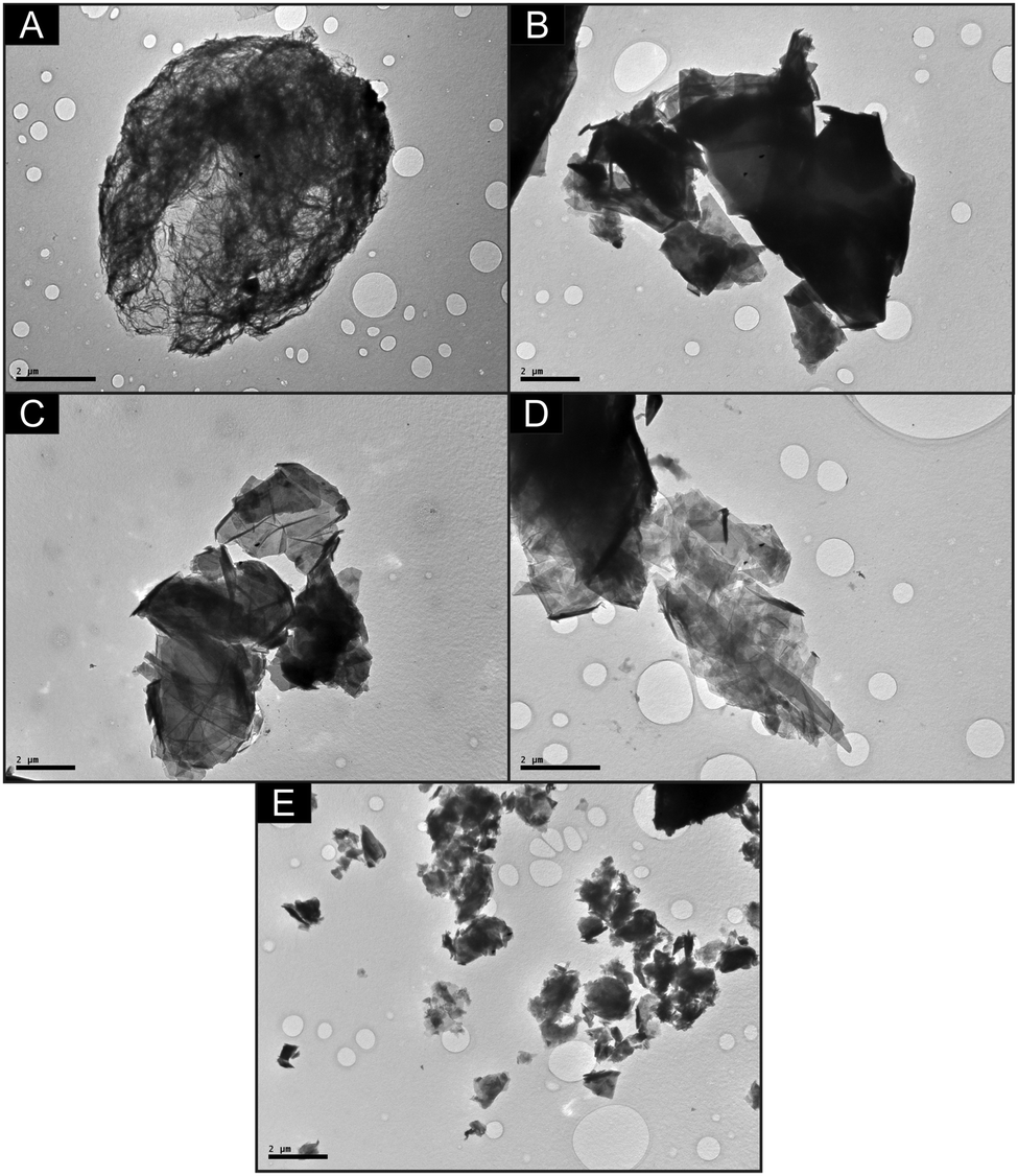 | ||
| Fig. 2 Structural characterisation of the graphene lateral flakes via TEM; (A) AO-1, (B) AO-2, (C) AO-3, (D) AO-4 and (E) C1. Note that the scale bar is 2 μm in all images. | ||
| Graphene type used to fabricate paste electrode | Average measured lateral flake size (N = 20) (μm) | k 0 (cm s−1) | A eff (cm2) | A real (%) | ΔEP (mV) at 100 mV s−1 |
|---|---|---|---|---|---|
| AO-1 | 9.4 (±0.7) | 2.37 × 10⁻³ | 0.083 | 41.2 | 93.2 (±3.6) |
| AO-3 | 5.0 (±0.3) | 2.75 × 10⁻³ | 0.190 | 94.5 | 85.6 (±14.3) |
| AO-4 | 4.0 (±0.3) | 2.99 × 10⁻³ | 0.162 | 80.6 | 73.0 (±2.0) |
| AO-2 | 2.3 (±0.5) | 4.38 × 10⁻³ | 0.225 | 111.9 | 65.5 (±3.6) |
| C1 | 1.3 (±0.1) | 5.45 × 10⁻³ | 0.115 | 57.2 | 64.5 (±3.6) |
For interested readers, Fig. S3 and S4 (ESI†) show SEM images of the surfaces of respective graphene and graphite paste electrodes following their fabrication.2 Moreover, Fig. S5–S9 (ESI†) depict additional TEM images of the graphene flakes (powders) that are utilised within this study.
Raman spectroscopy was performed on the four graphitic powders (with the spectra presented in Fig. S10, ESI†). The Raman spectra reveals two characteristic peaks at ca. 1579 and 2670 cm−1, which are due to the G and 2D (G′) bands, respectively.55–58 The intensity ratio of the G and 2D bands, the asymmetrical nature of the 2D (G′) band, in addition to the shoulder evident, are consistent with that expected for multi-layered graphite. The low/faint presence of a D band (ca. 1335 cm−1) indicates that the graphite samples are of high quality and possess a low level of basal plane crystal defects across their lattices.55–58 Interestingly, the intensity of the D bands increase as the graphitic lateral flake size decreases, which is likely related to the increment in the edge plane like-sites present, as this geometric contribution (edge plane) raises and diminishes the contribution of the basal plane within the edge/basal ratio. Fig. S11 (ESI†) depicts the Raman spectra of the five graphene powders, revealing two characteristic peaks (G and 2D (G′)) of graphitic materials at ca. 1579 and 2670 cm−1.55–58 The highly symmetrical 2D (G′) band peak and the intensity ratio of the G and 2D bands indicate that the surfaces comprise single- to few-layer graphene sheets. The presence of a small D band indicates that there are a small number of structural defects on the graphene surface (limited basal plane crystal defects, i.e. a lack of edge plane sites/defects), however as stated earlier, the relatively low intensity of the D bands suggests that generally an ordered graphene structure of high quality is present.55–58 Note that, in the case of AO-1, distinct Raman spectra are evident, in which the D band is significantly larger than that of the other graphene powders. In this instance, it is likely that the powder utilised contains a high number of edge plane like-sites/defects (giving rise to the large D band) which will likely influence the voltammetry observed and this must be considered.
The chemical composition of the various graphitic powders was characterised using a range of techniques (XRD, EDX and XPS) and this is reported in full in the ESI.†
The combined surface and physicochemical analysis confirms the presence of a range of high quality/purity graphitic nanosheets. It is clear that the low O/C ratio of the graphene and graphite powders are near that of a pristine nature, which in conjunction with the parallel features present in each of the samples, allows the consideration of only the structural (lateral flake size) changes within each of the powders and their effect on the electrochemical performance.
Graphite paste electrodes: electrochemistry at varied lateral flake sizes
The electrochemical system was first benchmarked and characterised using an EPPG electrode towards hexaammineruthenium(III) chloride (Fig. 3), which exhibits a peak-to-peak separation (ΔEP) of ca. 80.6 mV (at 100 mV s−1vs. SCE). This value is in agreement with previous literature, which is due to the electrode surface having a large global coverage of edge plane like-sites/defects, giving rise to fast heterogeneous electron transfer.8,16 In order to explore the effect of lateral flake size, cyclic voltammograms were obtained for each of the four respective graphite pastes (Fig. 3). A pair of well-defined redox peaks are evident when using each electrode, with ΔEP values observed at ca. 78.1, 85.6, 118.3 and 141.0 mV (100 mV s−1vs. SCE) for the nanostructured, HCN, flake and kish graphite materials, respectively. The ΔEP values indicate that, as the lateral flake size of the graphite paste electrodes decrease, the peak-to-peak separation decreases, suggesting that the electrochemical process becomes more reversible as the flake size is reduced. Indeed, this inference is supported via the k0 values obtained (see Table 1), which indicate that smaller lateral flake sizes result in improved HET.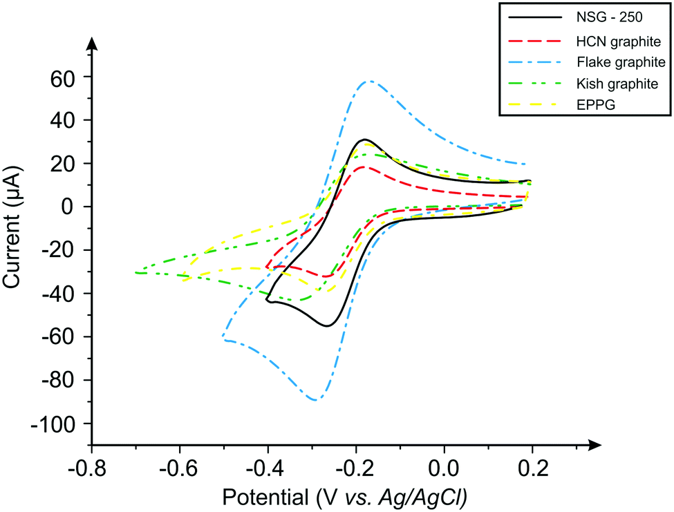 | ||
| Fig. 3 Typical cyclic voltammetric profiles recorded using graphite paste electrodes. Redox probe: 1 mM hexaammineruthenium(III) chloride/0.1 M KCl. Scan rate: 100 mV s−1. | ||
Further analysis of the cyclic voltammetric data reveals that nanostructured graphite, with the smallest lateral flake size, exhibits the fastest electron transfer rate (3.48 × 10⁻³ cm s−1), whilst kish graphite (the largest average lateral flake size) exhibited the slowest (1.69 × 10⁻³ cm s−1). One explanation for these observations is that the ‘edge-to-basal plane ratio’ is being altered as one varies the lateral flake size. Resultantly, as the lateral flake size of the graphite flakes decrease, the amount of edge planes available on the surface of the electrode increases (or the proportion of this compared to the other geometrical contribution, i.e. the un-reactive basal plane, which reduces in size). The calculated percentage ‘edge-to-basal plane ratio’ of the respective graphite electrodes correlates well with this inference, with improved electrochemical activity exhibited by electrodes with smaller lateral flake sizes (see Table 3). Resultantly, it was estimated (electrochemically) that kish graphite (average lateral flake size ca. 1390.0 (±147.5) μm) possessed an edge/basal plane percentage ratio of 1.16% edge/98.84% basal and that nanostructured graphite (average lateral flake size ca 0.5 (±0.1) μm) comprised of 27.99% edge/72.01% basal, respectively. These results indicate that smaller lateral flake sizes give rise to a higher % global coverage of edge plane like-sites/defects, which in turn results in improved HET properties and an electrochemically favourable response in contrast to larger lateral flake sizes.
| Carbon-based electrode material utilised | Average measured lateral flake size (N = 20) (μm) | Total specific capacitance (μF cm−2) | Edge plane (%) | Basal plane (%) | k 0 (cm s−1) |
|---|---|---|---|---|---|
| Graphite paste electrodes | |||||
| Kish graphite | 1389.9 (±147.5) | 0.20 | 1.06 | 98.94 | 1.69 × 10⁻³ |
| Flake graphite | 608.0 (±39.8) | 0.99 | 0.02 | 99.98 | 2.05 × 10⁻³ |
| High crystalline natural graphite | 12.2 (±0.7) | 0.23 | 1.11 | 98.89 | 3.35 × 10⁻³ |
| Nanostructured graphite-250 | 0.5 (±0.1) | 20.31 | 27.99 | 72.01 | 3.48 × 10⁻³ |
| Graphene paste electrodes | |||||
| AO-1 | 9.4 (±0.7) | 1.48 | 0.70 | 99.30 | 2.37 × 10⁻³ |
| AO-3 | 5.0 (±0.3) | 3.33 | 3.38 | 96.62 | 2.75 × 10⁻³ |
| AO-4 | 4.0 (±0.3) | 15.86 | 21.53 | 78.47 | 2.99 × 10⁻³ |
| AO-2 | 2.3 (±0.5) | 11.64 | 15.42 | 84.58 | 4.38 × 10⁻³ |
| C1 | 1.3 (±0.1) | 33.57 | 47.20 | 52.80 | 5.45 × 10⁻³ |
To ensure that the redox probes are not adsorbing onto the surface of the paste electrodes, logIPversus log scan rate (v) plots were explored utilising the hexaammineruthenium(III) probe. Results indicated semi-indefinite linear diffusion in all cases, as governed by the Randles–Ševčík equation (Table S3, ESI†). Confirming that the observations throughout this study are due to diffusional processes, with no contributions from surface adsorption.5,17 The calculated electrochemical effective area (Aeff) of the graphite paste electrodes ranged from 0.15 cm2 at HCN graphite to 0.21 cm2 for flake graphite.75
We next turn to TMPD, which is a ‘near’ outer-sphere redox probe,75 to further explore the above observations. In order to benchmark and characterise the TMPD redox probe, electrochemical analysis was first performed utilising an EPPG electrode (Fig. S18, ESI†), which exhibited a ΔEP of ca. 88.1 mV (100 mV s−1vs. SCE). The graphite paste electrodes were then electrochemically explored (Fig. S18, ESI†), with resulting k0 values demonstrating that the nanostructured graphite exhibits the fastest rate of electron transfer (2.43 × 10⁻³ cm s−1) followed by HCN graphite, flake graphite, and with the slowest k0 observed at kish graphite (1.42 × 10⁻³ cm s−1), see Table 1. Clearly, when utilising the (outer-sphere) TMPD redox probe, the nanostructured graphite electrode (with the smallest lateral flake size) exhibits the most favourable electron transfer properties/reactivity when compared to its graphitic counterparts, with the HET rate lowering as lateral flake sizes increase.
Next, potassium ferrocyanide(II), an inner-sphere redox probe, was utilised. Benchmarking with an EPPG electrode (Fig. S19, ESI†) revealed a peak-to-peak separation (ΔEP) of ca. 133.4 mV (100 mV s−1vs. SCE). Under the same conditions, the ΔEP values observed using the graphitic paste electrodes were ca. 105.8, 143.5, 151.1 and 833.4 mV for the HCN, flake, nanostructured and kish graphite respectively. The ΔEP values indicate that, with this particular probe, the HCN graphite exhibits the most reversible electron transfer process, whilst the kish graphite (largest average lateral flake size) is the least reversible. The k0 values obtained reveal that flake graphite was the most effective electrode utilised towards this probe, producing the largest estimated electron transfer rate (1.93 × 10⁻³ cm s−1), however, this was not significantly faster than HCN (1.79 × 10⁻³ cm s−1) and nanostructured graphite (1.71 × 10⁻³ cm s−1) which were similar in HET speeds. Crucially, kish graphite, which possesses the largest lateral flake size, gave rise to the most unfavourable electrochemical performance, with a k0 estimated at 6.04 × 10⁻⁵ cm s−1 (see Table 1). These findings correlate with the number of available edge plane like-sites/defects and with the inferences from above. Interestingly however, the close proximity of the estimated k0 values and hence the more reversible and similar voltammetry observed at the smaller lateral flake sizes in this case suggests that the surface structure (in terms of oxygenated species) could also be influencing the observed electrochemical properties towards this inner-sphere probe, or that the electrochemical reversible limit is approached for these flake sizes.
Ammonium ferrous(II)sulphate was the final inner-sphere redox probe utilised in this study and was selected due to its ability to demonstrate sensitivity towards the presence of surface oxides and functional groups. This is important since their presence can lead to catalysis by surface carbonyl groups and derivatization of C![[double bond, length as m-dash]](https://www.rsc.org/images/entities/char_e001.gif) O groups which could potentially be available on the surface of the graphitic paste electrodes.35,59,60,74 Previously, this probe reportedly demonstrated an unexpectedly large ΔEP when utilised towards a screen-printed graphite macro-electrode, producing a peak-to-peak separation of 434 mV.39 The ammonium ferrous(II)sulphate redox probe was characterised using an EPPG electrode (Fig. S20, ESI†) and exhibited a ΔEP of ca. 256.8 mV (100 mV s−1vs. SCE). The ΔEP values observed at the four graphitic paste electrodes were ca. 108.3, 136.0, 229.9 and 1027.2 mV for the flake, nanostructured, HCN and kish graphite, respectively (see Table S4 and Fig. S20, ESI†). It is worth noting that this probe did not produce well defined voltammetry with the HCN graphite paste electrode, possibly due to the inner-sphere nature and precise interactions between this specific redox probe and the electrode in question (and surface oxygenated species, if present); resultantly, the voltammogram for HCN was removed from the figure. The k0 values for this probe could not be accurately determined due to the lack of a reported diffusion coefficient in the literature, however, basing analysis upon the ΔEP values it is again clear that smaller lateral flake sizes give rise to improved electrochemical interactions.
O groups which could potentially be available on the surface of the graphitic paste electrodes.35,59,60,74 Previously, this probe reportedly demonstrated an unexpectedly large ΔEP when utilised towards a screen-printed graphite macro-electrode, producing a peak-to-peak separation of 434 mV.39 The ammonium ferrous(II)sulphate redox probe was characterised using an EPPG electrode (Fig. S20, ESI†) and exhibited a ΔEP of ca. 256.8 mV (100 mV s−1vs. SCE). The ΔEP values observed at the four graphitic paste electrodes were ca. 108.3, 136.0, 229.9 and 1027.2 mV for the flake, nanostructured, HCN and kish graphite, respectively (see Table S4 and Fig. S20, ESI†). It is worth noting that this probe did not produce well defined voltammetry with the HCN graphite paste electrode, possibly due to the inner-sphere nature and precise interactions between this specific redox probe and the electrode in question (and surface oxygenated species, if present); resultantly, the voltammogram for HCN was removed from the figure. The k0 values for this probe could not be accurately determined due to the lack of a reported diffusion coefficient in the literature, however, basing analysis upon the ΔEP values it is again clear that smaller lateral flake sizes give rise to improved electrochemical interactions.
Overall, the above trend indicates that, as the lateral flake size of carbon-based paste electrodes (such as those comprised of graphite) decreases, the electrochemical reactivity of the electrode increases. A reduction in the peak-to-peak separation (ΔEP) is evident, representing an improvement in electrochemical reversibility and HET rates (k0). It is inferred that these observations are directly related to the % of edge plane contribution comprising the graphite flake's geometry, which is further evidenced when one considers that the graphite electrodes most effective towards the outer-sphere redox probes were those with smaller lateral flake sizes and a higher estimated % global coverage of edge plane. Inversely, kish graphite has been shown consistently as the least effective of the four graphite paste electrodes, which possesses the largest average lateral flake size and hence the biggest basal plane % comprising its structure. Results are also reiterated with the inner-sphere probes, however, care needs to be taken over their interpretation given that oxygenated species and ligands found on the electrode surface influence the observed electrochemistry (unlike the case for outer-sphere probes, which are dependent only on the electronic density of states).61
Confirmation of the above trends can be gained through analysis of the average specific capacitance, C0, of the paste electrodes, which can also be utilised to determine the edge/basal ratios (see Table 3). It is clear that kish graphite (largest average lateral flake size) exhibits an estimated edge plane percentage of 1.06%, which when compared to nanostructured graphite-250 (smallest lateral flake size, with an edge plane percentage of 27.99%) and correlated with the observed electrochemical properties/performances, one can infer that indeed, as the lateral flake size of the material comprising the graphite paste electrode decreases, the percentage coverage of edge sites increases and this gives rise to favourable electrochemistry.
Graphene paste electrodes: electrochemistry at varied lateral flake sizes
The graphene-based paste electrodes were first evaluated with the outer-sphere redox probe 1 mM hexaammineruthenium(III) chloride in 0.1 M KCl (see Fig. S21 (ESI†); Table 2). The ΔEP values obtained from the five graphene paste electrodes were ca. 64.5, 65.5, 73.0, 85.6 and 93.2 mV for C1, AO-2, AO-4, AO-3 and AO-1, respectively (100 mV s−1vs. SCE). The ΔEP values of the graphene electrodes do indicate that a reduction in lateral flake size gives rise to smaller ΔEP values, which relate to a more reversible electron transfer process. However, the overall significant impact (or percentage improvement observed) is minimal when compared to the graphite electrodes, possibly due to electrodes becoming close to the electrochemical reversible limit of the redox probe studied. This was further confirmed by calculated HET rates, as the k0 values show that C1 produced the fastest, most favourable electron transfer rate at ca. 5.45 × 10⁻³ cm s−1, followed by AO-2 (4.38 × 10⁻³ cm s−1), AO-4 (2.99 × 10⁻³ cm s−1), AO-3 (2.75 × 10⁻³ cm s−1) before finally AO-1 (2.37 × 10⁻³ cm s−1) which exhibited the slowest kinetics and comprised the largest lateral flake size. Generally, the trend observed for graphite (with a larger variation in lateral flake size) holds true for graphene; however, in this case the change in the lateral flake size is smaller, such that the observed electrochemical properties alter to a lesser significance as one approaches the reversible limit.The Aeff values of the graphene paste electrodes ranged from 0.08 cm2 (AO-1 with the largest flake size of 9.4 μm) to 0.23 cm2 (AO-2 with one of the smallest flake sizes of 2.3 μm) which represented Areal values of ca. 41.2% and 111.9%, respectively with this redox probe.75 Although these values vary with each electrode (possibly due to the orientation of the flakes comprising the paste and hence the accessibility of the edge plane sites), it is apparent in this case that the larger lateral flake size results in a lower Areal % value, which is related to the active area of the electrode and is likely due to these comprising a larger basal plane contribution, which is effectively inactive, thus leading to the reactive area not correlating to the physical area. Likewise, this trend indicates that the smaller flakes (with higher edge plane coverage) possess a larger ‘active’ area and hence more of the geometric area comprises reactive edge plane sites, where the physically exposed area is more closely correlated to that of the active area.75
When considering further redox probes (TMPD, potassium ferrocyanide(II), and ammonium ferrous(II) sulphate (see Fig. S22 and Tables S5–S7, ESI†)), sample C1 of the graphene paste electrode (with the smallest average lateral flake size) consistently exhibits the greatest electrochemical reactivity and reversibility, with the largest flake size also following trend (and supporting the theory proposed herein, see Fig. 4) and exhibiting the slowest HET rates. However, the consequent variation between both the ΔEP and k0 values with the other graphene electrodes was relatively small (a minimal change) given that the flake sizes are not as distinct as per the graphite samples.
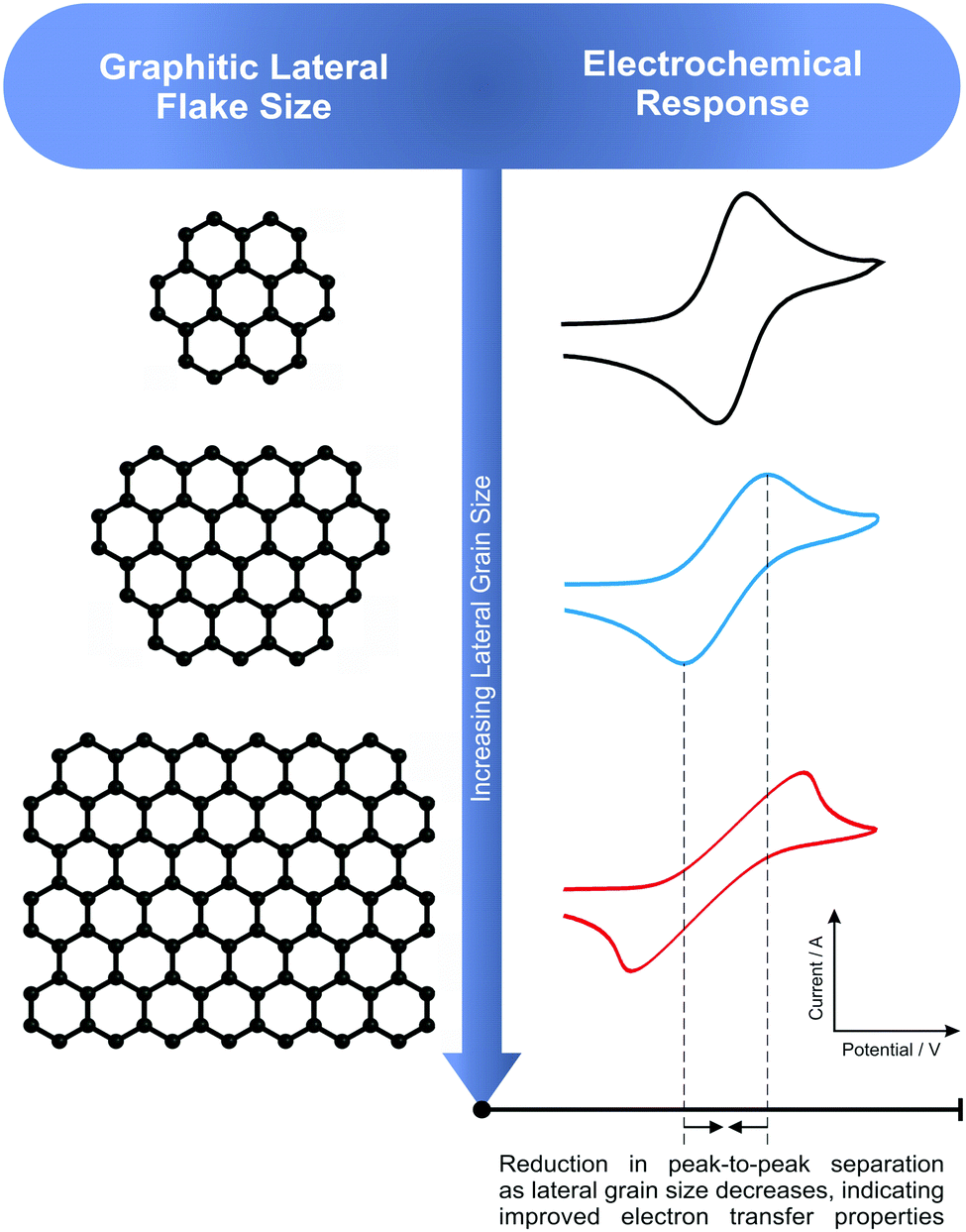 | ||
| Fig. 4 A schematic depicting the trends observed and reported herein. It is evident that, as the graphitic lateral flake size (La) decreases, an increase in electrochemical reactivity is observed, with increases noted in k0 values obtained and a reduction in the ΔEP. | ||
Electrostatic potential maps (ESP) of graphene
The calculation of atomic charges has a great impact on predicting the electronic properties and reactivity of molecules.62 From the atomic charges of a molecule, the software can predict the distribution of the electrostatic potential energy on the whole molecule to build up an image known as the electrostatic potential map (ESP). The electrostatic potential energy is maximum (high relative positive charge) where the colour of the ESP is deep blue. However, a red colour indicates the minimum electrostatic potential energy (high relative negative charge). ESPs are related to the electronic density of molecules and they can give information about the concentration of the electrons on the molecular structure.63 The ESPs herein were built using graphene sheets with different lateral flake sizes and the level of theory used in geometry optimisation (B3LYP/6-31G**) to investigate the influence of lateral flake size on the electronic density and HET. A frequency calculation was carried out (using the same functional) for all of the studied structures and no imaginary frequencies were found, indicating the stability of the illustrated geometries. The selected sizes of the models utilised are consistent with previous research articles concerning graphene materials modelling and in some cases our models are larger and more representative.79In Fig. 5, which depicts the ESPs, the orange colour indicates a low electrostatic potential, while the blue colour indicates a high electrostatic potential. The ESPs of the studied graphene flakes (2 × 3, 3 × 5 and 6 × 11 (ring × row)) depicts that the orange colour is concentrated in the central region of the flake as the flake's lateral size decreased. Consequently, the central carbon atoms of the 2 × 3 and 3 × 5 flakes possessed high electronic clouds. The electronic cloud (i.e. low electrostatic potential) is directed toward the lateral edge plane region in the 6 × 11 graphene flake. As a result, the electron-transfer process occurs in the central region (i.e. large area) in small graphene flakes rather than at the edges as per in the larger ones. These results, regarding the basal/edge plane electron transfer, are in agreement with previously published work.80–82
 | ||
| Fig. 5 DFT calculations on graphene flakes of different lateral flake size. (a–c) optimized geometry, (d–f) HOMO, (g–i) LUMO and (j–l) ESPs of 2 × 3, 3 × 5 and 6 × 11 (ring × row) flakes, respectively. The method of calculation used herein is B3LYP/6-31G** and the isovalue for FMOs and ESPs is 0.02. | ||
Frontier molecular orbitals (FMOs) of graphene
Frontier molecular orbitals (FMOs) result from the linear combination of the atomic orbitals of the atoms, of which the molecule is comprised. They have an important role in predicting the optical and electrical properties of the molecules.63 Moreover, FMOs are crucial in studying the electronic transitions and the transition states of molecules.62 In electronic transitions, HOMO represents the electron donor orbital and LUMO represents the electron acceptor orbital,64 and the FMOs of graphene flakes of varying sizes have different locations (Fig. 5d–i). As the size of the graphene flake decreases, the ratio of the edge plane region to the total flake size also decreases considerably. Consequently, FMOs reside in the central part of the small flake (e.g. 2 × 3 flake) enhancing the electron transfer, unlike the large flake (6 × 11) in which the FMOs reside in the lateral edges,80–82 hence hindering the electron transfer through the central region. However, in the 3 × 5 flake, homogeneous distribution of the FMOs was observed across the flake, which may suggest the highest electron transfer rate. In essence, in the case of the large graphene flake (6 × 11), the MOs span the edge regions of the molecule; then excitation of a HOMO electron into the LUMO would constitute a transfer of charge only through the edge plane. However, in case of 3 × 5 flakes, the MOs span almost the whole structure, which constitutes a spatial transfer of charge through the whole flake. The 2 × 3 flake is very small, so the distribution of the MOs is unique. It is obvious that the HOMO and LUMO of the 2 × 3 flake span the same region; therefore, the electrons are confined in the same place and no spatial transfer occurs. Based on these results, it can be inferred that there is an apparent threshold, in which a decrease in the lateral flake size leads to an increase in HET until the said threshold is reached and at this point, any further decrease in lateral flake size has no significant effect upon the electrochemical activity of the graphene flakes.Further studies were conducted on the density of states (DOS) of different graphene flakes (Fig. 6) as an attempt to correlate the obtained results with the previously calculated DOS diagrams for graphene materials. DOS is a concept of solid-state physics, which represents the number of electronic states per unit energy interval. The DOS of a given quantum system/material is a vital tool, utilised in order to understand the electrical conductivity and other electronic parametric responses.65 In all of the studied graphene flakes the conduction band was approximately below −5.0 eV while the valence band was almost at zero eV. The 3 × 5 and 6 × 11 graphene flakes showed some conductor metal-like characteristics. It was also observed that the electrical conductivity increased in the order (2 × 3) < (3 × 5) < (6 × 11). In fact, the 2 × 3 flake was more like an intrinsic semi-conductor with a band gap of 2.7 eV. Around the Fermi-level, all states comprise the p-orbitals of the carbons and only the s-orbitals contribute to energetically much lower and higher states.66 Furthermore, Van Hove singularities can be observed, possibly due to a peak in electrical resistance when the graphene is charge neutral or when graphene layers twist, leading to pronounced Van Hove singularities due to interlaying coupling.67 Accordingly, the observed changes in the DOS of different flake sizes suggests that there must be a change in the HET process. However, the challenge is how to explain the fact that the 6 × 11 graphene flake has the highest number of electronic states around the Fermi level, which may be erroneously interpreted as the highest conductivity. The electrical conductivity is not only dependent on the number of states around the Fermi level; this is only one of the many factors. It depends also on other properties, such as diffusion, band gap, the number of charge carriers and so on. Therefore, the apparent inconsistency of the electrical conductance of the 6 × 11 flake can be explained by the changes in these factors, which cannot be predicted using the DOS diagrams. From these results, it would seem that decreasing the lateral flake size below a certain extent (the aforementioned threshold size) causes a decrease in HET rates, therefore a decrease in the electrical conductivity was obtained in case of the 2 × 3 graphene flake. This corresponds well with previous literature; in which one study using computer simulations revealed that the DOS close to the Fermi level was independent of the electronic structure (i.e. triangular, hexagonal and round) in the case of graphene flakes, but was dependent on their size, especially in the case of hexagonal and round graphene flakes.68 Heiskanen et al., stated that this could possibly be due to their well-exhibited edge planes.68
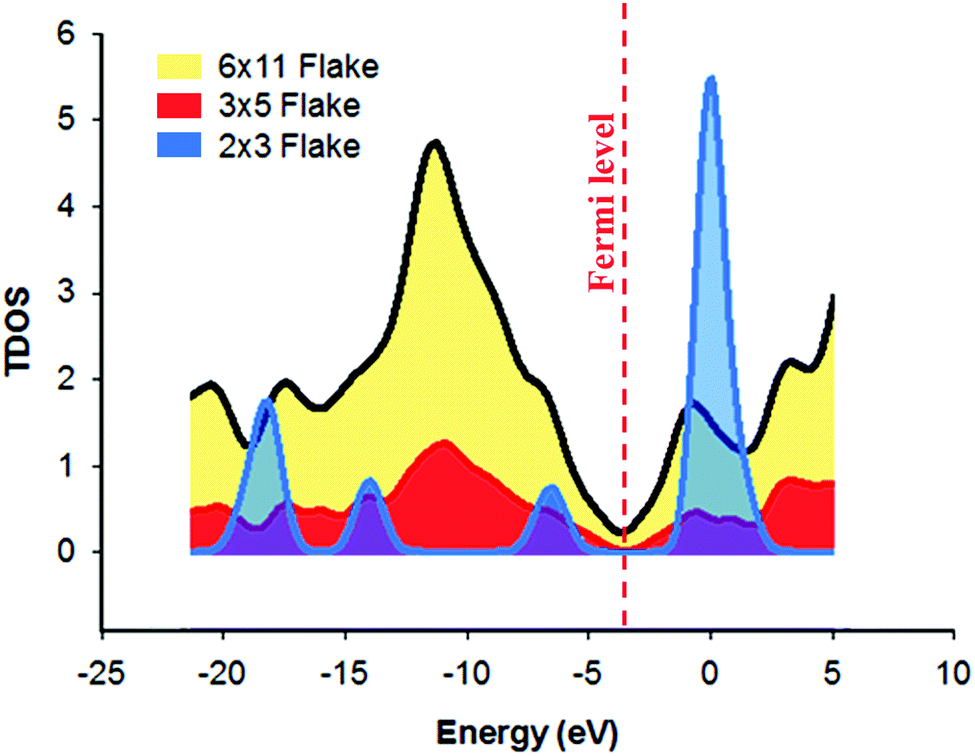 | ||
| Fig. 6 Total density of states (TDOS) of the investigated graphene flakes obtained from DFT calculations using the B3LYP/6-31G** functional. | ||
A summary of insights regarding the lateral flake size and resulting electrochemical properties at graphitic electrodes
A direct relationship has been observed with respect to the lateral flake size comprising graphene and graphite electrodes and their corresponding electron transfer properties, with smaller flake sizes (increased edge plane contributions) resulting in an improved electrochemical performance. When the graphite/graphene electrodes are explored towards outer-sphere redox probes (such as hexaammineruthenium(III) chloride) the aforementioned trend was clear, with the large lateral flake sizes demonstrating reduced performance and slower HET (k0) rates compared to their smaller lateral flake counterparts, which possessed higher % edge plane contributions and larger calculated/estimated reactive areas (Aeff). Such calculations are possible due to the nature of outer-sphere probe's electrochemical performance being dependent on the electronic structure of the electrode only (see ESI†). Interestingly, when inner-sphere redox probes are utilised, although similar trends are evident, there were specific cases where a material gave rise to an unexpected favourable/unfavourable electrochemical response. For example, flake graphite (one of the ‘larger’ lateral flake sizes) exhibited the fastest rate of electron transfer when measured using the potassium ferrocyanide(II) probe (Table 1). However, due to the intricate nature of inner-sphere probes and their increased sensitivity towards oxygenated species and ligands, the electrochemical reactivity is convoluted, with the resulting HET rates misinterpreted if the surface state is not considered accordingly given this high dependence upon the physical structure of the electrode surface.69Considering the observations using the outer-sphere redox probes, such that smaller lateral flake sizes gave rise to improved electrochemical properties, such as smaller ΔEP and larger k0 values. It is inferred that the higher global coverage of edge plane like-sites/defects arising due to the favourable edge plane to basal plane ratio enhances electrochemical performance. This supports previous literature which states that edge plane sites are the predominant origin of fast electron kinetics in graphitic materials, with comparably slow HET rates demonstrated by large films/flakes of pristine graphene likely a result of graphene's fundamental configuration; comprising a low edge plane to high basal plane ratio.8
Given that the density or % coverage of edge plane like-sites/defects on an electrode's surface plays a pivotal role in determining its electrochemical efficacy, this parameter needs to be investigated and optimised (flake thickness, lateral flake size, geometry, orientation, etc.) at carbon-based electrodes in order to achieve enhanced performance in numerous fields of application.70
Conclusions
We have shown, for the first time, utilising graphite and graphene based paste electrodes with varying lateral flake sizes, that the respective electrode's electrochemical reactivity depends directly on its structural composition. Decreasing the lateral flake sizes at graphitic electrodes resulted in improved electrochemical performances, with faster HET evident in such cases. These findings are attributed to the resulting percentage of ‘edge-to-basal plane ratio’ on the various flakes, with a reduction in lateral flake size correlating to a distinct increase in the number (or % composition) of edge plane area/sites present on the electrode surface. As such, we infer that the observed improvement in electrochemical activity in such cases (when using outer-sphere redox probes) is directly related to the edge plane content and hence the lateral flake size when using graphitic based electrodes. Interestingly, specifically when using the graphene electrodes (with the smallest lateral flake sizes), the above trend was evident up to a specific point, termed the ‘lateral size threshold’, after which the improvement/increment in the amount of edge planes available to partake in HET became such that no (further) vast improvement was seen in the electrochemical activity given that the process was close to the reversible limit. Inner-sphere redox probes were also utilised and similar underlying trends were present, however, the graphite electrodes were highly sensitive to the redox probe due to oxygenated species (and ligands) and as such, in some instances where favourable surface groups interacted with the probe being studied, the general trend relating to the edge plane density was perturbed.The above conclusions are supported by DFT calculations, which have revealed that in smaller graphene lateral flake sizes (2 × 3 and 3 × 5 carbon atoms), electron transfer processes occur in the central region of the flake as opposed to larger flakes (6 × 11 carbon atoms) where the outer regions (i.e. edge planes) demonstrate low electrostatic potential. These results concur with the electrochemical analysis of the graphite and graphene of varying lateral flake sizes, providing evidence that one will observe an increase in electrochemical reactivity as the lateral flake size is reduced, theoretically and/or possibly up to the ‘lateral size threshold’ (a critical value/limit), where afterwards the reversible limit of the electrochemistry is achieved and/or the entire flake becomes reactive such that electron transfer will remain unaltered.
This work highlights the importance of considering the lateral flake size when selecting materials to be implemented as electrodes with improved/fast HET and favourable electrochemical responses. Given the insights gained herein, novel materials (i.e. 2D-nanomaterials) selected for potential electrode development should have a higher edge plane density, leading to increased HET rates where required. Future research needs to focus on optimising such flake sizes in carbonaceous electrode materials for applications such as energy storage and sensors.
Conflicts of interest
There are no conflicts to declare.Acknowledgements
The authors acknowledge a British Council Institutional Link grant (No. 172726574) for the support of this research. D. A. C. Brownson acknowledges funding from the Ramsay Memorial Fellowships Trust.References
- R. N. Adams, Anal. Chem., 1958, 30, 1576 CrossRef.
- L. C. S. Figueiredo-Filho, D. A. C. Brownson, M. Gomez-Mingot, J. Iniesta, O. Fatibello-Filho and C. E. Banks, Analyst, 2013, 138, 6354–6364 RSC.
- D. A. C. Brownson and C. E. Banks, The handbook of graphene electrochemistry, Springer, London, 2014 Search PubMed.
- A. Bianco, H.-M. Cheng, T. Enoki, Y. Gogotsi, R. H. Hurt, N. Koratkar, T. Kyotani, M. Monthioux, C. R. Park, J. M. D. Tascon and J. Zhang, Carbon, 2013, 65, 1–6 CrossRef.
- D. A. C. Brownson, D. K. Kampouris and C. E. Banks, Chem. Soc. Rev., 2012, 41, 6944–6976 RSC.
- R. F. Service, Science, 2009, 324, 875–877 CrossRef PubMed.
- Y. Shao, J. Wang, H. Wu, J. Liu, I. A. Aksay and Y. Lin, Electroanalysis, 2010, 22, 1027–1036 CrossRef.
- D. A. C. Brownson, S. A. Varey, F. Hussain, S. J. Haigh and C. E. Banks, Nanoscale, 2014, 6, 1607–1621 RSC.
- W. Li, C. Tan, M. A. Lowe, H. D. Abruña and D. C. Ralph, ACS Nano, 2011, 5, 2264–2270 CrossRef PubMed.
- A. T. Valota, I. A. Kinloch, K. S. Novoselov, C. Casiraghi, A. Eckmann, E. W. Hill and R. A. W. Dryfe, ACS Nano, 2011, 5, 8809–8815 CrossRef PubMed.
- W. Yuan, Y. Zhou, Y. Li, C. Li, H. Peng, J. Zhang, Z. Liu, L. Dai and G. Shi, Sci. Rep., 2013, 3 Search PubMed.
- R. L. McCreery, Chem. Rev., 2008, 108, 2646–2687 CrossRef PubMed.
- C. Neumann, C. Batchelor-McAuley, C. Downing and R. G. Compton, Chem. – Eur. J., 2011, 17, 7320–7326 CrossRef PubMed.
- S. J. Rowley-Neale, D. A. C. Brownson and C. E. Banks, Nanoscale, 2016, 8, 15241–15251 RSC.
- T. J. Davies, M. E. Hyde and R. G. Compton, Angew. Chem., Int. Ed. Engl., 2005, 44, 5121–5126 CrossRef PubMed.
- C. E. Banks, T. J. Davies, G. G. Wildgoose and R. G. Compton, Chem. Commun., 2005, 829–841 RSC.
- D. A. C. Brownson, L. C. S. Figueiredo-Filho, X. Ji, M. Gomez-Mingot, J. Iniesta, O. Fatibello-Filho, D. K. Kampouris and C. E. Banks, J. Mater. Chem. A, 2013, 1, 5962–5972 RSC.
- D. A. C. Brownson, R. V. Gorbachev, S. J. Haigh and C. E. Banks, Analyst, 2012, 137, 833–839 RSC.
- L. C. Figueiredo-Filho, D. A. C. Brownson, O. Fatibello-Filho and C. E. Banks, Analyst, 2013, 138, 4436–4442 RSC.
- C. Li and G. Shi, Nanoscale, 2012, 4, 5549–5563 RSC.
- C. W. Foster, M. P. Down, Y. Zhang, X. Ji, S. J. Rowley-Neale, G. C. Smith, P. J. Kelly and C. E. Banks, Sci. Rep., 2017, 7, 42233 CrossRef PubMed.
- C. Zhu, T. Y.-J. Han, E. B. Duoss, A. M. Golobic, J. D. Kuntz, C. M. Spadaccini and M. A. Worsley, Nat. Commun., 2015, 6, 6962 CrossRef PubMed.
- A. E. Jakus, E. B. Secor, A. L. Rutz, S. W. Jordan, M. C. Hersam and R. N. Shah, ACS Nano, 2015, 9, 4636–4648 CrossRef PubMed.
- M. H. Parvin, Electrochem. Commun., 2011, 13, 366–369 CrossRef.
- Y. Bo, W. Wang, J. Qi and S. Huang, Analyst, 2011, 136, 1946–1951 RSC.
- A. Gasnier, M. L. Pedano, M. D. Rubianes and G. A. Rivas, Sens. Actuators, B, 2013, 176, 921–926 CrossRef.
- F. Li, J. Li, Y. Feng, L. Yang and Z. Du, Sens. Actuators, B, 2011, 157, 110–114 CrossRef.
- K.-J. Huang, J. Li, Y.-M. Liu, X. Cao, S. Yu and M. Yu, Microchim. Acta, 2012, 177, 419–426 CrossRef.
- G. Supermarket, https://graphene-supermarket.com/home.php, accessed 3/10/17.
- D. A. C. Brownson, L. C. S. Figueiredo-Filho, B. L. Riehl, B. D. Riehl, M. Gomez-Mingot, J. Iniesta, O. Fatibello-Filho and C. E. Banks, J. Mater. Chem. A, 2016, 4, 2617–2629 RSC.
- E. P. Randviir, D. A. C. Brownson, J. P. Metters, R. O. Kadara and C. E. Banks, Phys. Chem. Chem. Phys., 2014, 16, 4598–4611 RSC.
- S. J. Rowley-Neale, D. A. C. Brownson, G. C. Smith, D. A. G. Sawtell, P. J. Kelly and C. E. Banks, Nanoscale, 2015, 7, 18152–18168 RSC.
- R. S. Nicholson, Anal. Chem., 1965, 37, 1351–1355 CrossRef.
- J. P. Metters, S. M. Houssein, D. K. Kampouris and C. E. Banks, Anal. Methods, 2013, 5, 103–110 RSC.
- L. R. Cumba, C. W. Foster, D. A. C. Brownson, J. P. Smith, J. Iniesta, B. Thakur, D. R. do Carmo and C. E. Banks, Analyst, 2016, 141, 2791–2799 RSC.
- I. Lavagnini, R. Antiochia and F. Magno, Electroanalysis, 2004, 16, 505–506 CrossRef.
- C. E. Banks, R. G. Compton, A. C. Fisher and I. E. Henley, Phys. Chem. Chem. Phys., 2004, 6, 3147–3152 RSC.
- Y. S. Grewal, M. J. A. Shiddiky, S. A. Gray, K. M. Weigel, G. A. Cangelosi and M. Trau, Chem. Commun., 2013, 49, 1551–1553 RSC.
- C. W. Foster, D. A. C. Brownson, A. P. Ruas de Souza, E. Bernalte, J. Iniesta, M. Bertotti and C. E. Banks, Analyst, 2016, 141, 4055–4064 RSC.
- M. J. Moorcroft, N. S. Lawrence, B. A. Coles, R. G. Compton and L. N. Trevani, J. Electroanal. Chem., 2001, 506, 28–33 CrossRef.
- E. Blanco, C. W. Foster, L. R. Cumba, D. R. do Carmo and C. E. Banks, Analyst, 2016, 141, 2783–2790 RSC.
- S. J. Rowley-Neale, C. W. Foster, G. C. Smith, D. A. C. Brownson and C. E. Banks, Sustainable Energy Fuels, 2017, 1, 74–83 RSC.
- S. Shin, Z. Jin, D. H. Kwon, R. Bose and Y.-S. Min, Langmuir, 2015, 31, 1196–1202 CrossRef PubMed.
- R. E. G. Smith, T. J. Davies, N. d. B. Baynes and R. J. Nichols, J. Electroanal. Chem., 2015, 747, 29–38 CrossRef.
- J. Ortiz, J. Cioslowski and D. Fox, Gaussian 09, Gaussian, Inc., Wallingford, CT, 2009 Search PubMed.
- W. M. Hassan and A. S. Abo Dena, Anal. Chem., 2014, 86, 1881–1886 CrossRef PubMed.
- C. Lee, W. Yang and R. G. Parr, Phys. Rev. B: Condens. Matter Mater. Phys., 1988, 37, 785 CrossRef.
- R. Ditchfield, W. J. Hehre and J. A. Pople, J. Chem. Phys., 1971, 54, 724–728 CrossRef.
- R. Ditchfield, Mol. Phys., 1974, 27, 789–807 CrossRef.
- K. D. Dobbs and W. Hehre, J. Comput. Chem., 1986, 7, 359–378 CrossRef.
- K. D. Dobbs and W. Hehre, J. Comput. Chem., 1987, 8, 861–879 CrossRef.
- K. D. Dobbs and W. Hehre, J. Comput. Chem., 1987, 8, 880–893 CrossRef.
- R. Dennington, T. Keith and J. Millam, GaussView Version 05, 2009 Search PubMed.
- R. L. McCreery, Chem. Rev., 2008, 108, 2646–2687 CrossRef PubMed.
- A. C. Ferrari, Solid State Commun., 2007, 143, 47–57 CrossRef.
- D. Graf, F. Molitor, K. Ensslin, C. Stampfer, A. Jungen, C. Hierold and L. Wirtz, Nano Lett., 2007, 7, 238–242 CrossRef PubMed.
- Y. Y. Wang, Z. H. Ni, T. Yu, Z. X. Shen, H. M. Wang, Y. H. Wu, W. Chen and A. T. Shen Wee, J. Phys. Chem. C, 2008, 112, 10637–10640 CrossRef.
- D. Yoon, H. Moon, H. Cheong, J. S. Choi, J. A. Choi and B. H. Park, J. Korean Phys. Soc., 2009, 55, 1299–1303 CrossRef.
- P. Chen and R. L. McCreery, Anal. Chem., 1996, 68, 3958–3965 CrossRef.
- M. R. Kagan and R. L. McCreery, Langmuir, 1995, 11, 4041–4047 CrossRef.
- A. D. Clegg, N. V. Rees, O. V. Klymenko, B. A. Coles and R. G. Compton, J. Am. Chem. Soc., 2004, 126, 6185–6192 CrossRef PubMed.
- A. S. A. Dena and W. M. Hassan, Spectrochim. Acta, Part A, 2016, 163, 108–114 CrossRef PubMed.
- A. M. Mansour, H. M. Hassaneen, Y. S. Mohammed and N. T. A. Ghani, J. Mol. Struct., 2013, 1045, 180–190 CrossRef.
- A. S. Dena and W. M. Hassan, Spectrochim. Acta, Part A, 2016, 163, 108–114 CrossRef PubMed.
- S. Dröscher, P. Roulleau, F. Molitor, P. Studerus, C. Stampfer, K. Ensslin and T. Ihn, Appl. Phys. Lett., 2010, 96, 152104 CrossRef.
- K. Nakada, M. Fujita, G. Dresselhaus and M. S. Dresselhaus, Phys. Rev. B: Condens. Matter Mater. Phys., 1996, 54, 17954 CrossRef.
- L. Van Hove, Phys. Rev., 1953, 89, 1189–1193 CrossRef.
- H. Heiskanen, M. Manninen and J. Akola, New J. Phys., 2008, 10, 103015 CrossRef.
- S. Tanimoto and A. Ichimura, J. Chem. Educ., 2013, 90, 778–781 CrossRef.
- L. Hu, X. Peng, K. Huo, R. Chen, J. Fu, Y. Li, L. Y. S. Lee, K.-Y. Wong and P. K. Chu, ACS Appl. Mater. Interfaces, 2016, 8, 28872–28879 CrossRef PubMed.
- A. F. Khan, D. A. C. Brownson, C. W. Foster, G. C. Smith and C. E. Banks, Analyst, 2017, 142, 1756–1764 RSC.
- D. A. C. Brownson and C. E. Banks, Analyst, 2011, 136, 2084–2089 RSC.
- R. M. A. Edwards, P. Bertoncello and P. R. Unwin, J. Phys. Chem. C, 2009, 113, 9218–9223 CrossRef.
- D. A. C. Brownson, G. C. Smith and C. E. Banks, R. Soc. Open Sci., 2017, 4, 171128 CrossRef PubMed.
- A. G.-M. Ferrari, C. W. Foster, P. J. Kelly, D. A. C. Brownson and C. E. Banks, Biosensors, 2018, 8, 53 CrossRef PubMed.
- W. Song, X. Ji, W. Deng, Q. Chen, C. Shen and C. E. Banks, Phys. Chem. Chem. Phys., 2013, 15, 4799 RSC.
- D. A. C. Brownson and C. E. Banks, Chem. Commun., 2012, 48, 1425 RSC.
- W. Deng, X. Ji, M. Gómez-Mingot, F. Lu, Q. Chen and C. E. Banks, Chem. Commun., 2012, 48, 2770 RSC.
- D. A. C. Brownson, L. J. Munro, D. K. Kampouris and C. E. Banks, RSC Adv., 2011, 1, 978–988 RSC.
- D. K. Kampouris and C. E. Banks, Chem. Commun., 2010, 46, 8986–8988 RSC.
- X. Ji, C. E. Banks, A. Crossley and R. G. Compton, ChemPhysChem, 2006, 7, 1337–1344 CrossRef PubMed.
- W. Yuan, Y. Zhou, Y. Li, C. Li, H. Peng, J. Zhang, Z. Liu, L. Dai and G. Shi, Sci. Rep., 2013, 3, 1–7 Search PubMed.
Footnote |
| † Electronic supplementary information (ESI) available. See DOI: 10.1039/c8cp02196a |
| This journal is © the Owner Societies 2018 |