
 Open Access Article
 This Open Access Article is licensed under a
 Creative Commons Attribution 3.0 Unported Licence
Oxide–organic heterostructures: a case study of charge transfer disturbance at a SnO2–copper phthalocyanine buried interface
Maciej
Krzywiecki
 *ab,
Lucyna
Grządziel
b,
Paulina
Powroźnik
b,
Monika
Kwoka
c,
Julian
Rechmann
a and
Andreas
Erbe
ad
*ab,
Lucyna
Grządziel
b,
Paulina
Powroźnik
b,
Monika
Kwoka
c,
Julian
Rechmann
a and
Andreas
Erbe
ad
aMax-Planck-Institut für Eisenforschung GmbH, Max-Planck-Str. 1, 40237 Düsseldorf, Germany. E-mail: Maciej.Krzywiecki@polsl.pl; Fax: +48 (32) 237 22 16; Tel: +48 (32) 237 20 01
bInstitute of Physics – Center for Science and Education, Silesian University of Technology, S. Konarskiego 22B, 44-100 Gliwice, Poland
cInstitute of Electronics, Silesian University of Technology, Akademicka 16, 44-100 Gliwice, Poland
dDepartment of Materials Science and Engineering, NTNU, Norwegian University of Science and Technology, 7491 Trondheim, Norway
First published on 18th May 2018
Abstract
Reduced tin dioxide/copper phthalocyanine (SnOx/CuPc) heterojunctions recently gained much attention in hybrid electronics due to their defect structure, allowing tuning of the electronic properties at the interface towards particular needs. In this work, we focus on the creation and analysis of the interface between the oxide and organic layer. The inorganic/organic heterojunction was created by depositing CuPc on SnOx layers prepared with the rheotaxial growth and vacuum oxidation (RGVO) method. Exploiting surface sensitive photoelectron spectroscopy techniques, angle dependent X-ray and UV photoelectron spectroscopy (ADXPS and UPS, respectively), supported by semi-empirical simulations, the role of carbon from adventitious organic adsorbates directly at the SnOx/CuPc interface was investigated. The adventitious organic adsorbates were blocking electronic interactions between the environment and surface, hence pinning energy levels. A significant interface dipole of 0.4 eV was detected, compensating for the difference in work functions of the materials in contact, however, without full alignment of the energy levels. From the ADXPS and UPS results, a detailed diagram of the interfacial electronic structure was constructed, giving insight into how to tailor SnOx/CuPc heterojunctions towards specific applications. On the one hand, parasitic surface contamination could be utilized in technology for passivation-like processes. On the other hand, if one needs to keep the oxide's surficial interactions fully accessible, like in the case of stacked electronic systems or gas sensor applications, carbon contamination must be carefully avoided at each processing step.
Introduction
Hybrid heterojunctions created out of inorganic–organic material stacks are currently attracting more and more attention due to the number of technological applications.1–3 Especially low-dimensional heterostructures with applications varying from photovoltaics4,5 through other optoelectronic and thermoelectronic devices6–8 to inorganic–organic transistors9 are at the center of interest.The device performance is tightly linked to the electronic and chemical properties of the interface between the materials in the junction.10,11 These properties in turn are strongly defined by the physical and chemical phenomena affecting charge carrier transfer, energy level alignment, or the oxidation state of a component of the particular constituents at the buried heterojunction. Last but not least, interstitial constituents located e.g. between the organic and the inorganic part can act as dopants or contaminants at the interface. In the case of ultra-thin layers with a Debye screening length on the order of the layer thickness, the bulk is in fact the subsurface. Consequently, a careful description is becoming even more important, leaving no option for particular effects of bulk relaxation. Hence, a thorough understanding of the processes at the interface becomes crucial for optimal heterostructure performance as well as for quality and efficiency of electronic device operation.12
Characterization of a number of systems has been lately presented in the field of hybrid materials,13,14 highlighting the need to carefully control several aspects of the interface structure in order to obtain junctions of desired properties. Among these aspects are (i) interface controlled stoichiometry,15 (ii) morphology including lattice mismatch,16 (iii) impurities and contamination impact17 and (iv) energy level alignment controlling undisturbed charge transfer.17 Most of the issues can be controlled by selecting an appropriately advanced preparation technique. However, sophisticated methods, such as molecular beam epitaxy or atomic layer deposition, are in the majority less time- and cost-efficient.18 Therefore, careful characterization is required to select the most efficient combination of preparation methods and processing procedures, resulting in more efficient devices with regard to both performance and economy.
Among hybrid materials, the inorganic–organic heterojunctions based on tin oxides and metallophthalocyanines (MePc) have attracted attention recently as being promising in a number of applications.19,20 Tin oxides are wide-band gap transparent oxides in which the deviation from the stoichiometric composition as well as the presence of additional defects and impurities creates intra-bandgap states modifying the oxide electronic structure. Hence, the oxide electronic structure can be tailored towards particular needs.21 In this work, we will refer to SnO1<x<2 as reduced tin dioxide. MePcs are molecular semiconductors of high chemical stability.22 An easily accessible promising representative of MePcs is copper phthalocyanine (CuPc), which is now becoming a popular organometallic compound already applied in third generation solar cells, gas sensors and advanced optoelectronic technologies.23–25
Up to now, the majority of studies were oriented towards various modifications of the tin oxide,26 leaving the interfacial area unattended. There are only a few studies reporting thorough characterization of both the interfacial area and the processes taking place there.27 The mainstream approach to buried interface investigation is to use a step-by-step deposition with succeeding investigation,28 demanding complicated experimental setups, or destructive ion-etching assisted probing.29 Some work also incorporates expensive synchrotron radiation-based photoelectron spectroscopy experiments,30 which are very accurate but have limited accessibility. An alternative is an angle dependent photoemission experiment, allowing the use of lab-based equipment for non-destructive in situ and post process examinations. The most important advantage of this method is the extremely low influence of the probing medium on the structure being probed.31
Angle dependent X-ray photoelectron spectroscopy (ADXPS) was used in our former studies on ultra-thin tin oxides.32 In the current work, we present photoemission-based studies on the interface between SnO1<x<2 layers obtained by the rheotaxial growth and vacuum oxidation (RGVO) technique, hereafter called RGVO–SnOx, and CuPc ultrathin films deposited by physical vapor deposition (PVD). RGVO was chosen because of its unique possibility for stoichiometry control with relatively low cost in comparison to other vacuum-based techniques like e.g. molecular beam epitaxy. The method results in samples of high purity while kept in vacuum.33
Due to the dual, energy-resolved analytical approach i.e. combining depth resolution of ADXPS and surface sensitivity of ultraviolet photoelectron spectroscopy (UPS), a non-destructive analysis of the energy level positioning was performed.
Because of the perspective of SnOx/CuPc heterojunction application in hybrid electronics, we focus on the creation and analysis of the interface between the oxide and organic layer.
Experimental details
As a substrate for sample preparation, commercially available silicon Si(100) wafers were used (Bosch GmbH, n-type, p-doped, 5–10 Ω cm). Prior to further processing, substrates were cleaned sequentially in an ultrasonic bath in acetone and isopropanol for 15 min in each solvent, then rinsed with de-ionized water (<10 μS conductivity) and blown with a dry stream of nitrogen and annealed for 30 min in an oven at 110 °C.RGVO–SnOx layers were deposited on Si substrates in an ultrahigh vacuum (UHV) system of base pressure 3 × 10⁻⁹ mbar.33 The method utilizes the thermal evaporation of Sn pellets (KJLC®) from a resistively heated source. During evaporation, substrates were kept at 265 °C and the oxygen partial pressure was kept at 10−4 mbar. The resulting layers were 20 nm thick as controlled with an Inficon XTC3M quartz crystal microbalance (QCM). The final stoichiometry tuning was performed by additional in situ vacuum oxidation at an oxygen exposure of 108 L. For both steps of exposure, pure oxygen (Messer CanGas; 5.0 purity) was used.
CuPc ultra-thin films were deposited on RGVO–SnOx layers by PVD in a separate UHV system (base pressure <5 × 10⁻⁹ mbar). The CuPc powder (Sigma-Aldrich, 99.7% dye content) was degassed and purified in UHV by keeping the effusion cell at 240 °C for 5 h prior to the deposition. During the evaporation process, the layer growth was controlled by QCM (PREVAC TMC-13). The evaporation rate was kept at the level of 0.1 Å s−1 to provide uniform CuPc films, thus creating RGVO–SnOx/CuPc samples.
The ADXPS measurements were done with a Physical Electronics PHI Quantera II spectrometer equipped with an Al-Kα micro-focused source (1486.6 eV; spot diameter <100 μm) assisted by a dual-beam charge neutralization system, working at a base pressure of <1 × 10⁻⁹ mbar.
The survey spectra were recorded with the pass energy set to 140 eV and an energy step of 0.4 eV. The high-resolution core level energy regions were recorded with a pass energy of 26 eV and an energy step of 0.025 eV. All XPS spectra were recorded with a take-off angle (TOA - defined as an angle between the analyzer axis and the sample's surface plane) varying from 90° to 20°. The analyzer acceptance angle was limited to ±4° to increase angular sensitivity.
ADXPS data were analyzed by curve fitting using the CASA XPS software.34 If not specified, peaks were represented by a convolution of Gaussian (70%) and Lorentzian (30%) lines, and the secondary electron background was processed with the Shirley function. The lowest number of components was used. The estimated uncertainty for a particular component energy position was 0.04 eV. The quantitative analysis was done using CASA XPS embedded relative sensitivity factors (RSF) and algorithms. The Au 4f7/2 (84.0 eV)35 region recorded for a gold-covered sample placed at the same sample holder was utilized for binding energy (B.E.) scale calibration.
The information depth estimation was performed with procedures described in our previous study32 and is based on the algorithm described by R. L. Opila and J. Eng Jr.36 The procedure is also provided by a leading equipment manufacturer.37 Simplified, the intensity I of the detected photoelectron signal is dependent on the information depth d, following the relation36
I = I0 ![[thin space (1/6-em)]](https://www.rsc.org/images/entities/char_2009.gif) exp(−d/λcosθ), exp(−d/λcosθ), |
Here, an information depth of 0 nm was ascribed to the RGVO–SnOx/CuPc interface. The information depth analysis was done with assumptions that photoelectron attenuation length λa = λ; approximately 65% of the photoelectron signal comes from the depth equal to λ, and λa is constant within the examined layer.38 Further assumptions can be found elsewhere.32 The required λa and inelastic mean free path (IMFP) parameters were determined from the NIST electron inelastic mean free path database and electron attenuation length calculating software,39 which utilizes algorithms based on the analysis proposed by Werner,40 and applying the TPP-2M (Tanuma–Powell–Penn)41 algorithm. For the substrate Sn 3d peak under the CuPc organic film, λa was estimated as 2.54(15) nm. The total thickness of the CuPc layer was determined as 2.60(25) nm with an analysis procedure originally proposed by Cumpson.42 This value is quite close to the indications of the QCM (3.00 nm).
Constituent positioning within the examined system was done utilizing ADXPS-based relative depth plot (RDP) analysis.43 This plot allows positioning of the elements or particular components of peaks, included in stacked layered samples with respect to the bulk or to their surface. Although the method is not giving the actual depth of a particular component, it is able to indicate a component's depth compared to other components. The relative depth drel is obtained from comparing intensities I at different TOAs as a plot connected to the component's average depth following the relation:44,45
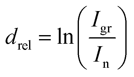 | (1) |
UPS measurements were performed with a PREVAC EA15 hemispherical electron energy analyzer equipped with a 2D multi-channel plate detector. The excitation was provided by a PREVAC UVS-40A2 helium discharge lamp providing UV radiation of energy 21.22 eV (He I line).
The provided uncertainties within this work were calculated with use of the standard uncertainty propagation methods which can be found in the literature.46 The uncertainty analysis accounted for photoemission peak angular broadening and charging effects as well as random errors which could occur during the experiment.47,48
For theoretical augmentation of charge transfer detection between oxide and CuPc layers semi-empirical calculations were performed utilizing SCIGRESS® software, version FJ 2.8 (EU 3. 2. 2, copyright 2008–2017 FUJITSU LIMITED). As a result, Mulliken partial charges were calculated with the MO–G calculation modules using parametric method 6 (PM6) for solving the Schrödinger equation. To simulate RGVO–SnOx layers, the cluster approach was applied for simplification of the modeling procedure. It utilized Sn3O4(OH)4 clusters for SnO2 (1 0 0) surface modeling.49–52 All of the initial cluster structures were saturated with hydrogen atoms and optimized based on SCIGRESS® optimization algorithms.53 In order to obtain the lowest energy conformations of Sn3O4(OH)4/CuPc and Sn3O4(CH3)4/CuPc, the potential energy maps of initial structures have been determined by the molecular mechanics method MM2. Calculations have been carried out using the Cu–Sn distance as a search label, in the range of 1–5 Å in 50 steps of 0.08 Å. A full geometry optimization with the PM6 method has been performed for the lowest energy conformations (1.8 Å distance between the SnO cluster and CuPc for Sn3O4(OH)4/CuPc and 2.2 Å for Sn3O4(OCH3)4/CuPc).
Results and discussion
The chemical composition of the prepared RGVO–SnOx and their CuPc-covered analogues was monitored on the basis of the Sn 3d, O 1s and C 1s energy regions with XPS. For CuPc-covered samples, the N 1s energy region was additionally examined. Respective data recorded for TOA = 90° are presented in Fig. 1(a–c) for RGVO–SnOx, and Fig. 1(d–g) for CuPc – covered samples. | ||
| Fig. 1 Representative XPS regions recorded for bare RGVo–SnOx (a–c) and for RGVO–SnOx/CuPc (d–g). ‘sat’ components represent the satellite features with the subscript determining their main peak. All presented regions were recorded at TOA = 90°. Lines represent the fits. The purple line stands for the Shirley-type background. | ||
The RGVO–SnOx layers showed only minor oxygen-related contamination [Ocont. in Fig. 1(b)] represented by a small component at the high binding energy scale side with respect to the main O–Sn component.54 Based on the lower than moderate carbon contamination (Fig. 1(c)), this component in the O 1s region is most likely organically bound oxygen, such as C–O/C![[double bond, length as m-dash]](https://www.rsc.org/images/entities/char_e001.gif) O. Contamination is most likely related to post deposition adsorption of water and organic adsorbates, as observed in former experiments.33 To enable an intensity comparison, the C 1s region for the CuPc-covered sample (Fig. 1(d)) is depicted on the same intensity scale as for the bare sample.
O. Contamination is most likely related to post deposition adsorption of water and organic adsorbates, as observed in former experiments.33 To enable an intensity comparison, the C 1s region for the CuPc-covered sample (Fig. 1(d)) is depicted on the same intensity scale as for the bare sample.
The C 1s decomposition yielded the expected result for CuPc components, i.e. C–C and C–N together with their satellites in the expected intensity ratios, and with the shape reproducing the classical shape for thick CuPc layers.55 The ultimate ∼3 nm layer thickness allowed tracking of the behavior of both substrate-originating and CuPc-originating components with the ADXPS method. This particular thickness assures also that all of the important interface-related phenomena, i.e. the interfacial dipole effect and the band bending-like impact along this region can be revealed due to fact that 3 nm thick CuPc layers are usually continuous and well-ordered.56
The contamination signal originating from the oxide underneath is still detectable with minor intensity as represented by relatively broad component Ccont. The only additional contamination was detected in the O 1s energy region (Fig. 1(f) – marked as Ocont.), as was indicated by the significant increase of the Ocont./O–Sn intensity ratio. This contamination can be related as well to environment–CuPc layer interaction which was previously observed for similar systems.55,57 The minor component at the high-binding energy side can be related to a trace amount of organic contamination, adsorbed water vapor55 and/or to an energy-loss satellite feature. Interestingly, there is no significant contamination that would show up in the C 1s or N 1s regions of the CuPc layer, indicating an absence of organic N-containing contaminating organic adsorbates.
Although the component assignment was done on the basis of the available literature and databases,58 there is still room for possible data misinterpretation. Therefore, to evaluate the above assignment about the contaminating adsorbate origin and to check the layer ordering, a RDP analysis was performed. The resulting RDP is depicted in Fig. 2. The calculations, based on ADXPS results, were done for the main detected components relevant in the present study. These are the Sn–O, Ccont, O–Sn and Ocont. components for the RGVO–SnOx samples, and the C–C, C–N, Sn–O, Ccont, O–Sn, Ocont and N–C for the RGVO–SnOx/CuPc samples. The notation of the components is such that it gives the main energy region where they were detected first, e.g., N–C originates from N 1s while C–N from the C 1s region.
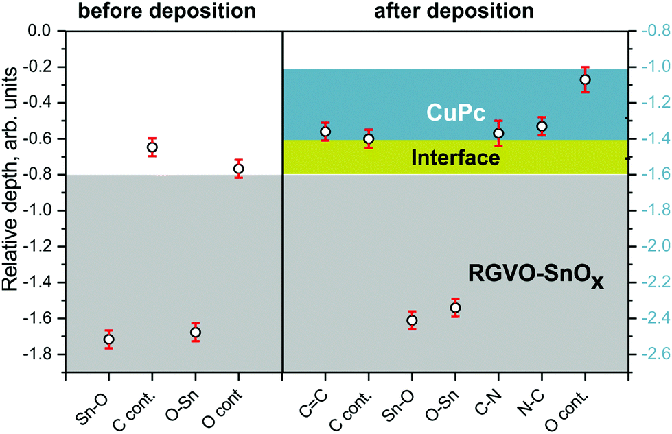 | ||
Fig. 2 Relative depth plot for RGVO–SnOx samples before deposition (left) and after CuPc deposition (right side). The cyan ( ) area represents the CuPc layer and the gray ( ) area represents the CuPc layer and the gray ( ) area depicts the RGVO–SnOx layer. The Y-axis scale presents the relative depth position scale of the respective component (the left scale corresponds to the bare oxide system while the right one to the CuPc covered stack). The dark yellow stripe between cyan and gray areas in the right part of the diagram stands for the RGVO–SnOx/CuPc interface. ) area depicts the RGVO–SnOx layer. The Y-axis scale presents the relative depth position scale of the respective component (the left scale corresponds to the bare oxide system while the right one to the CuPc covered stack). The dark yellow stripe between cyan and gray areas in the right part of the diagram stands for the RGVO–SnOx/CuPc interface. | ||
For the bare oxide layer, an evident difference was detected between the relative position of SnOx-related components Sn–O and O–Sn, and contamination-related components. The most important implication from the RDP analysis is that the carbon-related adsorbate contamination layer is indeed placed at the surface of the oxide; the carbon is not “mixed” with the layer as it was in the case of our previous investigation for sol–gel-derived oxides59 where carbon contamination was more or less uniformly distributed throughout the whole oxide's layer thickness, as it was a left-over from the precursor. With the system employed here, it is not straightforward to determine whether the carbon-containing contamination is growing in an island-type fashion, or as a continuous film. However, if an adsorbate layer is forming, there is no reason to assume that full surface coverage is impossible.
The analysis performed for CuPc-covered samples revealed also the expected layer ordering, as can be seen from Fig. 2. The carbon-related contamination was “trapped” at the interface between RGVO–SnOx and CuPc, keeping a similar distance difference (∼1 on the Y-axis scale) to RGVO–SnOx related components as in the case of bare oxide layers. The oxygen contamination was, however, detected close to the surface of the CuPc film. Although it is well known that SnIV is a strong oxidant,60 which would preferentially oxidize organics directly at the interface as was found in our previous work,59 the situation here is different. Results show that the majority of the oxygen-related contamination originates from post-CuPc-deposition air exposure of the samples. Another possibility is that part of the already adsorbed oxygen containing impurities on the oxide layers diffused towards the CuPc surface during the organic layer deposition process. Diffusion may become possible (due to the fact that CuPc vapors locally deliver a significant amount of thermal energy to the oxide's surface), increasing the mobility of physisorbed species. Although such processes have been reported in the literature previously61,62 here we do not have direct evidence to support such a statement.
For determination of the energy structure of the bare oxide layer as well as revelation of the electronic processes taking place at the RGVO–SnOx/CuPc interface, a careful investigation of the core level energy shifts has been performed by ADXPS.
Fig. 3 presents main core level energy shifts as a function of TOA for the RGVO–SnOx layer. At higher TOAs, deeper regions contribute to the signal. The magnitude of the Sn 3d, O 1s and Sn 4d components’ position is stable within less than a 0.1 eV difference. One could argue that there is a slight energy shift towards a lower binding energy of oxide related components, but it has to be kept in mind that such a shift is close to the resolution of the method.
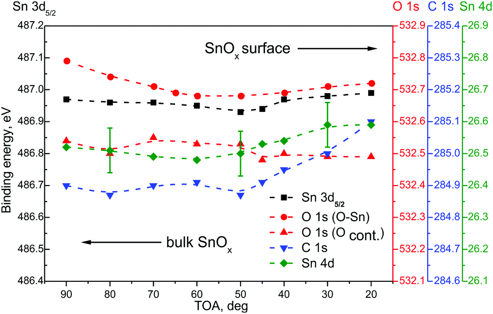 | ||
| Fig. 3 Core level energy recorded with ADXPS for Sn 3d5/2 (black), O 1s (red), C 1s (blue) and Sn 4d (green) energy regions in RGVO–SnOx. The error bars were marked only for one component to keep the image clear. | ||
A detectable variation was only found for the C 1s component at the vicinity of the RGVO–SnOx surface. It points to the existence of a surface dipole-like or charging-like effect caused by the contaminating organic adsorbates. Consequently, the carbonaceous adsorbate layer is “passivating” electrically the RGVO–SnOx surface, preventing the oxide-related core levels from interacting noticeably with the outer space.
After CuPc layer deposition, the situation of the energy shifts of RGVO–SnOx related core levels is not altered in its majority as shown in Fig. 4. The bottom part of Fig. 4 presents the RGVO–SnOx-related energy shift of core levels Sn 3d5/2, O 1s and Sn 4d. The upper part of the figure shows the core level shift of the CuPc-related components.
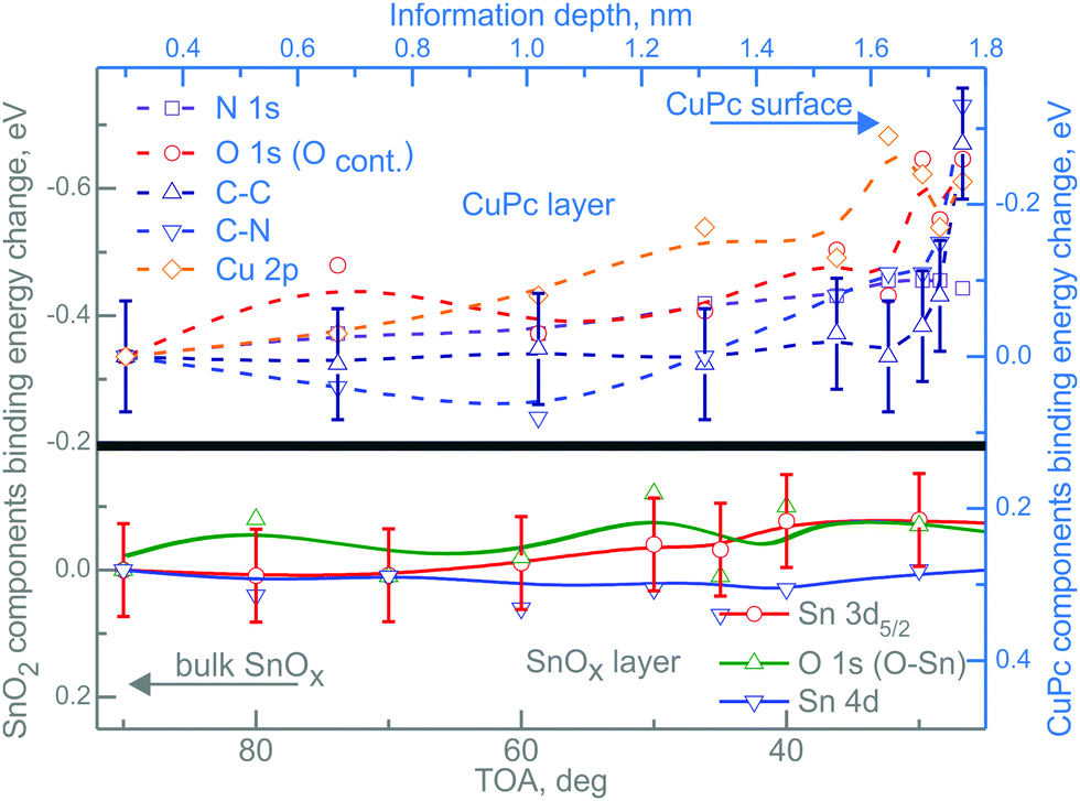 | ||
Fig. 4 Depth-dependent core level energy shifts for RGVO–SnOx/CuPc. The bottom-left, gray ( ) scale corresponds to the RGVO–SnOx layer (solid lines), while the top-right blue scale ( ) scale corresponds to the RGVO–SnOx layer (solid lines), while the top-right blue scale ( ) stands for the CuPc layer. All of the lines have been fitted to polynomials to guide the eye. Error bars were marked only for one exemplary component for each layer, and are of the same order of magnitude throughout the dataset. Note that the information depth used here is not the same as the relative depth used in the RDP analysis in Fig. 2. ) stands for the CuPc layer. All of the lines have been fitted to polynomials to guide the eye. Error bars were marked only for one exemplary component for each layer, and are of the same order of magnitude throughout the dataset. Note that the information depth used here is not the same as the relative depth used in the RDP analysis in Fig. 2. | ||
Due to the fact that the depth calculations for the ADXPS method are done with respect to the sample surface, all calculations, such as IMFP and attenuation length, were performed with CuPc-related material constants. Consequently, the respective energy changes in the oxide layer had to be plotted as function of TOA. Practically, the higher the TOA, the greater the depth out of which the majority of the signal is coming from.
While there is no detectable depth dependence of the core levels of RGVO–SnOx, the situation is more complicated for the CuPc-related core levels N 1s, O 1s including adsorbed contamination Ocont, C–N, C–C and Cu 2p. The most interesting in the scope of this study is the core level shift in the proximity of the interface. Analyzing the component energy positions as a function of information depth, one finds no significant shift within the first ∼1.5 nm from the RGVO–SnOx/CuPc interface. On the other hand, all of the components except the N 1s region, experience a shift of ∼0.2 eV in the vicinity of the CuPc surface. Since the N 1s region is not being shifted, charging-induced effects can safely be neglected.
The experimental observations raise the question of the reason for the lack of mobile charge transfer via the RGVO–SnOx/CuPc interface, causing the continuous shift of the energy levels at both sides of the junction. Next, we haven’t got any detectable photoemission evidence for mobile charge transfer via the interface, so we can exclude or at least ignore eventual discontinuances of contaminants’ cover.
The most likely interpretation led us to the conclusion that the energy levels from both sides of the interface are not fully aligned. One of the reasons for the missing alignment could be that a charge transfer via the RGVO–SnOx/CuPc interface is being blocked by a passivating layer of adsorbed adventitious carbon. Small organic compounds are present especially in indoor atmospheres e.g. in the form of volatile organic compounds (VOCs). Compounds present include e.g. low molecular weight carboxylic acids such as acetic acid or lactic acid as products from oxidation of paper or wood.63 The whole group of possible organic compounds in a general indoor atmosphere is diverse.64 Some of the organic compounds adsorb, possibly under chemical reaction, on the freshly prepared surfaces during exposure to ambient lab atmosphere. The resulting effect on the electronic structure looks similar to energy level pinning at the interface which was described in various systems.65,66 However this effect is commonly attributed to the existence of a significant number of metal-induced intra-gap states,67 a polaron level in the organic material,68 or to the case when the organic's ionization energy equals the substrate's Fermi level.69 Here, we do not find any of these cases. Consequently, the most probable explanation is that the lack of mobile charge transfer is caused by organic adsorbates at the interface. As hydrocarbons have a large gap between the highest occupied molecular orbital (HOMO) and the lowest unoccupied molecular orbital (LUMO), they are expected to act as molecular insulators.70 Although the presented results appear as surprising at first sight, such an effect was observed in the literature earlier for similar systems.3,71
In order to support the conclusion that carbonaceous adsorbates can be blocking charge transfer via the inorganic/organic interface, semi-empirical calculations were done for two minimalistic model systems, (i) a tin oxide cluster in contact with a CuPc molecule and (ii) a system with organic adsorbates between an oxide cluster and CuPc [Fig. 5(a)]. Clusters are used for modeling the oxide's surfaces mainly in the study of localized structures and phenomena where the periodic approach can be computationally aggravating. Examples of such objects are foreign impurities that induce local charge distributions.49,51 Since these simulations are focused on the influence of organic adsorbates on the charge transfer, required results can be obtained using clusters with a good approximation without high complexity of the calculations. To model a SnO2 surface covered with organic adsorbates, CH3 groups were placed bound to the oxygen atoms, mimicking organic adsorbates changing the original Sn3O4(OH)4 cluster to Sn3O4(CH3)4 [Fig. 5(b)]. Hence a full geometry optimization and partial charge computation was performed for the following structures: Sn3O4(OH)4 [Fig. 5(a)], Sn3O4(OCH3)4 [Fig. 5(b)], the CuPc molecule, [Fig. 5(c)], Sn3O4(OH)4 with CuPc [Fig. 5(d)], and Sn3O4(OCH3)4 with CuPc [Fig. 5(e)].
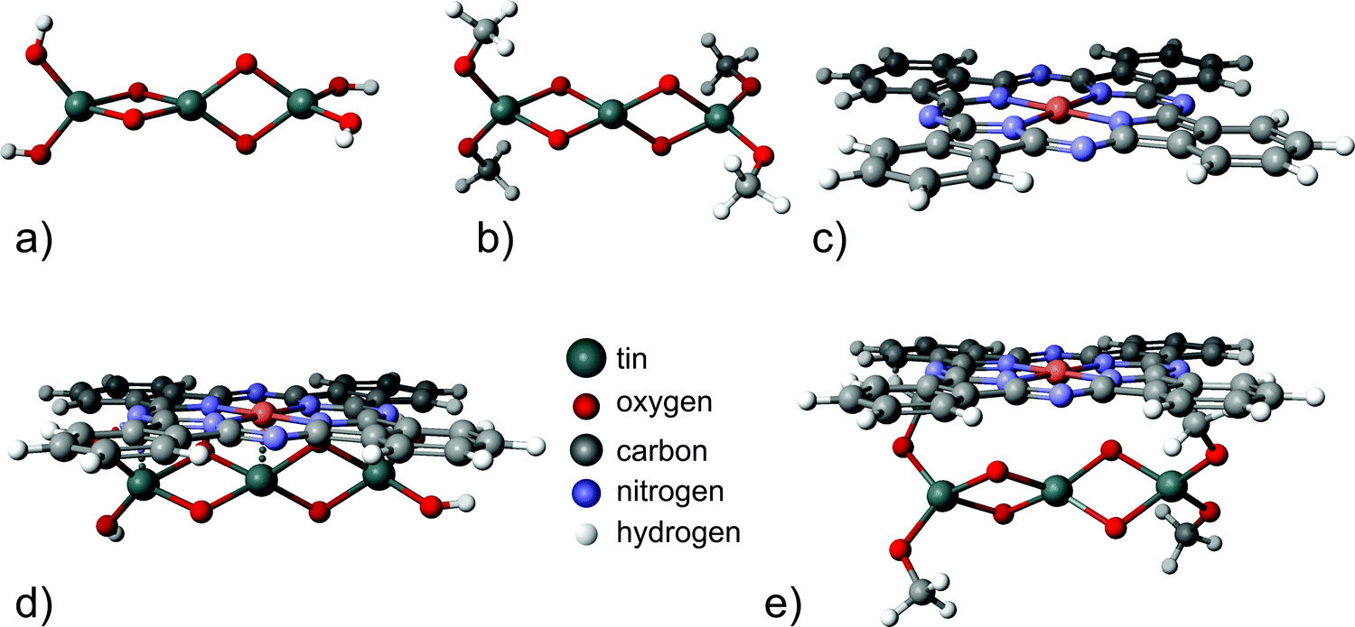 | ||
| Fig. 5 Structures used for modeling: (a) the Sn3O4(OH)4 cluster, (b) the Sn3O4(CH3)4 cluster, (c) the CuPc molecule, (d) Sn3O4(OH)4 with CuPc and (e) Sn3O4(CH3)4 with CuPc. | ||
In the next step, partial charges for all optimized configurations were determined. To quantify the charge transfer between SnO2 and CuPc, the total value of the electrical charge on the Sn3O4(OH)4 cluster and CuPc molecule was calculated for both variants: isolated molecules and Sn3O4(OH)4 with CuPc. The same analysis was carried out for Sn3O4(OCH3)4 and CuPc. The results are presented in Table 1. It can be observed that for the structure without organic adsorbates, a charge transfer of about 0.327 e occurs, while for the one with organic adsorbates it is about 0.039 e lower. The geometries of bare tin dioxide with CuPc and carbon-contaminated oxide with CuPc are presented in Fig. 5(d and e) respectively. Although the change in the amount of the charge transferred across the interface is low, the simulated system presents a minimalistic model only. From the obtained geometries, it is obvious that placing the “insulating” methyl groups on the tin oxide surface lead to a larger spatial separation between the tin oxide surface and CuPc. As electronic interactions decay exponentially with distance,72 the larger distance between the solid oxide and CuPc in the presence of aliphatic organic adsorbates leads to a lower overlap of molecular orbitals, and hence lowers the charge transfer. This lowering of charge transfer is expected as long as the adsorbate has a large HOMO–LUMO gap, as in the case of aliphatic chains. In reality, the spatial separation between tin oxide and CuPc is likely larger, because longer chains may be involved in the adsorption. The likely presence of longer chains is based on the shape of the C 1s peak, which is not consistent with a large fraction of oxygen bound carbon of carboxylic acids.63 With a methyl group as the minimalistic, smallest possible model, all more realistic descriptions must involve a longer separating distance between SnO and CuPc than explored in the model, consequently, dampening molecular interactions even to a larger extent.
| Structure | Total charge [e] | |
|---|---|---|
| Sn3O4(OH)4 | 0 | |
| Sn3O4(OCH3)4 | −0.002 | |
| CuPc | −0.005 | |
| Sn3O4(OH)4 + CuPc | Sn3O4(OH)4 | CuPc |
| 0.325 | −0.327 | |
| Sn3O4(OCH3)4 + CuPc | Sn3O4(OCH3)4 | CuPc |
| 0.287 | −0.288 | |
However, the quantities obtained from the simulations should not be overinterpreted, since the MO–G module treats valence electrons only. Hence changes in inner shell electron properties may have been ommitted. Rather, they are a supporting argument but not the ultimate proof, since the simulation was performed on a significantly simplified model of the examined system. Nevertheless the tendency of the obtained results agrees well with the experimental data.
To obtain a more comprehensive description of the examined layers’ electronic properties, UPS measurements were done in the He I excitation range. The He I line was chosen due to the fact that with an average information depth of 2 nm it gives us more “bulk” information in comparison to the He II line which is purely surfacial.73Fig. 6 presents parts of the UPS spectrum obtained for both types of examined samples. Fig. 6(a) shows the magnified valance band region recorded for bare RGVO–SnOx layers. Following procedures proposed by Ishii et al.,74 the top of the valance band EV was fitted with a straight line to the square root of intensity, which is recommended in the case of metals and metal oxide samples. The increasing signal between EF and EV can be assigned largely to defect level contributions resulting mainly from Sn 5p/5s orbitals. In addition, the deviation from a linear increase of the background also contributes. Fig. 6(b) presents the HOMO peak energy region for RGVO–SnOx/CuPc layers. Although the HOMO peak is not very intense, the onset of the HOMO peak EHOMO can be determined.
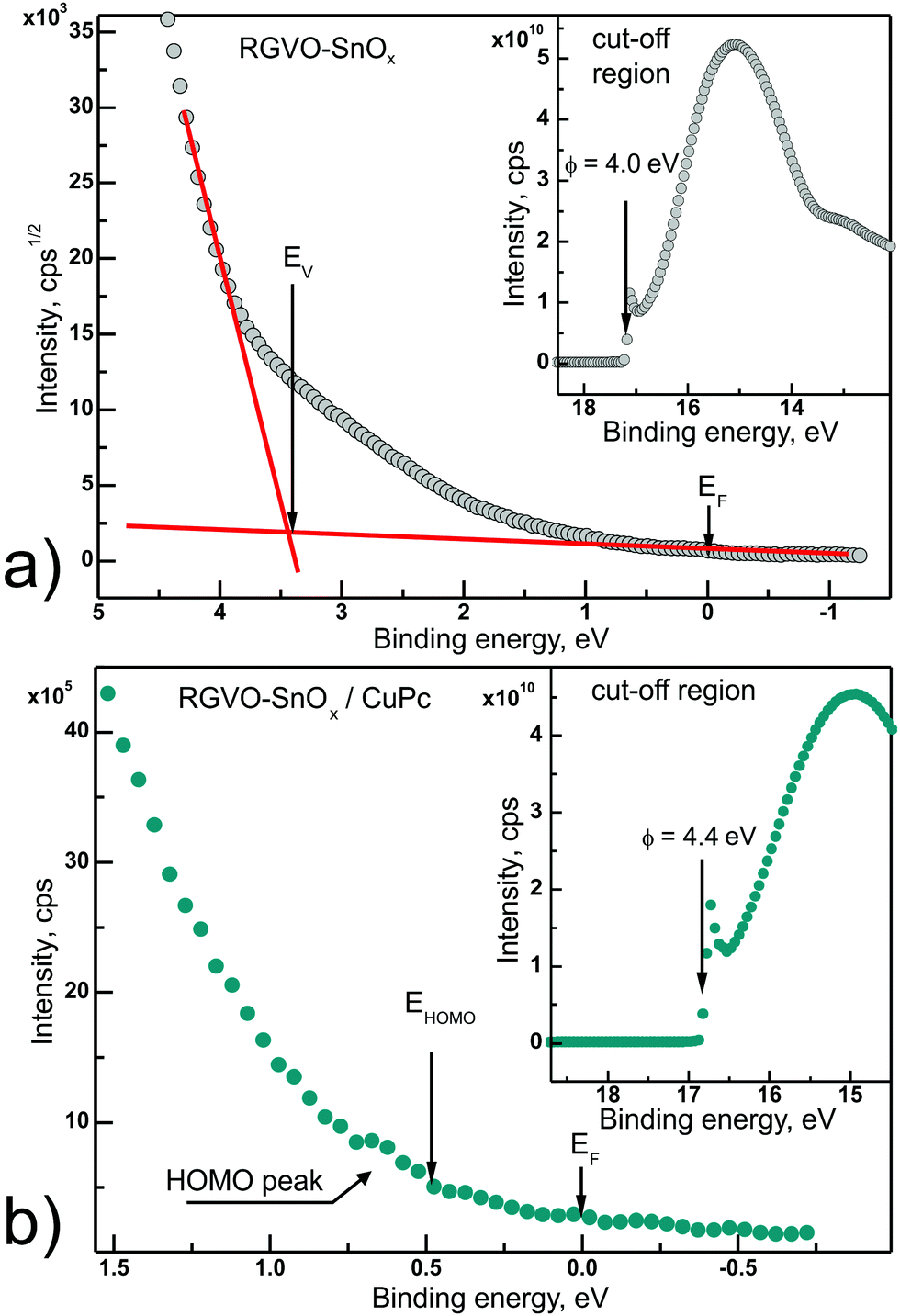 | ||
| Fig. 6 UPS results obtained for bare RGVO–SnOx layers (a) and RGVO–SnOx/CuPc (b). The main panels present the valance band (RGVO–SnOx) and HOMO (RGVO–SnOx/CuPc) energy regions. Zero binding energy is assigned to the position of the Fermi level EF. The insets to the figures present the high-energy cut-off, allowing determination of the samples’ work function ϕ. | ||
The insets to both Fig. 6 panels show high-binding energy cut-offs Ecut-off allowing determination of the samples’ work function ϕ following the dependence75ϕ = Eexc − Ecut-off, where Eexc is the excitation energy, here 21.22 eV. As a result, for bare RGVO–SnOx layers the determined ϕ = (4.00 ± 0.05) eV and for CuPc-covered oxide ϕ = (4.40 ± 0.05) eV. While for the RGVO–SnOx/CuPc layers the value of ϕ is quite consistent with the literature data for CuPc ultra-thin layers,76 the 4.0 eV obtained for bare oxide is lower than for similar systems.77 This result is consistent with the increased electron concentration revealed by XPS in the adventitious carbon layer, which is manifested as a ∼0.2 eV shift of the C 1s level towards higher binding energy, with a lack of a similar simultaneous trend in the rest of the oxide-related core levels. This increased electron concentration induces a reduction of the RGVO–SnOx work function as detected by UPS. The magnitude of the ∼0.4 eV shift in the work function at the interface revealed by UPS will be discussed further below.
The performed UPS experiment allowed also determination of the ionization energies IE, i.e. the energy distance from the vacuum level EVAC to EV for RGVO–SnOx, or EHOMO for CuPc. Following the relation IE = ϕ + (EF − EV),74IE = 7.4 eV and 4.9 eV for the bare oxide and the CuPc-covered oxide, respectively. Both values are in reasonable agreement with available literature values.27,28
Merging the photoemission results obtained by different excitation techniques, it is possible to construct a band-like energy level positioning diagram presenting in a simplified form the energy structure of the RGVO–SnOx/CuPc system as presented in Fig. 7(a). The energy level changes plotted in the diagram are as detected for the RGVO–SnOx/CuPc structure with the exception of region (II). This region is showing the situation of the bare oxide surface, i.e. is showing the shift of the contamination-related C–C component with no shift of the others. The only reaction of the energy levels is the shift of the C 1s region. Region (III) corresponds to the CuPc layer in the vicinity of the RGVO–SnOx/CuPc interface, lacking a detectable energy level shift as well. Together with the absence of a detectable shift of the RGVO–SnOx-related core levels and with the significant interface dipole effect detected by UPS, one can conclude that the energy levels are not fully aligned. The interface dipole is compensating for the difference of the Fermi levels from both sides of the interfacial region (II), however, the particular levels are not being shifted. Hence a mobile charge transfer via the interface which should allow charge equalization did not occur. We used the term “interface dipole” between inorganic/organic layers after Hill et al.78 who indicated the dipole effect as the result of polarization of the first organic molecular layer at the interface. Here we deal with the narrow rearrangement of localized electronic charge which is mirrored by the abrupt shift of potential at the interface.56,79
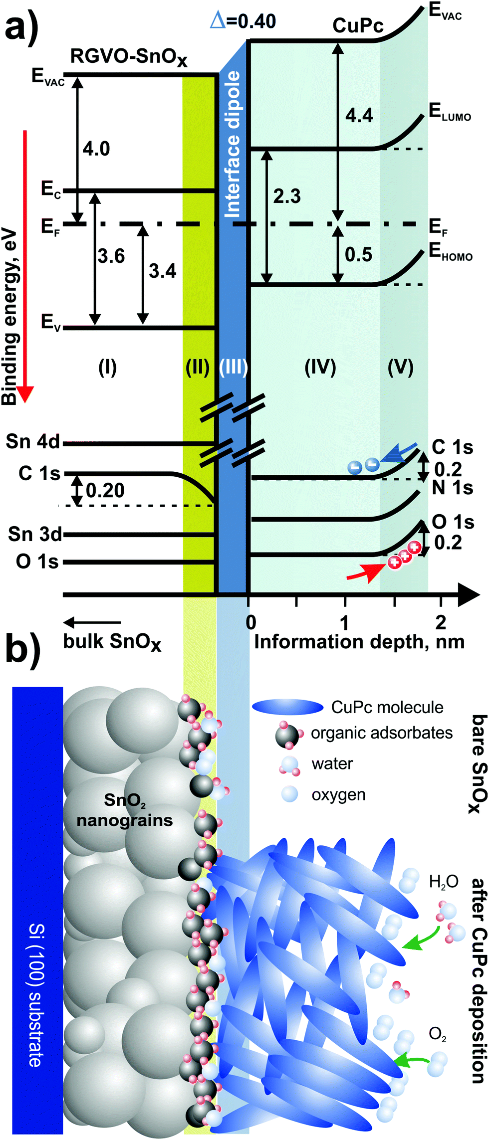 | ||
| Fig. 7 Energy level diagram (a) presenting energy level positioning derived from photoemission methods. Roman numbers in brackets correspond to: (I) – the subsurface of RGVO–SnOx; (II) – the region with surface–environment interaction of bare RGVO–SnOx; (III) – the RGVO–SnOx/CuPc interface; (IV) – the CuPc layer; (V) – the region with CuPc–environment interaction. All of the values are given in eV. Part (b) presents a cartoon showing a model of the examined system. The upper part of the cartoon corresponds to the situation of the bare RGVO–SnOx layer. The bottom part represents the same layer after CuPc deposition. The intermediate organic adsorbate contamination layer is preventing the charge transfer via the inorganic/organic interface. The surface shifts of the energy levels detected are caused by adsorbed molecules generating a surface dipole or band bending-like effect. | ||
The last region (IV) is showing the CuPc surface–environment interaction after the deposition process. The effect of majority carrier accumulation due to oxidizing species adsorption leads to an upward shift of the energy levels. The effect is consistent with previous studies on surface–environment interactions of CuPc layers.55 The magnitude of the detected surface effect is at ∼0.2 eV sufficiently small, so its impact on the deeper part of the CuPc layer remains negligible.
The diagram is followed by the cartoon-style summary [Fig. 7(b)] of the examined system, which highlights the major phenomena taking place at the surfaces of oxide and CuPc. The shaded areas are eye-guiding for an easy correlation between Fig. 7(a and b).
An implication of the results from this work is that although vacuum deposition techniques provide clean surfaces during in situ processing, these surfaces are highly reactive. Thus, they are rapidly saturated with adsorbates when exposed to an ambient environment. As expected, such adsorption could be a significant problem for manufacturing of multilayered electronic devices, due to the probability of charge transport blocking at the contaminated interface. Comparing these results to previously mentioned non-UHV sol–gel techniques, it is obvious that either it is better to prepare the oxide films with uniformly distributed adsorbates, or one has to plan surface cleaning processes before each production step. The latter is time-consuming and costly, and additionally complicates the whole process. In addition, cleaning processes like plasma or ion etching can cause further damage to the samples surfaces. While such problems can be circumvented by using UHV-only methods, these offer a limited chemical versatility and make the whole process costly.
On the other hand, the carbonaceous layer between RGVO–SnOx and CuPc was passivating the oxide film, making it immune to further changes in electronic structure. This effect could be applied for cost-effective transportation of the oxide films between different vacuum-based processing stages. If the surface structure is not volatile during cleaning processes, UHV annealing accompanied by e.g. low energy ion etching could be used to restore the charge transport capability of the interface.
Summary and conclusion
An RGVO–SnOx/CuPc buried interface was investigated by depth- and energy resolved photoemission spectroscopy methods. The central point was the revelation of the impact from adsorbates at the SnOx/CuPc interface on the energy level alignment between the oxide layer and the organic ultra-thin film.The adsorbates, which are mainly what is commonly referred to as adventitious carbon, are located at the surface of the examined oxide structure, not mixed within subsurface and bulk areas. There is no detectable energy shift in the vicinity of the bare RGVO-–SnOx surface, as shown by analysis of the core levels. The only detectable shift was related to the carbon adsorbate layer signal. Consequently, the organic adsorbates are blocking electronic interactions between the environment and the surface, pinning the energy levels.
After the CuPc film deposition, the investigations revealed no substantial variation of the core level energy position in the proximity of the RGVO–SnOx/CuPc interface from both sides. By application of UPS, a significant interface dipole of 0.4 eV was detected. It was concluded that the dipole is compensating for the difference in work functions of the materials in contact, however, energy levels are not fully aligned as a consequence. A shift of ∼0.2 eV of CuPc-related core levels in the vicinity of the film surface is related to CuPc–environment interactions after the deposition process.
A consequence of the results from this study is that environment related adsorbates on oxide surfaces could be utilized for passivation-like processes, although not as controlled as traditional techniques. However, if it is required to keep the oxide surface interactions fully accessible, like e.g. in the case of stacked electronic systems or gas sensor applications, organic adsorbates must be carefully avoided in each processing step. Allowing parasitic adsorption to occur would lead to a lack of energy level alignment and hence charge transfer. Therefore, in situ structure preparation is crucial if there are any obstacles for sample cleaning, like by ion etching or annealing.
Conflicts of interest
There are no conflicts to declare.Acknowledgements
This work was partially supported by the Polish budget for science in years 2013–2015 by the Ministry for Science and Higher Education within Iuventus Plus IP2012 019072 project through the Silesian University of Technology, Institute of Physics. Authors acknowledge the ESPEFUM laboratory at the Institute of Physics – CSE, Silesian University of Technology for access to the UPS experimental setup. Special thanks go to prof. Jerzy Bodzenta and prof. Andrzej Bluszcz for continuous support. Open Access funding provided by the Max Planck Society.References
- A. Balandin, Nat. Mater., 2011, 10, 569 CrossRef PubMed.
- N. Chen, C. Huang, W. Yang, S. Chen, H. Liu, Y. Li and Y. Li, J. Phys. Chem. C, 2010, 114, 12982 Search PubMed.
- Characterization of Semiconductor Heterostructures and Nanostructures, ed. C. Lamberti and G. Agostini, Elsevier, Amsterdam, 2013 Search PubMed.
- S. K. Saha, A. Guchhait and A. J. Pal, Phys. Chem. Chem. Phys., 2014, 16, 4193 RSC.
- S. K. Saha, A. Guchhait and A. J. Pal, Phys. Chem. Chem. Phys., 2012, 14, 8090 RSC.
- J. M. Luther, M. Law, M. C. Beard, Q. Song, M. O. Reese, R. J. Ellingson and A. J. Nozik, Nano Lett., 2008, 8, 3488 CrossRef PubMed.
- A. Guchhait and A. J. Pal, J. Phys. Chem. C, 2010, 114, 19294 Search PubMed.
- J. Androulakis, C. Lin, H. Kong, C. Uher, C. Wu, T. Hogan, B. Cook, T. Caillat, K. Paraskevopoulos and M. Kanatzidis, J. Am. Chem. Soc., 2007, 129, 9780 CrossRef PubMed.
- L. Wang, M.-H. Yoon, G. Lu, Y. Yang, A. Facchetti and T. J. Marks, Nat. Mater., 2006, 5, 893 CrossRef PubMed.
- T. B. Fleetham, J. P. Mudrick, W. Cao, K. Klimes, J. Xue and J. Li, ACS Appl. Mater. Interfaces, 2014, 6, 7254 Search PubMed.
- T. Fleetham, B. O’Brien, J. P. Mudrick, J. Xue and J. Li, External. Appl. Phys. Lett., 2013, 103, 083303 CrossRef.
- G. Bersuker, C. S. Park, J. Barnett, P. S. Lysaght, P. D. Kirsch, C. D. Young, R. Choi, B. H. Lee, B. Foran, K. van Benthem, S. J. Pennycook, P. M. Lenahan and J. T. Ryan, Appl. Phys. Lett., 2006, 100, 094108 Search PubMed.
- G. Li, R. Zhu and Y. Yang, Nat. Photonics, 2012, 6, 153–161 CrossRef.
- W. Li, A. Furlan, K. H. Hendriks, M. M. Wienk and R. A. Janssen, J. Am. Chem. Soc., 2013, 135, 5529–5532 CrossRef PubMed.
- L. Mercier and T. J. Pinnavaia, Chem. Mater., 2000, 12, 188 CrossRef.
- M. A. Pietrzyk, M. Stachowicz, P. Dluzewski, A. Wierzbicka and A. Kozanecki, J. Alloys Compd., 2018, 737, 748 CrossRef.
- S. H. Park, H. J. Kim, M.-H. Cho, Y. Yi, S. W. Cho, J. Yang and H. Kim, Appl. Phys. Lett., 2011, 98, 082111 CrossRef.
- Y. R. Ryu, T. S. Lee and H. W. White, J. Cryst. Growth, 2004, 261, 502 CrossRef.
- A. S. Komolov, S. A. Komolov, E. F. Lazneva, A. A. Gavrikov and A. M. Turiev, Surf. Sci., 2011, 605, 1452 CrossRef.
- S. Sinha and M. Mukherjee, J. Appl. Phys., 2013, 114, 083709 CrossRef.
- N. Tsuda, Electronic Conduction in Oxides, Springer Science & Business Media, 2000 Search PubMed.
- Y. S. Zhang, D. X. Wang, Z. Y. Wang and Y. Y. Wang, Opt. Quantum Electron., 2016, 48, 18 CrossRef.
- O. A. Melville, B. H. Lessard and T. P. Bender, ACS Appl. Mater. Interfaces, 2015, 7, 13105 Search PubMed.
- Ch. D. Dimitrakopoulos and P. R. L. Malenfant, Adv. Mater., 2002, 14, 99 CrossRef.
- P.-L. Ong and I. A. Levitsky, Energies, 2010, 3, 313 CrossRef.
- Z. Hachoun, A. Ouerdane, M. Bouslama, M. Ghaffour, A. Abdellaoui, Y. Caudano and A. Ali benamara, IOP Conf. Ser.: Mater. Sci. Eng., 2016, 123, 012029 CrossRef.
- M. Batzill, K. Katsiev and U. Diebold, Appl. Phys. Lett., 2004, 85, 5766 CrossRef.
- M. Krzywiecki and L. Grządziel, Appl. Surf. Sci., 2014, 311, 740 CrossRef.
- J. G. Van Dijken and M. J. Brett, Molecules, 2012, 17, 10119 CrossRef PubMed.
- Y. Gao, Mater. Sci. Eng. Carbon, 2010, 68, 39 CrossRef.
- F. de Groot and A. Kotani, Core Level Spectroscopy of Solids, CRC Press, Taylor & Francis Group, Boca Raton, 2008 Search PubMed.
- M. Krzywiecki, A. Sarfraz and A. Erbe, Appl. Phys. Lett., 2015, 107, 231601 CrossRef.
- M. Kwoka and M. Krzywiecki, Beilstein J. Nanotechnol., 2017, 8, 514 CrossRef PubMed.
- http://www.casaxps.com .
- I. Lindau, P. Pianetta, K. Y. Yu and W. E. Spicer, Phys. Rev. B: Solid State, 1976, 16, 492 CrossRef.
- R. L. Opila and J. Eng Jr., Prog. Surf. Sci., 2002, 69, 125 CrossRef.
- http://www.thermoscientific.com/en/product/theta-probe-angle-resolved-x-ray-photoelectron-spectrometer-arxps-system.html .
- P. Seah and W. A. Dench, Surf. Interface Anal., 1979, 1, 2 CrossRef.
- C. J. Powell and A. Jablonski, NIST Electron Inelastic-Mean-Free-Path Database, Version 1.2, SRD 71, National Institute of Standards and Technology, Gaithersburg, MD, 2010 Search PubMed.
- W. S. M. Werner, Surf. Interface Anal., 1992, 18, 217 CrossRef.
- S. Tanuma, C. J. Powell and D. R. Penn, Surf. Interface Anal., 1993, 21, 165 CrossRef.
- P. J. Cumpson, Surf. Interface Anal., 2000, 29, 403 CrossRef.
- R. Pilolli, N. Ditaranto, N. Cioffi and L. Sabbatini, Anal. Bioanal. Chem., 2013, 405, 713 CrossRef PubMed.
- C. R. Brundle, G. Conti and P. Mack, J. Electron Spectrosc. Relat. Phenom., 2010, 178–179, 433 CrossRef.
- M. Arndt, J. Duchoslav, H. Itani, G. Hesser, C. K. Riener, G. Angeli, K. Preis, D. Stifter and K. Hingerl, Anal. Bioanal. Chem., 2012, 403, 651 CrossRef PubMed.
- J. R. Taylor, An Introduction to Error Analysis: The Study of Uncertainties in Physical Measurements University Science Books, Sausalito, 1997 Search PubMed.
- D. Ehre and H. Cohen, Appl. Phys. Lett., 2013, 103, 052901 CrossRef.
- A. Givon and H. Cohen, Surf. Interface Anal., 2015, 47, 607 CrossRef.
- T. S. Rantala, V. Lantto and T. T. Rantala, Phys. Scr., 1994, T54, 252–255 CrossRef.
- T. S. Rantala, V. Golovanov and V. Lantto, Sens. Actuators, B, 1995, 24-25, 532–536 CrossRef.
- M. Melle-Franco and G. Pacchioni, Surf. Sci., 2000, 461, 54–66 CrossRef.
- A. Robina, E. Germán, M. E. Pronsato, A. Juan, I. Matolínová and V. Matolín, Vacuum, 2014, 106, 86 CrossRef.
- http://www.fqs.pl/en/chemistry/products/scigress .
- D. A. Evans, H. J. Steiner, S. Evans, R. Middleton, T. S. Jones, S. Park, T. U. Kampen, D. R. T. Zahn, G. Cabailh and I. T. McGovern, J. Phys.: Condens. Matter, 2003, 15, S2729 CrossRef.
- L. Grządziel and M. Krzywiecki, Synth. Met., 2015, 210 B, 141 CrossRef.
- H. Peisert, M. Knupfer, T. Schwieger, J. M. Auerhammer, M. S. Golden and J. Fink, J. Appl. Phys., 2002, 91, 4872 CrossRef.
- L. Grządziel, M. Krzywiecki, G. Genchev and A. Erbe, Synth. Met., 2017, 223, 199 CrossRef.
- http://www.lasurface.com .
- M. Krzywiecki, L. Grządziel, A. Sarfraz and A. Erbe, Phys. Chem. Chem. Phys., 2017, 19, 11816 RSC.
- A. F. Hollemann and E. Wiberg, Lehrbuch der Anorganischen Chemie, de Gruyter, Berlin, 101st edn, 1995 Search PubMed.
- A. S. Komolov, S. N. Akhremtchik and E. F. Lazneva, Spectrochim. Acta, Part A, 2011, 79, 708 CrossRef PubMed.
- L. Grzadziel, M. Krzywiecki, H. Peisert, T. Chassé and J. Szuber, Thin Solid Films, 2011, 519, 2187 CrossRef.
- M. Jablonsky, K. Hrobonova, S. Katuscak, J. Lehotay and M. Botkova, Cellul. Chem. Technol., 2012, 46, 331–340 Search PubMed.
- B. Zabiegała, Pol. J. Environ. Stud., 2006, 15, 383 Search PubMed.
- A. C. Graham, D. L. Sawkey, M. Pepper, M. Y. Simmons and D. A. Ritchie, Phys. Rev. B: Condens. Matter Mater. Phys., 2007, 75, 035331 CrossRef.
- H. Vázquez, W. Gao, F. Flores and A. Kahn, Phys. Rev. B: Condens. Matter Mater. Phys., 2005, 71, 041306(R) CrossRef.
- A. Dimoulas, P. Tsipas, A. Sotiropoulos and E. K. Evangelou, Appl. Phys. Lett., 2006, 89, 252110 CrossRef.
- C. Tengstedt, W. Osikowicz, W. R. Salaneck, I. D. Parker, C.-H. Hsu and M. Fahlman, Appl. Phys. Lett., 2006, 88, 053502 CrossRef.
- M. T. Greiner, M. G. Helander, W.-M. Tang, Z.-B. Wang, J. Qiu and Z.-H. Lu, Nat. Mater., 2012, 11, 76 CrossRef PubMed.
- C. Boulas, J. V. Davidovits, F. Rondelez and D. Vuillaume, Phys. Rev. Lett., 1996, 76, 4797 CrossRef PubMed.
- M. Glaser, H. Peisert, H. Adler, M. Polek, J. Uihlein, P. Nagel, M. Merz, S. Schuppler and T. Chasse, J. Phys. Chem. C, 2015, 119, 27569 Search PubMed.
- P. Atkins and J. de Paula, Atkins’ Physical Chemistry, Oxford University Press, Oxford, 2010 Search PubMed.
- P. Seah and W. A. Dench, Surf. Interface Anal., 1979, 1, 2 CrossRef.
- Electronic Processes in Organic Electronics, ed. H. Ishii, K. Kudo, T. Nakayama and N. Ueno, Springer, Tokyo, 2015 Search PubMed.
- P. Y. Yu and M. Cardona, Fundamentals of Semiconductors-Physics and Materials Properties, Springer-Verlag, Berlin, Heidelberg, 2001 Search PubMed.
- A. S. Komolov, E. F. Lazneva, S. A. Komolov, P. S. Repin and A. A. Gavrikov, Semiconductors, 2012, 46, 988 CrossRef.
- T. J. Whitcher, K. H. Yeoh, C. L. Chua, K. L. Woon, N. Chanlek, H. Nakajima, T. Saisopa and P. Songsiriritthigul, Curr. Appl. Phys., 2014, 14, 472 CrossRef.
- I. G. Hill, J. Schwartz and A. Kahn, Org. Electron., 2000, 1, 5 CrossRef.
- H. Ishii, K. Sugiyama, E. Ito and K. Seki, Adv. Mater., 1999, 11, 605 CrossRef.
| This journal is © the Owner Societies 2018 |