
Assessing the scalability of low conductivity substrates for photo-electrodes via modelling of resistive losses
Isaac
Holmes-Gentle
 a,
Harsh
Agarwal
b,
Faye
Alhersh
a and
Klaus
Hellgardt
*a
a,
Harsh
Agarwal
b,
Faye
Alhersh
a and
Klaus
Hellgardt
*a
aDepartment of Chemical Engineering, Imperial College London, London, SW7 2AZ, UK. E-mail: k.hellgardt@imperial.ac.uk
bDepartment of Chemical Engineering, University of Michigan, Ann Arbor, MI 48109, USA
First published on 19th April 2018
Abstract
When scaling up photo-electrochemical processes to larger areas than conventionally studied in the laboratory, substrate performance must be taken into consideration and in this work, a methodology to assess this via an uncomplicated 2 dimensional model is outlined. It highlights that for F-doped SnO2 (FTO), which is ubiquitously used for metal oxide photoanodes, substrate performance becomes significant for moderately sized electrodes (5 cm) under no solar concentration for state of the art Fe2O3 thin films. It is demonstrated that when the process is intensified via solar concentration, current losses become quickly limiting. Methodologies to reduce the impact of substrate ohmic losses are discussed and a new strategy is proposed. Due to the nature of the photo-electrode current–potential relationship, operation at a higher potential where the photo-current saturates (before the dark current is observed) will lead to a minimum in current loss due to substrate performance. Crucially, this work outlines an additional challenge in scaling up photo-electrodes based on low conductivity substrates, and establishes that such challenges are not insurmountable.
1 Introduction
The global energy system is currently reliant on fossil fuels and solar driven photo-electrochemical water splitting is an attractive and sustainable alternative,1–3 although there are currently obstacles to be overcome before commercialisation is realised.4Photo-electrochemical water splitting operates via the photo-excitation of electrons to the conduction band of a semiconductor. The electric field in the semiconductor formed by the semiconductor–electrolyte interface helps separate the newly created electron/hole and a reaction is driven at the surface of the semiconductor. In a photo-anode, holes at the semiconductor–electrolyte junction drive the oxidation of water and electrons are removed from the back of the photo-absorber via a substrate. These excited electrons go on to reduce water at a cathodic site. As shown in Fig. 1, the electrical connection to the counter electrode can either be wired or wireless,5,6 and in this work wired designs will be investigated. In a wired design, the majority carrier, after being transferred from the photo-absorber to the substrate, is collected at the edges of the substrate and an electrical pathway to the opposite electrode is made via an external wire. This is different as compared to the wireless device where the cathode backs directly onto the anode in a monolithic stack.
 | ||
| Fig. 1 Photo-electrochemical device configurations (a) wireless (b) wired. | ||
Currently, notable techno-economic and life cycle analysis have focused on wireless designs which would not suffer from the issue of the size of the electrode (i.e. scale up) being impacted by substrate resistance as charge flows perpendicular to the electrode surface.7,8 However a clear winner in terms of economics has not been established and wired designs have many advantages over wireless designs. Ohmic losses through the solution and current density distributions can be more easily minimised5,9 without the need for perforations of the electrode. A potential bias can be easily applied and this flexibility can be taken advantage of in stacked architectures.10,11
Presently, there exists a trilemma in solar-driven water splitting: simultaneously achieving efficient, inexpensive and stable devices. High conductivity substrates are typically used for III–V type photo-electrodes such as Au.12 Similarly, for mature photo-voltaic technologies coupled with electrolysis, current collection issues have be solved with busbars and highly conductive substrates.13–15 However, there are many examples of devices which use low efficiency and highly stable materials such as metal oxides1,3 which are often deposited on low conductivity substrates.
Transparent Conductive Oxides (TCOs) such as Fluorine-doped Tin Oxide (FTO) are commonly used as substrates for n-type semiconductors in order to form an ohmic junction with the back of the photo-absorber.16,17 Ideally the work function of the substrate should be lower than that of the n-type semiconductor though this heuristic may be further complicated by interface states.18 In the case of α-Fe2O3 on FTO, the work function of the substrate (≈5.0 eV19) is less than the n-type semiconductor (≈5.6 eV20) indicating an ohmic contact is likely formed.
Furthermore, the transparent nature of these substrates may also allow the backside illumination of the photo-electrode. The effect of illumination direction on quantum efficiency was first investigated by Lindquist et al.21 and for films such as BiVO4, which have a low electron mobility compared to hole mobility, back-side illumination may improve quantum yields.22
For the reasons previously outlined, there are many implementations of FTO used as a substrate for Fe2O3,23–25 BiVO4,22 TiO226,27 and WO3 thin films.28,29 Whilst there are examples of non TCO based substrates such as Fe2O3 on titanium30 and nano-structured metal oxides grown from pure metal sheets,31,32 TCO substrates are sufficiently ubiquitous in the solar water splitting field (cf. a recent paper in EES33) as to require further study into the issues involved with current collection over large areas. Current research is often confined to small electrode areas which have yet to reach limiting current densities.16 This will not be the case for scaled up designs where the area of PEC solar collectors will be limited by substrate ohmic losses due to the relatively low conductivities of typical TCOs (cf. copper has a conductivity 100–1000 times higher).
The issue of substrate performance has been studied for thin film solar cells,34–36 but less exhaustively for photo-electrochemical water splitting. The previous modelling work by Carver et al.37 suggested that an area of 5 × 10⁻⁴ m2 (which equates to a square of 2.2 cm side length) will lead to a significant current loss. This work was built on by Farivar38 who came to similar conclusions and suggested implementation of gold back contact in order to circumvent this area restriction. Both models employ a Tafel type current–potential relationship, which being exponential differs significantly from the typical photo-current response.
Fig. 2 shows a typical photo-current vs. potential relationship for a photo-anode. An analytical approximation to the ideal photo-current response can be derived,39,40 but as explained by Memming,41 this commonly deviates from reality for metal oxide semiconductors due to the recombination losses within the depletion layer and at the surface. Another noticeable feature of the photo-oxidation curve is the so called ‘dark current’ observed at high reverse bias, due to the break-down of the junction (similar to the Zener diode breakdown) leading to electron tunnelling through the thin depletion layer.42
 | ||
| Fig. 2 Approximate shape of photo-current curve. | ||
The real photo-current response is represented poorly by a Tafel equation as it has a plateau where a reduction in potential results in a relatively small reduction in current. Hence a more advanced analysis than previously conducted is required in order to understand the effect of substrate performance on the behaviour of the photo-electrode.
Mathematical modelling has the ability to focus and direct solar fuel research. An example of this is the design implications for PECs outlined by Döscher et al.43 when the absorption of solar spectrum in the electrolyte is taken into consideration. In this work, we assess one aspect which limits the scalability of TCOs, so as to act as a clearly defined problem statement to catalyse further research.
2 Theory
In order to analyse the impact of scaling up PECs based on TCO substrates, a model was set up comprising of the relevant physics, assumptions and boundary conditions. The geometry of the PEC cell considered from henceforth is a square of side length L where electrical contact is made to two opposite sides.Ohm's law (1) and the continuity of charge (2) is used in order to simulate the electric currents through a conductive medium under an electric field. Here, J is the current density vector, σ the conductivity (= 1/ρ), E the electric field and Φ the electric potential. The term Q is the current sources/sinks within the medium.
| J = σE | (1) |
| ∇·J = Q | (2) |
| E = −∇Φ | (3) |
The boundaries are modelled as a fixed potential or by specifying the current density. Ohmic contact to the semiconductor is modelled as a Dirichlet boundary condition, Φ = Φ0, where the potential is fixed at some absolute potential (which can be related to an electrode potential U0). Insulating boundaries are created by setting n·J = 0 where n is the normal vector to the surface/boundary. In the region where the electrochemical reaction occurs, the current flows as some function of electrode potential J = f(U) where electrode potential is given by U = Φ − Φelectrolyte + constant. Here Φ is potential of the substrate, Φelectrolyte the potential of the electrolyte and the constant is related to the arbitrary reference electrode system used. In the case of a Butler–Volmer relationship this can be analytically written as eqn (4).
| JBV = J0(eβa(U−Ueq) − e−βc(U−Ueq)) | (4) |
There are various analytical approximations for the photo-current response such as those derived by Gärtner39 and Reichman.40 Built on work by Peter,44,45 a recent paper by Hankin et al.,46 multiplied an empirically derived non-ideality factor with the ‘Gärtner’ equation to give an analytical equation which better approximated experimental data. Non-ideality is approximated by a logistic function which captures the recombination effects. Numerical solution of the charge transport equations may also lead to accurate modelling of photo-current response.47–49
However, these methods of modelling are complex and require accurate knowledge of material parameters, so a more simplistic approach was taken here similar to the methodology used in our previous work.10 In this work it is assumed that the intrinsic photo-current vs. electrode potential relationship could be measured using a sufficiently small sample size such that the issue of current density distributions across the substrate is negligible and these experimentally measured values were taken to approximate the intrinsic current density. If this assumption is inaccurate and the current density recorded is reduced due to substrate performance, then the conclusions in the following analyses constitute a best case scenario and hence reinforces the ramification that substrate performance must be considered when scaling up.
For the purposes of providing the model with a continuous and smooth representation of the discrete data points taken for the intrinsic current density J, a fitted model was used comprising of the summation of the photocurrent Jphoto and the dark current Jdark (eqn (5)). These are represented by a 5-point logistic equation and a Tafel equation respectively (eqn (6) and (7)). As discussed later, in order to approximate higher intensity irradiance, the photocurrent was linearly scaled where S is the number of suns and S0 is the number of suns under which the measurement was performed. This particular form of equation was chosen over alternatives such as a polynomial fit purely for the convenience of obtaining an excellent fit. This fitted equation also facilitated the extrapolation to higher solar intensities which a smooth interpolation method of the data (e.g. splines) would not have provided. A smooth representation of the data is important so as to avoid numerical inaccuracies when calculating ratios at low current densities.
 | (5) |
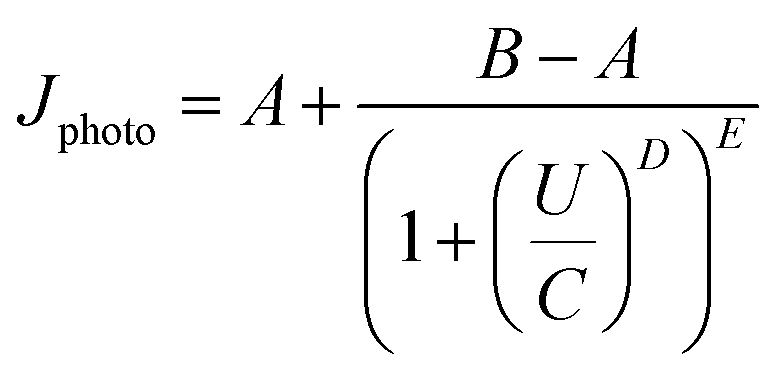 | (6) |
| Jdark = FeG(U−1.23) | (7) |
In order to reduce the computational complexity, the model was reduced from three dimensions to two (i.e. removal of the out of plane dimension z) via the following simplifying assumptions:
• The substrate is sufficiently thin/conductive that there is negligible potential drop in the z direction
• The majority carriers (e− in n-type photo-anode) are transported via the semiconductor normal to the substrate surface prior to transfer to the substrate. This assumption is accurate when the mean diffusion path length for majority carriers in the semiconductor is far smaller than the dimensions of the electrode. This is valid for Fe2O3 (2–4 nm52,53), WO3 (150 nm54) and TiO2 (10 μm55) when compared to an electrode of width of commercially relevant scales
For the 2D model, an out of plane thickness Lz was specified and the photo-current generated is no longer a boundary condition, but re-written as a current source as shown in eqn (8). This formulation of the equations was chosen in order to match the input of the numerical solver.
 | (8) |
Whilst the minimisation of the electrolyte current density distribution is crucial for scale up,37,46,56 the electrolyte current density distribution is neglected in order to isolate the effects of the TCO conductivity on electrode current density. Therefore Φelectrolyte will be a constant at all locations and for simplicity was taken to be zero everywhere.
3 Numerical simulation and parameters
Numerical solution of the partial differential equation was achieved with COMSOL Multiphysics 5.3 and implemented as a stationary electric currents model from the AC/DC module. A full list of parameters used in the simulation can be found in Table 1. A mesh size and solver tolerance sensitivity analysis was conducted to ensure the convergence of the numerical results.Example data for F-doped SnO2 (FTO) was taken as it is currently used more predominately due to it's high temperature stability and reduced cost when compared to In-doped SnO2 (ITO).16 When a substrate out of plane thickness Lz of 300 nm was assumed, the square resistance is approximately 8 Ω sq−1 for the FTO data used (ρ = 2.2 × 10⁻⁶ Ω m), which concurs with the state of the art Pilkington/NSG TEC™ product range.
In order to quantify the intrinsic current density vs. potential relationship of the photo-electrode, example data was taken from literature. Work by Tilley et al.,24 Kim et al.,23 Brillet et al.51 and Kim et al.11 provides cyclic voltammetry (CV) data for exemplary examples of α-Fe2O3, α-Fe2O3, WO3 and BiVO4 deposited on FTO, respectively. Henceforth, these datasets will be referred to as Tilley2010, Kim2013, Brillet2012 and Kim2016. Fitted values to eqn (5)–(7) can be found in Table 2. In this analysis we focus on Tilley2010 due to the larger potential range allowing simulation of system further into dark current producing potentials.
| Parameter | Units | Dataset name | |||
|---|---|---|---|---|---|
| Tilley201024 | Kim201323 | Brillet201251 | Kim201611 | ||
| Material | — | Fe2O3 | Fe2O3 | WO3 | BiVO4 |
| A | A m−2 | 38.7 | 124.3 | 25.9 | 57.8 |
| B | A m−2 | 0.00 | 0.00 | 0.00 | 0.00 |
| C | V | 0.981 | 0.642 | 0.645 | 0.355 |
| D | — | 17.1 | 27.0 | 8.90 | 5.75 |
| E | — | 0.421 | 0.0414 | 0.522 | 0.271 |
| F | A m−2 | 0.00507 | 1.22 | 0.00 | 0.00 |
| G | V−1 | 17.0 | 27.9 | 0.00 | 0.00 |
| Minimum | V | 0.799 | 0.424 | 0.517 | 0.245 |
| Maximum | V | 1.66 | 1.27 | 1.46 | 0.940 |
As many of the relevant papers do not provide tabulated data of the photo-current potential response, data points were extracted from each graph using the free software Webplot digitizer.57 A non-linear least-squares solver (lsqcurvefit in MATLAB) was then used to fit the extracted data to eqn (7). As the data for WO3 (Brillet201251) and BiVO4 (Kim201611) did not encompass a potential range where the dark current was observable, only the photo-current eqn (6) was fitted and therefore F = 0 in eqn (7).
4 Results
A potential distribution is formed within the conductive substrate when a potential is applied at the edges of the substrate. Fig. 3a demonstrates this for 1.23 V vs. RHE, which is a potential commonly used for benchmarking performance of water splitting photo-anodes. Fig. 3b shows the voltage distribution for a cut line (from x = 0 to L) for different electrode sizes. As expected, the resistive losses increase as the size of the square increases. | ||
| Fig. 3 Potential distribution across substrate for the Tilley2010 dataset (Fe2O3). (a) Colour map diagram of substrate potential overlaid with model equations and boundary conditions, for U0 = 1.23 V vs. RHE and L = 10 cm. (b) Potential distribution at y = L/2 for a boundary condition U0 = 1.23 V vs. RHE for various electrode sizes. | ||
In order to investigate and quantify losses, the average (mean) current density ![[J with combining macron]](https://www.rsc.org/images/entities/i_char_004a_0304.gif) was calculated for each electrode potential applied to the boundaries (U0). Eqn (9) evaluates the average photo-electrode current density by dividing the surface integral of the photo-electrode current, as calculated by numerical solution of the model, by the total area of the surface.
was calculated for each electrode potential applied to the boundaries (U0). Eqn (9) evaluates the average photo-electrode current density by dividing the surface integral of the photo-electrode current, as calculated by numerical solution of the model, by the total area of the surface.
 | (9) |
The average current density can then be compared with the intrinsic current density for various electrode potentials applied to the edges of the electrode. For an infinitely small electrode size, the average current density tends to the intrinsic current density (as L → 0, (U0) → J(U0)).
Fig. 4 demonstrates that the average current density is reduced with increasing side length L. Steeper sections in the intrinsic current density response are ‘smoothed’ out by operating at larger electrode sizes. This can be explained by the fact that when there is large gradient in the current–voltage response (such as the exponential relationship for the dark current), only a small drop in voltage is required to reduce the current significantly. Therefore the voltage distribution caused by the ohmic losses in the substrate becomes important, as it will lead to far larger respective current losses. This current loss when compared to the infinitely small electrode can then be calculated by eqn (10).
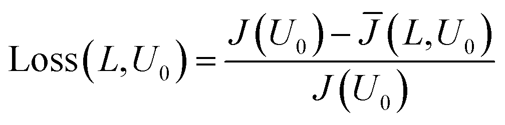 | (10) |
 | ||
| Fig. 4 Effective current density results for various electrode sizes using Tilley2010 (Fe2O3), Kim2013 (Fe2O3), Brillet2012 (WO3) and Kim2016 (BiVO4) datatsets.11,23,24,51 | ||
The current loss initially rises for increasing boundary electrode potential U0 as shown in Fig. 5. The loss drops to a minimum before rising again at potentials where dark current dominates. This effect could be exploited by operating in this minimum region. It is important to note that this loss minimum is not observed with Bulter–Volmer/Tafel type kinetics which have been previously used to study electrode substrate distribution.37,38
 | ||
| Fig. 5 Current losses at various electrode widths for Tilley2010 (Fe2O3), Kim2013 (Fe2O3), Brillet2012 (WO3) and Kim2016 (BiVO4) datatsets.11,23,24,51 | ||
Whilst the overall trend is the same for all the datasets considered, some datasets exhibit a greater difference between the minima and maxima of the loss curves. This is due to the fact that the flatter the slope in the photo-current response at higher potentials, the greater the loss reduction effect. This can be seen when comparing the data for Fe2O3, where the gradient of the current response in the region shortly before dark current is observed is greater for Kim2013 than that of Tilley2010, and hence the current loss minima is more pronounced for Tilley2010. For Brillet2012 and Kim2016 datasets, the dark current isn’t modelled as it is not observed in the potential range of the experimental data. Therefore, they do not display the current loss increase at potentials corresponding to the dark current when compared to those seen Tilley2010 and Kim2013, as shown in Fig. 5.
As analysis was carried out with multiple metal oxide materials, the results demonstrate that the scalability of TCOs is limited by the low conductivity regardless of the semiconductor material used, as any material that performs better than those studied here will incur higher resistive losses.
Solar concentration has been proclaimed as a convenient method of intensifying the process and reducing device costs7,58 and current losses will be increased for future state of the art electrodes operating at higher current densities, as will concentration of solar irradiance with current electrode performance. In order to investigate the latter, the photo-current is assumed to scale linearly with irradiance, an assumption that for hematite has recently been shown to be valid up to 25 suns.59 Furthermore, it was assumed that the increase in concentration of solar irradiance does not change the conductivity of the FTO (e.g. no temperature change on solar concentration). Fig. 6 shows the logarithmic dependence of losses with number of suns which demonstrates that for even mild concentration of light, substrate performance may quickly become an issue.
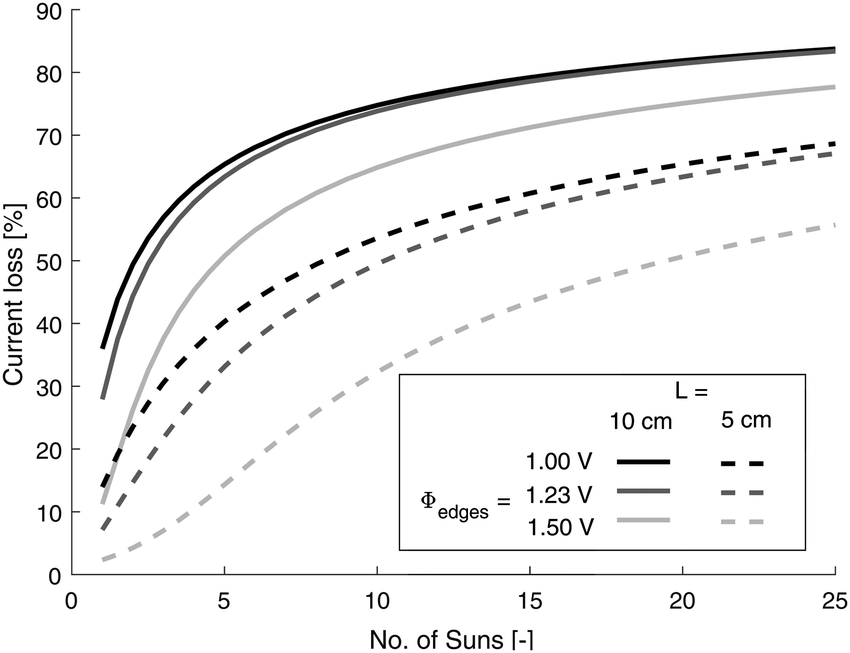 | ||
| Fig. 6 Dependence of effective current loss on number of suns irradiance using Tilley2010 data (Fe2O3). | ||
Whilst reducing current losses is desirable, the predominant aim is to maximise the total system efficiency which appears to be the key driver in economic viability.7,8 A definition for overall system efficiency or total input Energy-To-Hydrogen efficiency (ηETH) is given in eqn (11) and is consistent with definitions previously reported.10,46,60 It is important to note that here, the system level efficiency ηETH is discussed, rather than the diagnostic metrics specific to photo-electrode performance such as Applied-Bias Photon-to-current Efficiency (ABPE), in order to demonstrate the value of minimising substrate resistive losses. Reducing current losses due to substrate potential drop through operation at the ‘minima potential’ requires the potential to be greater than the maximum point potential (see work by Coridan et al.60). This in turn may reduce the overall system efficiency, at a larger bias. If the cell is externally unbiased (Pbias = 0) and ‘self-biased’ by coupling with another photo-electrode or photo-voltaic junction, the operation point will be constrained by the i–v curves of the other subcells. Therefore, the issue of substrate performance for a particular subcell, may subsequently influence the design of the whole system, as subcells in series must be matched in current. Any additional photo-voltage required in order to minimise current losses will change the optimal bandgaps of the system of photo-absorbers, which in turn will impact its efficiency.
For a particular scaled up design, a full assessment of system efficiency that includes the effects of substrate resistivity would be required in order to assess the optimum potential for operation (which may differ from the ideal maximum power point potential).
 | (11) |
4.1 Strategies for scaling up photo-electrodes
In order to design PEC devices of commercially significant areas, the impact of substrate conductivity on device performance must be minimised. Future work may pursue the following routes to achieve this.However these methods have very significant drawbacks. Firstly, creating expansive areas (km2) which capture sufficient solar radiation to produce an economically meaningful amount of fuel from many small area devices (cm2) poses a significant challenge to scale up, as mentioned by Newman.5 Secondly, operating at low current density limits the Energy-To-Hydrogen efficiency and subsequently, if no external power is used, the Solar-To-Hydrogen efficiency.
As this work has demonstrated the significant problems of low performing substrates with current densities of approximately 40 A m−2, a system operating at the 10% Solar-To-Hydrogen (81 A m−2 for Plight = 1000 W m−2) efficiency target for commercialisation7,16 will suffer catastrophic current losses for a single (non-stacked) electrode. One way to circumvent such large current densities would be to stack multiple electrodes in the path of the light as previously discussed in our earlier work.10 This would also permit the use of multiple photo-electrode materials with different bandgaps for a broader capture of the solar spectrum.11
A hybrid substrate approach would involve the use of two materials: FTO and a highly conductive material such as gold or silver. The gold would be deposited in thin lines in a manner similar to back contacts in the photo-voltaic field. This methodology has received very little attention in the field of photo-electrochemistry (briefly discussed by Farivar38 and demonstrated by Lee et al.61), although this methodology has been previously demonstrated for dye sensitised solar cells62,63 and thin film solar cell modules.34 For highly nano-structured photo-anodes, the highly conductive material could come into contact with the electrolyte and hence could be oxidised through participation in electrochemical reaction, thus not many materials would be suitable. Gold has an appropriate potential range in which it is stable as opposed to other materials such as silver. In the work of Lee et al.,61 the Ag grid was encapsulated with epoxy for stability which compromises the available surface area for improved charge collection. This hybrid substrate approach would potentially be extremely scalable but complex to manufacture and there is currently some difficulty in metallizing TCOs.
Furthermore, the current loss is still heavily dependant on the size of the electrode. This means this approach could be used in tandem with the other strategies discussed above. We believe a combination of operation at the plateau in the photo-current response curve and use of hybrid substrates would be an effective way to ensure that current loss due to substrate voltage drop does not limit scale up in FTO based photo-electrodes.
5 Conclusions
The previous work in this field investigating the effect of substrate performance on the photo-electrode performance has been reviewed alongside various methods of modelling the photo-response. A fitted model of the intrinsic current–potential relationship was found to be an accurate and uncomplicated method of capturing the photo-electrode behaviour. Example data for typical metal oxides (Fe2O3, WO3 and BiVO4) was used to quantify the potential drop and current density losses for various substrate geometries (5–50 cm square side length).The ramifications of the numerical results are discussed and at a particular electrode potential the loss of current, due to substrate performance, was minimised. This was found to be a consequence of the complex relationship between the photo-electrode potential and the current which could be exploited by device operation at electrode potentials corresponding to this minimum. The same analysis was performed for concentration of irradiance through linear extrapolation of photo-current response which demonstrated that for even low multiplications of the solar spectrum, substrate performance quickly becomes limiting.
In this work we give no broad heuristic for limiting electrode size as it has been shown that this depends on the complex relationship of the photo-response (which is material dependant). Furthermore, a full economic analysis would be required to assess the extent to which losses are allowable and the optimum electrode potential at which to operate. Crucially this potential may differ from the ideal ‘maximum power point’ potential (see Coridan et al.60). As previously discussed, the economics appear to be sensitive to system efficiency7,8 and therefore future work on the scale up of photo-electrochemical processes, which employ low conductivity substrate such as transparent conductive oxides, will need to take the substrate performance into consideration, especially when intensification through solar concentration is employed.
Nomenclature
| A | Fitted parameter [A m−2] |
| A surface | Photo-electrode geometric surface area [m2] |
| B | Fitted parameter [A m−2] |
| C | Fitted parameter [V vs. RHE] |
| D | Fitted parameter [—] |
| E | Fitted parameter [—] |
| E | Electric field [V m−1] |
| F | Fitted parameter [A m−2] |
| G | Fitted parameter [V−1] |
| G f,H2 | Gibbs free energy of H2 formation [J mol−1] |
| J | Photo-electrode current density [A m−2] |
|
| Average photo-electrode current density [A m−2] |
| J | Current density vector [A m−2] |
| J 0 | Exchange current density [A m−2] |
| J BV | Current density given by Bulter–Volmer [A m−2] |
| J dark | Dark current [A m−2] |
| J photo | Photo-current [A m−2] |
| L | Side length of square [m] |
| L z | Substrate thickness [m] |
| n | Unit normal vector [—] |
| P light | Solar irradiance power [W] |
| P bias | External bias power used [W] |
| P other | Other power added to system [W] |
| Q | Current sources/sinks [A m−3] |
| S | No. of suns [—] |
| S 0 | No. of sun under which experiment was conducted (= 1 sun) [—] |
| U | Electrode potential [V vs. RHE] |
| U 0 | Boundary electrode potential [V vs. RHE] |
| U eq | Equilibrium electrode potential [V vs. RHE] |
| β a | Anodic tafel coefficient [V−1] |
| β c | Cathodic tafel coefficient [V−1] |
| η ETH | Energy-to-hydrogen efficiency [—] |
| η STH | Solar-to-hydrogen efficiency [—] |
| ρ | Bulk resistivity [Ω m] |
| σ | Conductivity [S m−1] |
| Φ | Electric potential [V] |
| Φ 0 | Boundary electric potential [V] |
| Φ electrolyte | Electrolyte electric potential [V] |
| φ H2 | Molar H2 production rate [mol s−1] |
Conflicts of interest
There are no conflicts to declare.References
- J. W. Ager, M. R. Shaner, K. A. Walczak, I. D. Sharp and S. Ardo, Energy Environ. Sci., 2015, 8, 2811–2824 CAS.
- K. Sivula and R. van de Krol, Nat. Rev. Mater., 2016, 1, 15010 CrossRef CAS.
- M. G. Walter, E. L. Warren, J. R. McKone, S. W. Boettcher, Q. Mi, E. A. Santori and N. S. Lewis, Chem. Rev., 2010, 110, 6446–6473 CrossRef CAS PubMed.
- J. R. McKone, N. S. Lewis and H. B. Gray, Chem. Mater., 2014, 26, 407–414 CrossRef CAS.
- J. Newman, J. Electrochem. Soc., 2013, 160, F309–F311 CrossRef CAS.
- T. Bosserez, J. Rongé, J. van Humbeeck, S. Haussener and J. Martens, Oil Gas Sci. Technol., 2015, 70, 877–889 CrossRef CAS.
- B. A. Pinaud, J. D. Benck, L. C. Seitz, A. J. Forman, Z. Chen, T. G. Deutsch, B. D. James, K. N. Baum, G. N. Baum, S. Ardo, H. Wang, E. Miller and T. F. Jaramillo, Energy Environ. Sci., 2013, 6, 1983–2002 CAS.
- P. Zhai, S. Haussener, J. Ager, R. Sathre, K. Walczak, J. Greenblatt and T. McKone, Energy Environ. Sci., 2013, 6, 2380 CAS.
- M. E. Orazem and J. Newman, J. Electrochem. Soc., 1984, 131, 2582–2588 CrossRef CAS.
- I. Holmes-Gentle, F. Hoffmann, C. A. Mesa and K. Hellgardt, Sustainable Energy Fuels, 2017, 1, 1184–1198 CAS.
- J. H. Kim, J.-W. Jang, Y. H. Jo, F. F. Abdi, Y. H. Lee, R. van de Krol and J. S. Lee, Nat. Commun., 2016, 7, 13380 CrossRef CAS PubMed.
- O. Khaselev and J. A. Turner, Science, 1998, 280, 425–427 CrossRef CAS PubMed.
- T. J. Jacobsson, V. Fjällström, M. Sahlberg, M. Edoff and T. Edvinsson, Energy Environ. Sci., 2013, 6, 3676 CAS.
- A. Nakamura, Y. Ota, K. Koike, Y. Hidaka, K. Nishioka, M. Sugiyama and K. Fujii, Appl. Phys. Express, 2015, 8, 107101 CrossRef.
- J. Jia, L. C. Seitz, J. D. Benck, Y. Huo, Y. Chen, J. W. D. Ng, T. Bilir, J. S. Harris and T. F. Jaramillo, Nat. Commun., 2016, 7, 13237 CrossRef CAS PubMed.
- R. van de Krol and M. Grätzel, Photoelectrochemical Hydrogen Production, Springer, 2012, vol. 102 Search PubMed.
- Z. Chen, H. N. Dinh and E. Miller, Photoelectrochemical Water Splitting, Springer New York, New York, NY, 2013 Search PubMed.
- S. M. Sze and K. K. Ng, Physics of Semiconductor Devices, John Wiley & Sons, 2006 Search PubMed.
- M. G. Helander, M. T. Greiner, Z. B. Wang, W. M. Tang and Z. H. Lu, J. Vac. Sci. Technol., A, 2011, 29, 011019 Search PubMed.
- E. R. Batista and R. A. Friesner, J. Phys. Chem. B, 2002, 106, 8136–8141 CrossRef CAS.
- S.-E. Lindquist, B. Finnström and L. Tegner, J. Electrochem. Soc., 1983, 130, 351–358 CrossRef CAS.
- Y. Liang, T. Tsubota, L. P. A. Mooij and R. van de Krol, J. Phys. Chem. C, 2011, 115, 17594–17598 CAS.
- J. Y. Kim, G. Magesh, D. H. Youn, J.-W. Jang, J. Kubota, K. Domen and J. S. Lee, Sci. Rep., 2013, 3, 2681 CrossRef PubMed.
- S. D. Tilley, M. Cornuz, K. Sivula and M. Grätzel, Angew. Chem., Int. Ed., 2010, 49, 6405–6408 CrossRef CAS PubMed.
- A. Kay, I. Cesar and M. Grätzel, J. Am. Chem. Soc., 2006, 128, 15714–15721 CrossRef CAS PubMed.
- M. Ibadurrohman and K. Hellgardt, Int. J. Hydrogen Energy, 2014, 39, 18204–18215 CrossRef CAS.
- A. J. Cowan, C. J. Barnett, S. R. Pendlebury, M. Barroso, K. Sivula, M. Grätzel, J. R. Durrant and D. R. Klug, J. Am. Chem. Soc., 2011, 133, 10134–10140 CrossRef CAS PubMed.
- J. K. Kim, K. Shin, S. M. Cho, T.-W. Lee and J. H. Park, Energy Environ. Sci., 2011, 4, 1465 CAS.
- C. Santato, M. Ulmann and J. Augustynski, J. Phys. Chem. B, 2001, 105, 936–940 CrossRef CAS.
- C. Ong, S. Dennison, S. Fearn, K. Hellgardt and G. Kelsall, Electrochim. Acta, 2014, 125, 266–274 CrossRef CAS.
- W. Li, J. Li, X. Wang, S. Luo, J. Xiao and Q. Chen, Electrochim. Acta, 2010, 56, 620–625 CrossRef CAS.
- X. Wen, S. Wang, Y. Ding, Z. L. Wang and S. Yang, J. Phys. Chem. B, 2005, 109, 215–220 CrossRef CAS PubMed.
- P. Tang, H. Xie, C. Ros, L. Han, M. Biset-Peiró, Y. He, W. Kramer, A. P. Rodríguez, E. Saucedo, J. R. Galán-Mascarós, T. Andreu, J. R. Morante and J. Arbiol, Energy Environ. Sci., 2017, 10, 2124–2136 CAS.
- M. W. Rowell and M. D. McGehee, Energy Environ. Sci., 2011, 4, 131–134 CAS.
- E. Fortunato, D. Ginley, H. Hosono and D. C. Paine, MRS Bull., 2007, 32, 242–247 CrossRef CAS.
- A. Shah, H. Schade, M. Vanecek, J. Meier, E. Vallat-Sauvain, N. Wyrsch, U. Kroll, C. Droz and J. Bailat, Prog. Photovoltaics Res. Appl., 2004, 12, 113–142 CrossRef CAS.
- C. Carver, Z. Ulissi, C. Ong, S. Dennison, G. Kelsall and K. Hellgardt, Int. J. Hydrogen Energy, 2012, 37, 2911–2923 CrossRef CAS.
- F. Farivar, Int. J. Hydrogen Energy, 2016, 41, 882–888 CrossRef CAS.
- W. W. Gärtner, Phys. Rev., 1959, 116, 84 CrossRef.
- J. Reichman, Appl. Phys. Lett., 1980, 36, 574 CrossRef CAS.
- R. Memming, Semiconductor Electrochemistry, Wiley-VCH-Verl, Weinheim, 2nd edn, 2015, p. 470 Search PubMed.
- K. Rajeshwar, Encyclopedia of Electrochemistry, Wiley, 2002, vol. 6 Search PubMed.
- H. Döscher, J. F. Geisz, T. G. Deutsch and J. A. Turner, Energy Environ. Sci., 2014, 7, 2951–2956 Search PubMed.
- L. M. Peter, J. Solid State Electrochem., 2013, 17, 315–326 CrossRef CAS.
- K. Upul Wijayantha, S. Saremi-Yarahmadi and L. M. Peter, Phys. Chem. Chem. Phys., 2011, 13, 5264 RSC.
- A. Hankin, F. E. Bedoya-Lora, C. K. Ong, J. C. Alexander, F. Petter and G. H. Kelsall, Energy Environ. Sci., 2017, 10, 346–360 CAS.
- Y. He, I. M. Gamba, H.-C. Lee and K. Ren, SIAM J. Appl. Math., 2015, 75, 2515–2539 CrossRef.
- M. Harmon, I. M. Gamba and K. Ren, 2016, arXiv preprint arXiv:1604.07855.
- Y. K. Gaudy and S. Haussener, J. Mater. Chem. A, 2016, 4, 3100–3114 CAS.
- H. Nalwa, Handbook of Thin Film Materials: Semiconductor and Superconductor Thin Films, Academic Press, 2002 Search PubMed.
- J. Brillet, J.-H. Yum, M. Cornuz, T. Hisatomi, R. Solarska, J. Augustynski, M. Grätzel and K. Sivula, Nat. Photonics, 2012, 6, 824–828 CrossRef CAS.
- J. H. Kennedy and K. W. Frese, J. Electrochem. Soc., 1978, 125, 709–714 CrossRef CAS.
- M. V. C. Sastri and G. Nagasubramanian, Int. J. Hydrogen Energy, 1982, 7, 873–876 CrossRef CAS.
- H. P. Maruska and A. K. Ghosh, Sol. Energy Mater., 1979, 1, 237–247 CrossRef CAS.
- M. A. Butler, J. Appl. Phys., 1977, 48, 1914 CrossRef CAS.
- M. A. Modestino, S. M. H. Hashemi and S. Haussener, Energy Environ. Sci., 2016, 9, 1533–1551 CAS.
- A. Rohatgi, WebPlotDigitizer, Version: 4.0, Austin, Texas, USA, 2017, https://automeris.io/WebPlotDigitizer Search PubMed.
- M. Dumortier, S. Tembhurne and S. Haussener, Energy Environ. Sci., 2015, 8, 3614–3628 CAS.
- G. Segev, H. Dotan, K. D. Malviya, A. Kay, M. T. Mayer, M. Grätzel and A. Rothschild, Adv. Energy Mater., 2016, 6, 1500817 CrossRef.
- R. H. Coridan, A. C. Nielander, S. A. Francis, M. T. McDowell, V. Dix, S. M. Chatman and N. S. Lewis, Energy Environ. Sci., 2015, 8, 2886–2901 CAS.
- W. J. Lee, P. S. Shinde, G. H. Go and E. Ramasamy, Int. J. Hydrogen Energy, 2011, 36, 5262–5270 CrossRef CAS.
- W. J. Lee, E. Ramasamy, D. Y. Lee and J. S. Song, Sol. Energy Mater. Sol. Cells, 2007, 91, 1676–1680 CrossRef CAS.
- R. Escalante, D. Pourjafari, D. Reyes-Coronado and G. Oskam, J. Renewable Sustainable Energy, 2016, 8, 023704 CrossRef.
| This journal is © the Owner Societies 2018 |