
 Open Access Article
 This Open Access Article is licensed under a
 Creative Commons Attribution 3.0 Unported Licence
Surface structure, optoelectronic properties and charge transport in ZnO nanocrystal/MDMO-PPV multilayer films†
Qing
Lian
a,
Mu
Chen
a,
Muhamad Z.
Mokhtar
a,
Shanglin
Wu
a,
Mingning
Zhu
a,
Eric
Whittaker
b,
Paul
O’Brien
 ac and
Brian R.
Saunders
*a
ac and
Brian R.
Saunders
*a
aSchool of Materials, University of Manchester, MSS Tower, Manchester, M13 9PL, UK. E-mail: Brian.saunders@manchester.ac.uk
bPhoton Science Institute, University of Manchester, Alan Turing Building, Oxford Road, Manchester, M13 9PL, UK
cSchool of Chemistry, University of Manchester, Manchester, M13 9PL, UK
First published on 17th April 2018
Abstract
Blends of semiconducting nanocrystals and conjugated polymers continue to attract major research interest because of their potential applications in optoelectronic devices, such as solar cells, photodetectors and light-emitting diodes. In this study we investigate the surface structure, morphological and optoelectronic properties of multilayer films constructed from ZnO nanocrystals (NCs) and poly[2-methoxy-5-(3′,7′-dimethyloctyloxy)-1,4-phenylenevinylene] (MDMO-PPV). The effects of layer number and ZnO concentration (CZnO) used on the multilayer film properties are investigated. An optimised solvent blend enabled well-controlled layers to be sequentially spin coated and the construction of multilayer films containing six ZnO NC (Z) and MDMO-PPV (M) layers (denoted as (ZM)6). Contact angle data showed a strong dependence on CZnO and indicated distinct differences in the coverage of MDMO-PPV by the ZnO NCs. UV-visible spectroscopy showed that the MDMO-PPV absorption increased linearly with the number of layers in the films and demonstrates highly tuneable light absorption. Photoluminescence spectra showed reversible quenching as well as a surprising red-shift of the MDMO-PPV emission peak. Solar cells were constructed to probe vertical photo-generated charge transport. The measurements showed that (ZM)6 devices prepared using CZnO = 14.0 mg mL−1 had a remarkably high open circuit voltage of ∼800 mV. The device power conversion efficiency was similar to that of a control bilayer device prepared using a much thicker MDMO-PPV layer. The results of this study provide insight into the structure–optoelectronic property relationships of new semiconducting multilayer films which should also apply to other semiconducting NC/polymer combinations.
Introduction
Hybrid nanocrystal (NC)/polymer composites contain semiconducting inorganic NCs (or quantum dots) dispersed within a conjugated polymer matrix.1–5 They continue to attract considerable activity from both the fundamental6–9 and practical perspectives.10,11 Potential applications for such composites include solar cells,12,13 photodetectors14,15 or light emitting diodes.16 Unfortunately, the intrinsic lack of colloidal stability during composite formation is an obstacle that frustrates efforts to obtain high efficiency semiconducting NC/polymer solar cells.17 This instability prevents attainment of a controlled network of connected NCs dispersed throughout the conjugated polymer phase.18 Very small separations between connected strings of NCs are required to maximise the exciton diffusion yield because the exciton diffusion length for conjugated polymers is typically less than 10 nm.19 The power conversion efficiencies (PCEs) for NC/polymer solar cells remain relatively low compared to comparable technologies such as polymer–fullerene solar cells20 despite elegant approaches designed to circumvent the colloidal instability problem.2,17,21 Here, we aimed to introduce a degree of tuneable order perpendicular to the film plane within semiconducting NC/polymer composites. Such composites utilised multilayer films with polymer layer thicknesses less than the exciton diffusion length. The surface structures and morphologies of the multilayer films are studied to understand their influence on the optoelectronic properties of the films and photo-generated charge transport in the z-direction. A practical question addressed is whether operational solar cells could be achieved using such semiconducting multilayer NC/polymer films.ZnO NCs were used as the model semiconducting NC system in this study. They can be conveniently prepared using a solvothermal method22 or chemical vapor deposition23 and have been reviewed elsewhere.24,25 ZnO has a large band gap (∼3.2 eV), a very high electron mobility and is an electron acceptor.25,26 The ZnO NC/polymer solar cells with the highest PCE reported are those in seminal work from the Janssen group.17 They used in situ ZnO NC preparation during film formation to bypass colloidal instability obstacles. However, there are two challenges present for in situ NC formation within composite films which are lack of control over NC size and placement. Other approaches that provided structural control within ZnO NC/polymer composites include using pre-formed ZnO nanorods26 or porous ZnO NC films.27 Whilst these approaches may allow well-defined vertical pathways to be established for electron transport, infiltration of the polymer into the spaces can be hindered if the latter are very small.28 Here, we aimed to retain NC colloidal stability whilst precisely controlling the location of the NC and polymer components in multilayer films using sequential spin coating.
Whilst ZnO NCs have been studied for decades22,29 their use in multilayer composite films has received less attention. Such films have mainly been studied within bespoke tandem and multilayer solar cells30–34 with component energy levels carefully selected to maximise the PCE. The approach used in the present study is depicted in Scheme 1. Multilayer films were constructed by sequentially spin coating layers of ZnO NCs (denoted as Z) and poly[2-methoxy-5-(3′,7′-dimethyloctyloxy)-1,4-phenylenevinylene] (MDMO-PPV, denoted as M). MDMO-PPV was used at the donor in this study because earlier studies showed the photoluminescence behaviour for ZnO NC/MDMO-PPV films to be well controlled by the proportion of each species.29 Our multilayer films consisted of one type of polymer donor and NC acceptor with a repeating bilayer (heterojunction) structure. This design simplified the study and enabled a clearer understanding of the structure–optoelectronic properties to be discerned. Multilayer films with up to six Z and M layers (i.e., (ZM)6) were constructed. Our multilayer films were not designed to provide high PCE devices. Rather, we employed solar cell measurements to study the effect of ZnO NC layer thickness on vertical photo-generated charge transport via the short-circuit current density (see later).
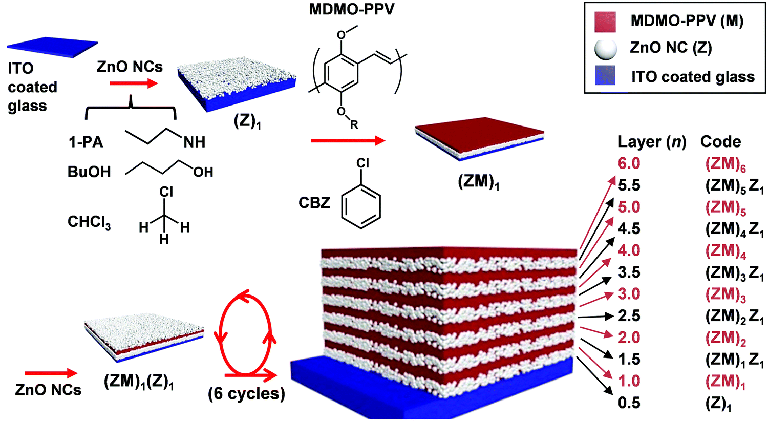 | ||
| Scheme 1 Depiction of preparation of ZnO NC/MDMO-PPV multilayer films. Each layer was formed by spin coating a ZnO NC dispersion or a MDMO-PPV solution. (ZM)n and (ZM)n(Z)1 (where n = 1 to 6) correspond to multilayer films that contain MDMO-PPV or ZnO NCs as the top layer, respectively. The parameter n is the number of bilayers. | ||
The study begins with establishing a solvent-blend which gave colloidally stable ZnO NC dispersions that did not adversely affect the underlying MDMO-PPV layers when spin coated. Multilayer films are then constructed and characterised using surface profilometry (for layer thickness), SEM, AFM as well as contact angle measurements. The optical properties of the films are investigated using UV-visible and photoluminescence (PL) spectroscopy. Solar cell data are then considered and the effect of ZnO film layer thickness studied. The latter data provide evidence for vertical charge transport pathways through the multilayer films. Finally, all of the results are considered to propose structural models of the multilayer films. The sequential spin coating method established here for ZnO NC/MDMO-PPV multilayer films provides optoelectronic properties that are tuneable using the number of layers and NC concentration. Our approach and the results obtained should be applicable to a range of other semiconducting NC/conjugated polymer films or devices.
Experimental details
Materials
Zinc acetate dihydrate (Zn(Ac)2·2H2O, 98%), KOH (85%), methanol (MeOH, 99.8%), butanol (BuOH, >99%), CHCl3 (99.8%), chlorobenzene (CBZ, anhydrous, 99.8%) and MDMO-PPV (Mn ∼ 120![[thin space (1/6-em)]](https://www.rsc.org/images/entities/char_2009.gif) 000 g mol−1) were purchased from Sigma-Aldrich. 1-Propylamine (1-PA, >99%) and isopropanol (IPA, anhydrous, 99.5%) were purchased from Alfa Aesar. All of the above materials were used as received. Ultrahigh purity water (distilled and deionised) was used in all experiments.
000 g mol−1) were purchased from Sigma-Aldrich. 1-Propylamine (1-PA, >99%) and isopropanol (IPA, anhydrous, 99.5%) were purchased from Alfa Aesar. All of the above materials were used as received. Ultrahigh purity water (distilled and deionised) was used in all experiments.
ZnO nanocrystals synthesis
ZnO NCs were synthesised following the method reported previously.29 Briefly, Zn(Ac)2·2H2O (2.95 g, 13.4 mmol) was dissolved in MeOH (125 mL) and heated to 60 °C. Then a solution of KOH (1.51 g, 18.6 mmol) in MeOH (65 mL) was slowly added over 10 min with vigorous stirring. After 5 min the solution became translucent and the stirring was continued for 150 min. Finally, the ZnO NCs were washed twice with MeOH, collected by centrifuge and re-suspended in hexane. The purified NC dispersion was stored at −18 °C until use.Multilayer film preparation
A BuOH/CHCl3/1-PA solvent blend (volume ratio of 5:1:1) was used to disperse the ZnO NCs. The 1-PA acted as a ligand.27,29 The ZnO NC dispersion was filtered through a 0.01 um PTFE syringe filter before use. The ZnO NC concentrations (CZnO) used in this study were in the range of 5.0 to 28.0 mg mL−1. Spin-coating was performed using pre-cleaned glass substrates (∼2.0 × 1.5 cm2) or ITO-coated glass substrates (20 Ω sq−1). The latter were cleaned by sonication in a 1% Hellmanex solution, rinsed with IPA, water and then dried. Spin-coating was conducted using a Laurell, Model WS-650Mz-23NPP spin-coater. First, a ZnO NC layer was spin-coated using NCs dispersed in the solvent blend (50 μL) onto the ITO glass (2000 rpm, 1.0 min). A MDMO-PPV solution in CBZ (50 μL, 3.0 mg mL−1) was then spin coated on top of the ZnO NC layer (2000 rpm, 1.0 min) to give a (ZM)1 film (Scheme 1). These steps were repeated to construct multilayer films ((denoted ZM)n, n ≤ 6). All films were stored in a vacuum chamber or a nitrogen filled glove box.
Solar cell fabrication
The patterned ITO glass (Ossila Ltd UK) was ultrasonically cleaned for 30 min in 1% Hellmanex III solution, IPA and then aqueous NaOH solution (2.5 M). Finally, the patterned ITO glass was extensively washed with water and dried under a N2 gas stream and annealed on a hotplate as described below. The process of multilayer (ZM)6 film preparation used was the same as that described above. A PEDOT:PSS solution (100 μL, 1.3 wt% in water) was spin coated on top of the final MDMO-PPV layer at 4000 rpm at 90 °C. The film was then annealed at 100 °C for 10 min on a hotplate. The thickness of PEDOT:PSS layer was ∼100 nm. An Au layer (80 nm) was deposited on top of the PEDOT:PSS layer to complete the device.A bilayer control device was prepared with 1 ZnO and MDMO-PPV layer (i.e., (ZM)1) using CZnO = 28.0 mg mL−1. MDMO-PPV solution in CBZ (6.0 mg mL−1) was spin coated onto the ZnO layer at 2000 rpm. The thickness of the MDMO-PPV layer was 51 nm. PEDOT:PSS (100 μL) was then spin coated on top of the MDMO-PPV layer and annealed and Au deposited as described above.
Physical measurements
Dynamic light scattering (DLS) was conducted using a 50 mW He/Ne laser operated at 633 nm with a standard avalanche photodiode and 90° detection optics connected to a Malvern Zetasizer Nano ZS90 autocorrelator. SEM was performed using FEI Quanta 650 FEG-SEM and FEI Magellan 400 XHR FEG-SEM instrument. The samples were coated with Pt. TEM data were obtained using an FEI Tecnai F30 FEG-AEM instrument. The samples were deposited onto holy carbon film from Agar Scientific. Atomic force microscopy (AFM) images were obtained with an Asylum Research MFP-3D operating in AC (“tapping”) mode. Imaging was performed using an Olympus high aspect ratio etched silicon probes (OTESPA) with a nominal spring constant of 42 N m−1 (Bruker AXS S.A.S., France). The cantilever oscillation frequency varied between 300 and 350 kHz and was determined by the auto-tune facility of the Asylum software, as was the drive amplitude. The thickness of the films was measured using a DektakXT profilometer. Contact angle measurements were performed using water and a Krüss Drop Shape Analysis (DSA100) instrument. All contact angle measurements were performed at room temperature. UV-visible spectra were obtained by using a Hitachi U-1800 spectrophotometer. PL spectra were measured using a double monochromator FLS980 instrument (Edinburgh Instruments, UK), which was equipped with a xenon lamp and detector (R928.0P, Hamamatsu). The excitation wavelength was 505 nm.Device measurements
The current density–voltage (J–V) characteristics were measured using a Keithley 2420 Sourcemeter and 100 mW cm−2 illumination (AM 1.5G) together with a calibrated NREL certified Oriel Si-reference cell. An Oriel SOL3A solar simulator was used for these experiments. The active area of the devices was defined using a square aperture within a mask and fixed at 0.025 cm2. The scan rate was 100 mV s−1.Results and discussion
Multi-layer film morphology and surface hydrophilicity/hydrophobicity switching
It was important to use a solvent blend that provided colloidally stable ZnO NCs to enable deposition of well-controlled multilayer films by spin coating. A further goal for the solvent blend was that it should not dissolve the underlying MDMO-PPV layer. A preliminary study was conducted using a range of solvents. Finally, a BuOH, CHCl3 and 1-PA solvent blend (volume ratio of 5:1:1) was selected for dispersing the ZnO NCs. The solvent blend maintained NC colloidal stability and minimised MDMO-PPV dissolution. TEM images obtained for the ZnO NCs (see Fig. S1(a), ESI†) gave a number-average diameter (dTEM) of 4.1 ± 0.4 nm. A UV-visible spectrum measured for the dispersed NCs (see Fig. S1(b), ESI†) gave a wavelength at which the absorption is half that of the excitonic peak (λ1/2) of 360 nm. This value enabled the NC diameter to be calculated as 4.9 nm following Meulenkamp's method.22 DLS data were also obtained (see Fig. S1(c), ESI†) which showed a monomodal size distribution and gave a mean (z-average) diameter (dz) of 13 nm. The relatively large dz value is due to 1-PA adsorbed to the ZnO NCs and the disproportionately strong scattering of light by larger particles that is a characteristic of DLS.35
Multilayer films were constructed using sequential spin coating of ZnO NC and MDMO-PPV solutions (Scheme 1). The first layer deposited was ZnO NCs (i.e., (Z)1). Then an MDMO-PPV layer was spin coated on top of the ZnO NC layer to give a bilayer film (i.e., (ZM)1). The process was repeated to build up multilayer films ((ZM)n). CBZ was used as the solvent for MDMO-PPV because it did not re-disperse the underlying ZnO NC layer during spin coating of the MDMO-PPV layer. The effects of CZnO (=5.0, 9.0 and 28.0 mg mL−1) and numbers of bilayers (n) on the overall thickness of the multilayer films was studied (see Fig. 1(a)). The multilayer films prepared using all three CZnO values exhibited a linear increase of thickness with increasing n. However, the multilayer films prepared using CZnO = 28.0 mg mL−1 showed a step sequence. This trend is because the ZnO NC layers were much thicker than the MDMO-PPV layers for this film (discussed below).
 | ||
| Fig. 1 (a) Variation of overall thickness of ZnO NC/MDMO-PPV multilayer films prepared using CZnO = 5.0, 9.0 and 28.0 mg mL−1 with number of bilayers (n). The top layer of the (ZM)n films was MDMO-PPV. The top layer of the (ZM)n(Z)1 films was ZnO. The numbers in square brackets are CZnO. (b) Calculated layer thickness (= tL(n) − tL(n−0.5), where n = 0.5 to 6.0) for the three multilayer films. (c) Variation of the average layer thickness with CZnO. Data are also shown for one ZnO NC layer (i.e., (Z)1) deposited on ITO for comparison and are taken from Fig. S2 (ESI†). | ||
The ZnO NC or MDMO-PPV layer thickness (tL) was calculated from the difference of the overall thicknesses of a given layer and that of the preceding layer (see Fig. 1(b)). These data show that the tL values for the ZnO NC films approach those for the MDMO-PPV layers as CZnO decreases. The average MDMO-PPV tL value calculated from the data shown in Fig. 1(b) are plotted in Fig. 1(c) for each CZnO used. Clearly, the average MDMO-PPV layer thickness was independent of CZnO. The average thickness of all of the MDMO-PPV layers (i.e., all the red data points in Fig. 1(b)) was 6.0 ± 1.4 nm. For comparison, the thickness of a single film of MDMO-PPV spin coated on ITO glass was measured as 10 ± 0.4 nm. This difference can be explained by some of the MDMO-PPV infiltrating the underlying ZnO NC layers and/or being removed during spin coating. The diameter of a collapsed spherical MDMO-PPV globule with a molecular weight of 120000 g mol−1 can be shown to be ∼8 nm assuming a density of 0.91 g mL−1.36 Hence, the MDMO-PPV layers can be thought of as monolayers of MDMO-PPV globules.
We next consider the ZnO NC layers. The average ZnO NC layer thickness (i.e., for (ZM)n(Z)1) was 5.1 ± 1.2 nm for the multilayer films prepared using CZnO = 5 mg mL−1 (Fig. 1(b), top). However, the thickness of the ZnO NC layers were larger than that for the MDMO-PPV layers (i.e., (ZM)n) when the CZnO value increased to 9.0 and 28.0 mg mL−1 and “zig-zag” trends were apparent (Fig. 1(b) middle and bottom). The average ZnO NC layer thickness calculated for each of the three multilayer films (from the blue data points in Fig. 1(b)) increased linearly with CZnO (see Fig. 1(c)). It is interesting to compare the latter values with the thicknesses of single ZnO NC films of (i.e., (Z)1) deposited on ITO using the same CZnO values (see Fig. 1(c)). (Additional data for (Z)1 deposited on ITO are shown in Fig. S2, ESI†). These data show that there is no significant difference between the layer thicknesses for ZnO NC layers deposited on ITO and MDMO-PPV layers in the multilayer films. Thus, the ZnO NCs did not become significantly submerged in the underlying MDMO-PPV layers. The ZnO layers within the multilayer films prepared using CZnO = 5.0, 9.0 and 28.0 mg mL−1 can be approximated as ∼1, 2 and 8 ZnO NC monolayers, respectively, from the dTEM value (4.1 nm) and the average ZnO NC layer thicknesses of 5.1, 8.5 and 32.2 nm from Fig. 1(c).
The morphologies for the multilayer films prepared using CZnO = 28.0 mg mL−1 were investigated using SEM and AFM. Selected images measured for the (ZM)3(Z)1, (ZM)4 and (ZM)4(Z)1 films are shown in Fig. 2. (SEM and AFM images were measured for the other layers and are shown in Fig. S3 and S4, respectively, ESI†). The SEM images (Fig. 2(a)–(c)) show that the films that had ZnO NCs as the top layer (i.e., ((ZM)3(Z)1 and (ZM)4(Z)1) had a polycrystalline appearance and many very small troughs (diameter <10 nm) were present. These troughs are highlighted with arrows. The SEM image measured for the (ZM)4 film (MDMO-PPV top layer, Fig. 2(b)) had larger troughs with diameters of 10–20 nm. The AFM images recorded for these films (Fig. 2(d)–(f)) showed similar features to those apparent in the respective SEM images. The line profile data showed that the roughness for the (ZM)4 film (RMS roughness = 1.2 nm) was much less than those for the (ZM)3(Z)1 film (roughness = 2.6 nm) and (ZM)4(Z)1) film (roughness = 2.2 nm). (This trend is also apparent from the AFM images and line profiles measured for the other (ZM)n and (ZM)nZ1 multilayer films – see Fig. S4, ESI†). Hence, the ZnO NC layers ((ZM)n(Z)1)) had a greater roughness than the MDMO-PPV ((ZM)n layers). This is because the former were composed of non-deformable NCs. The subsequent MDMO-PPV layer (for (ZM)n) (mostly) filled in the smaller troughs present in the preceding ZnO NC layer. However, some larger diameter troughs remained that were less deep as judged by the AFM line profile data shown in Fig. 2 and Fig. S4 (ESI†). These features were covered by the next ZnO NC layer, which is why the morphologies repeated as n increased. There was no memory of the preceding (ZM)n−1 or (ZM)n−1(Z)1 layer morphology by the next, respective, (ZM)n or (ZM)n(Z)1 layer. Thus, the surface morphologies for these multilayer films were “reset” after each bilayer cycle.
 | ||
| Fig. 2 SEM images for (a) top ZnO NC layer in (ZM)3(Z)1 (b) top MDMO-PPV layer in (ZM)4 and (c) top ZnO NC layer in (ZM)4(Z)1. These films were prepared using CZnO = 28.0 mg mL−1. The yellow arrows highlight troughs, which had a larger diameter for the (ZM)4 films. AFM images and surface profiles were also measured for these films (labelled) and are shown in (d–f). Scale bars: 100 nm. SEM and AFM for other films are shown in Fig. S3 and S4 (ESI†), respectively. | ||
The hydrophobic and hydrophilic properties of the multilayer film surfaces were investigated using contact angle (CA) measurements. The CA's for MDMO-PPV (i.e., (M)1) and ZnO ((Z)1) deposited on ITO were measured as 95.7° and 33.2°, respectively. The former value agrees closely with the CA reported for MDMO-PPV.37,38 The CA for ZnO has been reported as 10° after exposure to UV light.39,40 This effect is termed photo-induced surface wettability and originates from coordination of H2O to O2 vacancy sites.39Fig. 3(a) shows images of water droplets recorded on several of the multilayer films. Clearly, the droplets spread on the top ZnO layer for (ZM)3(Z)1 and (ZM)4(Z)1. However, the droplets tended de-wet the top MDMO-PPV layer (for (ZM)4). These data show that the ZnO NC and MDMO-PPV layers are hydrophilic and hydrophobic, respectively.
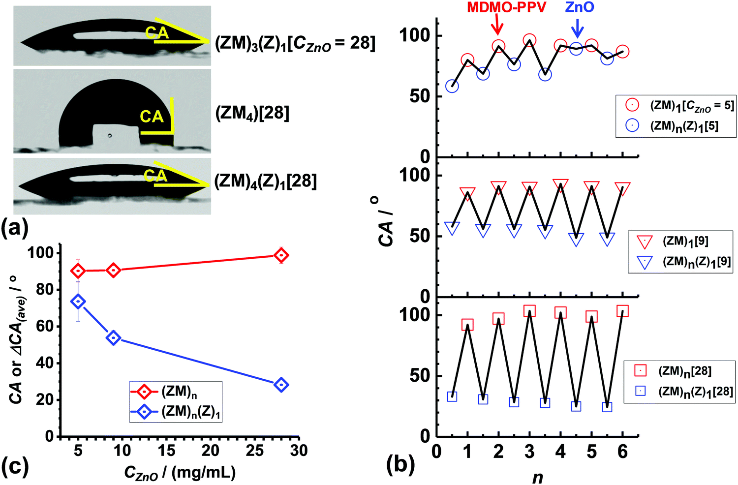 | ||
| Fig. 3 (a) Images obtained of water droplets on multilayer films prepared using CZnO = 28.0 mg mL−1. (b) Contact angles measured for films prepared using CZnO = 5.0 mg mL−1 (top), 9.0 mg mL−1 (middle) and 28.0 mg mL−1 (bottom). (c) Average contact angles for the MDMO-PPV top layer (i.e., (ZM)n) and ZnO NC layers (i.e., (ZM)n(Z)1) films obtained from the data shown in (b). | ||
The CA values measured for each of the layers of the three ZnO NC/MDMO-PPV multilayer films are shown in Fig. 3(b). The data exhibited a “zig-zag” pattern for all of the films which demonstrates that a surface hydrophilicity/hydrophobicity change (switching) occurred with the deposition of each layer. The reversibility of the CA values was reasonably good for the films prepared using CZnO = 9.0 and 28.0 mg mL−1. The data show that for these two multilayer films the surfaces were hydrophilic and hydrophobic for the (ZM)n(Z)1 and (ZM)n layers, respectively. The data for the film prepared using CZnO = 5.0 mg mL−1 (Fig. 3(b), top) showed a different behavior whereby the CA for the ZnO NC layers increased as n increased and approached the values for MDMO-PPV layers. It follows that when the ZnO NCs were deposited for this film the (ZM)n(Z)1 layers had similar hydrophobicity to the underlying (ZM)n layer. This is suggestive of incomplete coverage of the MDMO-PPV layers by the ZnO NCs when CZnO = 5.0 mg mL−1. The average values of the CAs shown in Fig. 3(b) are plotted as a function of CZnO in Fig. 3(c). The average CA values for the (ZM)n layers was independent of CZnO. In contrast the average CA values for the (ZM)n(Z)1 layers decreased with increasing CZnO. It follows that the effectiveness of ZnO NC coverage of the underlying MDMO-PPV layers increased with increasing CZnO.
Optical properties of multilayer films
UV-visible spectra were measured for the ZnO NC/MDMO-PPV multilayer films. The spectra measured for the films prepared using CZnO = 28.0 mg mL−1 are shown in Fig. 4(a). (The spectra obtained for the films prepared using CZnO = 5.0 and 9.0 mg mL−1 are shown in Fig. S5, ESI†). The spectra show an absorption maximum at 505 nm which is due to MDMO-PPV.29 The ZnO NC layers did not strongly contribute to the spectra because ZnO does not absorb above 400 nm (Fig. S1(b), ESI†). The variation of the maximum absorbance with n for the three multilayer films is shown in Fig. 4(b). The film prepared using CZnO = 5 mg mL−1 (Fig. 4(b), top) exhibited a step-like sequence. The film absorbance measured for each ZnO NC top layer (blue data points) was less than that for the preceding MDMO-PPV top layer (red data points). We conclude from this result that some of the MDMO-PPV was removed as a consequence of spin coating of the ZnO NC layers. Generally, this effect was less pronounced for the films prepared using CZnO = 9.0 and 28.0 mg mL−1. | ||
| Fig. 4 (a) UV-visible spectra for ZnO NC/MDMO-PPV multilayer films prepared using CZnO = 28.0 mg mL−1. (b) Variation of absorbance measured at 505 nm with bilayer number for the films prepared using CZnO = 5.0 (top), 9.0 (middle) and 28.0 (bottom) mg mL−1. (c) Absorption coefficient for the films versus CZnO where αexp, αIdeal and αThick were experimentally obtained or those determined using ϕMDM values calculated from eqn (2) and (3), respectively (see text). | ||
The absorption coefficient (α) for the ZnO NC/MDMO-PPV multilayer films was assumed to be proportional to the overall volume fraction of MDMO-PPV present (αMDM) and the absorption coefficient of MDMO-PPV (αMDM).
| α = ϕMDMαMDM | (1) |
The experimental α value (αexp) was determined from the gradient of plots of the absorbance maximum against film thickness (Fig. S6, ESI†). The αexp values are shown in Fig. 4(c). A value of αMDM = 1.3 × 10⁷ m−1 was estimated from the absorbance of the MDMO-PPV film (Fig. 4(a)) and its thickness (10 nm). The latter value is the same as that reported in the literature.29 We calculated ideal absorption coefficients (αIdeal) for the multilayer films using ideal ϕMDM values (ϕMDM(Ideal)) using the assumption that all of the ZnO NCs and MDMO-PPV used to spin coat the films was incorporated. The equation used was
 | (2) |
41) and ZnO (0.91 g mL−136), respectively. The derivation of eqn (2) is given in the ESI.† The values for αIdeal are plotted in Fig. 4(c) and it can be seen that in all cases αIdeal > αexp. This result implies that the experimental ϕMDM value was less than ϕMDM(Ideal). Presumably, some MDMO-PPV was removed during multilayer film construction. We also calculated α values (αThick) using eqn (1) and ϕMDM values estimated from the average thicknesses (ϕMDM(Thick)) of the MDMO-PPV (tMDM) and ZnO layers (tZnO) in the films using | (3) |
Photoluminescence (PL) spectra were also measured for the three ZnO NC/MDMO-PPV multilayer films. The spectra measured for the films prepared using CZnO = 28.0 mg mL−1 appear in Fig. 5(a) and those measured for the films prepared using 5.0 and 9.0 mg mL−1 are shown in Fig. S7 (ESI†). The PL spectra are dominated by the MDMO-PPV signal with a maximum at 575 to 585 nm. Surprisingly, there was a pronounced change in the wavelength of maximum intensity (λmax) as n increased. A pronounced zig-zag pattern was evident for the multilayer films prepared using CZnO = 28.0 mg mL−1 (see Fig. 5(b), bottom). The λmax values for the MDMO-PPV layers (i.e., (ZM)n) were shifted to the red after addition of the subsequent ZnO layers (i.e., (ZM)n(Z)1). However, the λmax red-shift was less pronounced for the films prepared using CZnO = 5.0 and 9.0 mg mL−1. These differences in red-shift can be seen from Fig. 5(c) which shows the average red-shift for the three multilayer films calculated using the data from Fig. 5(b).
 | ||
| Fig. 5 (a) PL spectra for ZnO NC/MDMO-PPV multilayer films prepared using CZnO = 28.0 mg mL−1. (b) Wavelength of maximum intensity (λmax) plotted against bilayer number for the three multilayer films. (c) Average red-shift for the respective (ZM)n(Z)1 film compared to the preceding (ZM)n film, i.e., λRed = λmax(n+0.5) − λmax(n), where n is an integer from 1 to 5. Integer and fractional values of n correspond to the (ZM)n films and (ZM)n(Z)1 films, respectively, as shown in Scheme 1. | ||
The PL spectra for MDMO-PPV can become red-shifted due to aggregation.42 It follows that the wavelength shifts observed in Fig. 5(c) may be due to aggregation changes caused by the different solvents used to deposit the ZnO NC and MDMO-PPV layers. Accordingly, it is proposed that BuOH/CHCl3/1-PA (used to disperse the ZnO NCs) enhanced MDMO-PPV aggregation; whereas, CBZ (used to dissolve MDMO-PPV) decreased aggregation. The occurrence of a solvent-dependent PL spectrum for MDMO-PPV films was tested by recording spectra for MDMO-PPV deposited from CBZ before and after CHCl3 was spin coated onto the film (see Fig. S8, ESI†). A red-shift of 4 nm was caused by the addition of CHCl3. This result supports our proposal that the solvent affected the extent of MDMO-PPV aggregation.
The measured PL intensities measured at λmax are plotted against n for the three multilayer films in Fig. 6(a). The PL intensities for the multilayer films with an MDMO-PPV top layer ((ZM)n) were always greater than those for the subsequent film that contained a ZnO NC top layer ((ZM)n((Z)1) irrespective of the CZnO value used. Partial loss of MDMO-PPV as a consequence of spin-coating of the subsequent ZnO layer may have contributed to these decreases in PL intensities. However, the latter effect was not dominant because the PL intensity decreases observed when ZnO NCs were spin coated (see Fig. 5(a) and Fig. S7, ESI†) were much more pronounced than that observed by spin coating the same quantity of CHCl3 onto a MDMO-PPV film (see Fig. S8, ESI†). Hence, it is concluded that quenching was primarily responsible for the observed decrease of the PL intensities when ZnO NC layers were spin coated onto the multilayer films. We note that the average layer thickness for the MDMO-PPV layers was 6.0 ± 1.4 nm (see above). This value is less than the reported electron diffusion length.26 Consequently, excitons generated within the MDMO-PPV layers were likely to reach an MDMO-PPV/ZnO NC interface to enable quenching via electron transfer to a NC.29
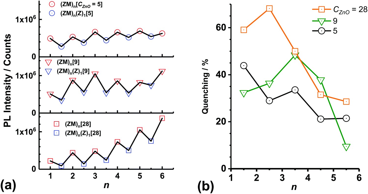 | ||
| Fig. 6 (a) PL intensity measured at λmaxversus bilayer number for the three ZnO NC/MDMO-PPV multilayer films. (b) Variation of the calculated quenching efficiency (Q) for the (ZM)n(Z)1 multilayer films. Values for Q were calculated from the data shown in (a) and eqn (4). | ||
The quenching efficiency (Q) for the multilayer films was calculated using the PL intensities shown in Fig. 6(a) and the following equation
 | (4) |
Solar cells fabricated using ZnO NC/MDMO-PPV multilayer films
Solar cells were constructed using the ZnO NC/MDMO-PPV multilayer films as the light harvesting component. It is understood that the use of one type of stacked acceptor/donor bilayer (or heterojunction) within a solar cell does not meet the energy level cascade requirements usually employed for high efficiency semiconducting NC/polymer solar cells.2,21,43 The aim of fabricating devices containing multilayer films (Fig. 7(a)) was to probe vertical transport of photo-generated charges. Devices were expected to fail through negligible short-circuit current densities (Jsc) if vertical charge transport was prevented. Representative J–V curves measured for the devices are shown in Fig. 7(b). The measured figures of merit appear in Fig. 7(c) and Table S1 (ESI†). A control bilayer device ((ZM)1) was also prepared. The MDMO-PPV layer thickness for that device (51 nm) was approximately eight times that of the MDMO-PPV layer thicknesses in the multilayer films. This relatively thick MDMO-PPV layer was required to achieve sufficient light absorption. The bilayer device PCE was 0.065 ± 0.019% which is close to the value of 0.08% reported for a ZnO NC/P3HT bilayer solar cell.44 | ||
| Fig. 7 (a) Depiction of fabricated device geometries showing the differences of the ZnO NC layer thicknesses. The (ZM)6 devices prepared using CZnO = 28.0 mg mL−1 did not provide reliable performance data. The ITO, PEDOT:PSS and Au layers are not drawn to scale. (b) Representative J–V curves for the (ZM)6 devices and a control (ZM)1 bilayer device. A (ZM)3 device was also prepared using CZnO = 14.0 mg mL−1 (see text). The CZnO values (mg mL−1) are shown in the legend. (c) Measured figures of merit plotted as a function of CZnO. | ||
The PCE values for the (ZM)6 devices were low compared to bulk heterojunction NC/polymer solar cells21,29 due to the much lower Jsc values for the present devices. A relatively low Jsc value is consistent with the limited area of the ZnO NC/MDMO-PPV interface in a planar film. It can be seen from the data shown in Fig. 7(c) that the (ZM)6 devices prepared using CZnO = 9.0–18.0 mg mL−1 had figures of merit that were similar to those for the bilayer device. The average Voc value for the (ZM)6 devices prepared using CZnO = 14.0 mg mL−1 was 796 ± 11 mV which is significantly higher than that measured for the bilayer devices (686 ± 88 mV). Interestingly, the former Voc is one of the highest reported for ZnO/MDMO-PPV solar cells.43 The relatively good performance of the multilayer cells is attributed to vertical pathways for holes and electrons that penetrated the ZnO NC and MDMO-PPV layers, respectively. In contrast it was not possible to fabricate reliable solar cells containing multilayer films prepared using CZnO = 28.0 mg mL−1. The relatively thick ZnO NC layers for those multilayer films (layer thickness = 32 nm) most likely contained less MDMO-PPV based on the CA results (see Fig. 3(b)). Hence, those multilayer films had fewer and more tortuous vertical hole transport pathways that spanned the whole ZnO NC layer thickness.
(ZM)3 devices were prepared using CZnO = 14.0 mg mL−1 in order to assess the effect of the number of bilayers on performance. The data measured are shown in Fig. 7(b) and (c) as well as Table S1 (ESI†). The average PCE for the (ZM)3 devices was 0.025 ± 0.005% which is 37% of the value for (ZM)6. Closer examination of the data showed that the average Jsc and Voc values for the (ZM)3 devices were, respectively, 83% and 53% of the average values for the (ZM)6 devices prepared using CZnO = 14.0 mg mL−1. The decrease for Jsc was statistically significant (p < 0.01 from a Student's t-test) and is attributed to less light being absorbed by a (ZM)3 film in accordance with the data shown in Fig. 4(b) for comparable films. The decrease in Voc is primarily attributed to the decreased shunt resistance (Rsh) for the (ZM)3 devices. The average Rsh values for the (ZM)6 and (ZM)3 devices were measured as 12.8 ± 2.5 kΩ cm2 and 4.7 ± 1.6 kΩ cm2, respectively. A small Rsh decreases the current flowing through the solar cell and decreases Voc.45 We conclude that the (ZM)6 multilayer devices gave the best PCE because of the greater light absorption and a higher Rsh.
Proposed morphology of ZnO NC/MDMO-PPV multilayer films
We propose a model in Fig. 8 for the morphologies of the ZnO NC/MDMO-PPV multilayer films based on all the data. The proposed morphologies contain ZnO NC layers that equal ∼1, 2 and 8 NC monolayers when CZnO = 5.0, 9.0 and 28.0 mg mL−1. Each of the NC layers is separated by a MDMO-PPV layer which is similar to the diameter of a MDMO-PPV globule. The coverage of the MDMO-PPV layers by the ZnO NC layers increased with increasing CZnO and was effectively complete for the multilayer film prepared using CZnO = 28.0 mg mL−1. We propose that there were numerous vertical percolated charge transport pathways for holes and electrons through the ZnO NC and MDMO-PPV layers, respectively, of the multilayer films prepared using CZnO = 5.0 and 9.0 mg mL−1. In contrast the film prepared using CZnO = 28.0 mg mL−1 did not have significant MDMO-PPV connectivity because the ZnO NC layers were too thick. Thus, the hole transport pathway was very inefficient in that film. | ||
| Fig. 8 Depiction of the proposed morphologies for ZnO NC/MDMO-PPV multilayer films. The concentration of MDMO-PPV within the ZnO NC layers is considered to be negligible for the film prepared using CZnO = 28.0 mg mL−1. The coverage of the MDMO-PPV layers by the ZnO NC layers increased with increasing CZnO. There were vertical charge transport pathways for holes and electrons for the films prepared using CZnO = 5.0 and 9.0 mg mL−1. However, these pathways for holes were tortuous and less effective for the films prepared using CZnO = 28.0 mg mL−1. Only the MDMO-PPV and ZnO NC layers and components are drawn to scale. | ||
Conclusions
In this study we have investigated the morphologies and optoelectronic properties of sequentially spin-coated ZnO NC/MDMO-PPV multilayer films. The ZnO NC layers had the same average thicknesses as those deposited on ITO glass. In contrast the average thickness for the MDMO-PPV layers was less than that deposited on ITO, which was probably due to some removal of some of the polymer by CHCl3 used for ZnO NC layer deposition. The CA data provided evidence that the coverage of the MDMO-PPV layers by the ZnO NC layers increased as the CZnO increased. The coverage was complete when CZnO = 28.0 mg mL−1. Light absorption by the multilayer films increased linearly with the number of MDMO-PPV layers deposited. The film absorption coefficient was tuneable using either layer thickness or CZnO. The PL data showed an unexpected 5 nm red-shift of the PL maximum for MDMO-PPV. Substantial and reversible PL quenching also occurred. The J–V data showed that the (ZM)6 devices performed well compared to a conventional (ZM)1 bilayer device. The maximum Voc values obtained for the (ZM)6 device prepared using CZnO = 14.0 mg L−1 is amongst the highest reported for ZnO NC/MDMO-PPV solar cells. The highly tuneable light absorption as well as the vertical charge transport for the ZnO NC/MDMO-PPV multilayer films studied here should also apply to other types of QD/polymer multilayer films and devices.Conflicts of interest
There are no conflicts of interest to declare.Acknowledgements
The authors thank the staff in the EM Core Facility in the Faculty of Biology, Medicine and Health for their assistance, and the Wellcome Trust for equipment grant support to the EM Core Facility. We also gratefully acknowledge funding from the EPSRC (Grant K009710/1).References
- J. Yan and B. R. Saunders, RSC Adv., 2014, 4, 43286–43314 RSC.
- S. Ren, L.-Y. Chang, S.-K. Lim, J. Zhao, M. Smith, N. Zhao, V. Bulović, M. Bawendi and S. Gradečak, Nano Lett., 2011, 11, 3998–4002 CrossRef CAS PubMed.
- W. J. Beek, M. M. Wienk and R. A. Janssen, Adv. Funct. Mater., 2006, 8, 1112–1116 CrossRef.
- S. D. Oosterhout, M. M. Wienk, M. Al-Hashimi, M. Heeney and R. A. J. Janssen, J. Phys. Chem. C, 2011, 115, 18901–18908 CAS.
- H. J. Snaith, A. Stavrinadis, P. Docampo and A. A. R. Watt, Sol. Energy, 2011, 85, 1283–1290 CrossRef CAS.
- N. Tulsiram, C. Kerr and J. I. L. Chen, J. Phys. Chem. C, 2017, 121, 26987–26996 CAS.
- K. Prashanthan, T. Thivakarasarma, P. Ravirajan, M. Planells, N. Robertson and J. Nelson, J. Mater. Chem. C, 2017, 5, 11758–11762 RSC.
- M. Eyer, J. Frisch, S. Sadofev, N. Koch, E. J. W. List-Kratochvil and S. Blumstengel, J. Phys. Chem. C, 2017, 121, 21955–21961 CAS.
- M. T. Khan and A. Almohammedi, J. Appl. Phys., 2017, 122, 075502 CrossRef.
- S. Dayal, N. Kopidakis, D. C. Olson, D. S. Ginley and G. Rumbles, Nano Lett., 2010, 10, 239–242 CrossRef CAS PubMed.
- W. Chen, M. P. Nikiforov and S. B. Darling, Energy Environ. Sci., 2012, 5, 8045–8074 CAS.
- M. Wright and A. Uddin, Sol. Energy Mater. Sol. Cells, 2012, 107, 87–111 CrossRef CAS.
- U. Jabeen, T. Adhikari, S. M. Shah, D. Pathak and J.-M. Nunzi, Opt. Mater., 2017, 73, 754–762 CrossRef CAS.
- S. A. McDonald, G. Konstantatos, S. Zhang, P. W. Cyr, E. J. D. Klem, L. Levina and E. H. Sargent, Nat. Mater., 2005, 4, 138 CrossRef CAS PubMed.
- G. Gou, G. Dai, X. Wang, Y. Chen, C. Qian, L. Kong, J. Sun and J. Yang, Appl. Phys. A: Mater. Sci. Process., 2017, 123, 731 CrossRef.
- X. Dai, Z. Zhang, Y. Jin, Y. Niu, H. Cao, X. Liang, L. Chen, J. Wang and X. Peng, Nature, 2014, 515, 96 CrossRef CAS PubMed.
- S. D. Oosterhout, M. M. Wienk, S. S. van Bavel, R. Thiedmann, L. Jan Anton Koster, J. Gilot, J. Loos, V. Schmidt and R. A. J. Janssen., Nat. Mater., 2009, 8, 818 CrossRef CAS PubMed.
- B. R. Saunders and M. L. Turner, Adv. Colloid Interface Sci., 2008, 138, 1–23 CrossRef CAS PubMed.
- S. D. Dimitrov and J. R. Durrant, Chem. Mater., 2014, 26, 616–630 CrossRef CAS.
- J. Zhao, Y. Li, G. Yang, K. Jiang, H. Lin, H. Ade, W. Ma and H. Yan, Nat. Energy, 2016, 1, 15027 CrossRef CAS.
- Z. Liu, Y. Sun, J. Yuan, H. Wei, X. Huang, L. Han, W. Wang, H. Wang and W. Ma, Adv. Mater., 2013, 25, 5772–5778 CrossRef CAS PubMed.
- E. A. Meulenkamp, J. Phys. Chem. B, 1998, 102, 5566–5572 CrossRef CAS.
- M. R. Waugh, G. Hyett and I. P. Parkin, Chem. Vap. Deposition, 2008, 14, 366–372 CrossRef CAS.
- R. M. Hewlett and M. A. McLachlan, Adv. Mater., 2016, 28, 3893–3921 CrossRef CAS PubMed.
- P. Zhang, J. Wu, T. Zhang, Y. Wang, D. Liu, H. Chen, L. Ji, C. Liu, W. Ahmad, Z. D. Chen and S. Li, Adv. Mater., 2018, 30, 1703737 CrossRef PubMed.
- P. Ravirajan, A. M. Peiro, M. K. Nazeeruddin, M. Graetzel, D. D. Bradley, J. R. Durrant and J. Nelson, J. Phys. Chem. B, 2006, 110, 7635–7639 CrossRef PubMed.
- J. Yan, Q. Lian, M. Z. Mokhtar, A. H. Milani, E. Whittaker, B. Hamilton, P. O’Brien, N. T. Nguyen and B. R. Saunders, Phys. Chem. Chem. Phys., 2017, 19, 27081–27089 RSC.
- G. P. Bartholomew and A. J. Heeger, Adv. Funct. Mater., 2005, 15, 677–682 CrossRef CAS.
- W. J. Beek, M. M. Wienk, M. Kemerink, X. Yang and R. A. Janssen, J. Phys. Chem. B, 2005, 109, 9505–9516 CrossRef CAS PubMed.
- S. B. Dkhil, D. Duché, M. Gaceur, A. K. Thakur, F. B. Aboura, L. Escoubas, J.-J. Simon, A. Guerrero, J. Bisquert, G. Garcia-Belmonte, Q. Bao, M. Fahlman, C. Videlot-Ackermann, O. Margeat and J. Ackermann, Adv. Energy Mater., 2014, 4, 1400805 CrossRef.
- H. L. Gao, X. W. Zhang, J. H. Meng, Z. G. Yin, L. Q. Zhang, J. L. Wu and X. Liu, J. Mater. Chem. A, 2015, 3, 3719–3725 CAS.
- A. P. Wanninayake, B. C. Church and N. Abu-Zahra, AIMS Mater. Sci., 2016, 3, 927–937 CrossRef CAS.
- S. Woo, W. Hyun Kim, H. Kim, Y. Yi, H.-K. Lyu and Y. Kim, Adv. Energy Mater., 2014, 4, 1301692 CrossRef.
- J. You, C. C. Chen, L. Dou, S. Murase, H. S. Duan, S. A. Hawks, T. Xu, H. J. Son, L. Yu, G. Li and Y. Yang, Adv. Mater., 2012, 24, 5267–5272 CrossRef CAS PubMed.
- D. H. Everett, Basic Principles of Colloid Science, RSC, Cambridge, 1988 Search PubMed.
- C. W. T. Bulle-Lieuwma, W. J. H. van Gennip, J. K. J. van Duren, P. Jonkheijm, R. A. J. Janssen and J. W. Niemantsverdriet, Appl. Surf. Sci., 2003, 203-204, 547–550 CrossRef CAS.
- P. Cooreman, R. Thoelen, J. Manca, M. vandeVen, V. Vermeeren, L. Michiels, M. Ameloot and P. Wagner, Biosens. Bioelectron., 2005, 20, 2151–2156 CrossRef CAS PubMed.
- L.-T. Lee, T. Ube, H. Aoki and S. Ito, Polymer, 2011, 52, 5897–5903 CrossRef CAS.
- R.-D. Sun, A. Nakajima, A. Fujishima, T. Watanabe and K. Hashimoto, J. Phys. Chem. B, 2001, 105, 1984–1990 CrossRef CAS.
- S. Wu, Q. Tai and F. Yan, J. Phys. Chem. C, 2010, 114, 6197–6200 CAS.
- R. C. Weast, CRC handbook of chemistry and physics, CRC Press, Florida, 65th edn, 1985 Search PubMed.
- D. Jarzab, M. Lu, H. T. Nicolai, P. W. M. Blom and M. A. Loi, Soft Matter, 2011, 7, 1702–1707 RSC.
- W. J. Beek, M. M. Wienk and R. A. J. Janssen, Adv. Mater., 2004, 16, 1009–1013 CrossRef CAS.
- S. R. Ferreira, R. J. Davis, Y.-j. Lee, P. Lu and J. W. P. Hsu, Org. Electron., 2011, 12, 1258–1263 CrossRef CAS.
- G. Jin, Z. Chen, C. Dong, Z. Cheng, X. Du, Q. Zeng, F. Liu, H. Sun, H. Zhang and B. Yang, ACS Appl. Mater. Interfaces, 2016, 8, 7101–7110 CAS.
Footnote |
| † Electronic supplementary information (ESI) available. See DOI: 10.1039/c8cp01148f |
| This journal is © the Owner Societies 2018 |