
 Open Access Article
 This Open Access Article is licensed under a
 Creative Commons Attribution 3.0 Unported Licence
Chemical-bond effect on epitaxial strain in perovskite sodium niobate†
L.
Yao
a,
S.
Inkinen
a,
O.
Pacherova
b,
M.
Jelinek
b,
S.
van Dijken
a and
M.
Tyunina
 *bc
*bc
aNanoSpin, Department of Applied Physics, Aalto University School of Science, P. O. Box 15100, FI-00076 Aalto, Finland
bInstitute of Physics of the Czech Academy of Sciences, Na Slovance 2, 18221 Prague, Czech Republic
cMicroelectronics Research Unit, Faculty of Information Technology and Electrical Engineering, University of Oulu, P. O. Box 4500, FI-90014, Finland. E-mail: marina.tjunina@oulu.fi
First published on 11th January 2018
Abstract
Epitaxial films and heterostructures of perovskite oxides attract tremendous scientific interest because of the unique phenomena therein. Especially important is the epitaxial growth of films subjected to substrate-induced misfit strain. We show here that in contrast to conventional misfit-controlled epitaxy, chemical bonds determine the crystal stability and strain in epitaxial films of sodium niobate on different cubic substrates. Strain relaxation in sodium niobate is independent of misfit magnitude and proceeds through perovskite-specific tilting of oxygen octahedra in addition to common defect formation. The observed structural relaxation evidences a major role of a large internal strain that originates from chemical bonds in the perovskite cell. The effect of chemical bonds on film strain is anticipated to also control the epitaxy of other perovskite oxides and related compounds.
Introduction
Single-crystal epitaxial films and heterostructures of complex ABO3-type perovskite oxides attract immense academic and technological interest due to breakthrough discoveries of emerging phenomena therein and their potential for electronic, photonic, spintronic, and other innovations.1–3 Remarkable progress has been achieved in the preparation of such films and heterostructures on different research and industrial substrates. Substrate-induced misfit strain significantly affects the material response, for instance: an increase or the appearance of ferroelectric polarization; tuning of structural, ferroic, and electronic phase transitions; emergence of multiferroic and magnetoelectric behaviour; ferromagnetic ordering; and other effects can be caused by strain.1–7 Correspondingly, much experimental effort is devoted to the synthesis of strained epitaxial films.4–7As is known from the well-established epitaxy of metals and common semiconductors, the elastic energy of any strained film increases up to a critical thickness, at which pseudomorphic growth terminates and the relaxation of misfit strain starts.8,9 The main mechanism for strain relaxation is through the formation of defects, such as dislocations, leading to a nearly quadratic dependence of the critical thickness d0 on the inverse magnitude of the misfit strain s: d0 ∝ s−2. The formation of defects is followed by columnar growth in thicker films. Epitaxy of perovskite oxides has also been found to obey these general trends, resulting in thickness dependent strain and properties.1–7,10–13 However, in contrast to simple metals and conventional semiconductors, the complex composition of ABO3 perovskites poses additional chemical conditions on crystal stability. A general perovskite cell consists of corner-shared BO6 octahedra surrounded by A-cations [Fig. 1(a–c)]. The B–O bond determines the lattice parameter aB of an ideal BO6-based cubic cell: aB = 2(rB + rO), where rB and rO are the radii of B- and oxygen ions, correspondingly.14 The phase stability of a BO6-based perovskite is restricted by the A–O bond, which defines a lattice parameter aA = √2(rA + rO).14 Depending on the radii of A-cations (rA), the BO6-octahedra can either experience a compressive (aB > aA) or tensile (aB < aA) strain [Fig. 1(d and e)]. The presence of chemical-bond-induced internal strain is typical for perovskites. In bulk unstressed perovskites, the BO6-octahedra can deform and tilt to release internal strain, thus leading to tetragonal, orthorhombic, rhombohedral, or hexagonal cells instead of an ideal cubic structure. The perovskite crystal phase is stable for the ratio 0.7 < (aA/aB) < 1.1.15 When a perovskite film grows pseudomorphically on top of a cubic substrate with the lattice parameter as, the BO6 octahedron should adjust itself to the substrate (aB = as) [Fig. 1(f)], which may improve or worsen the chemical internal stability of the perovskite.
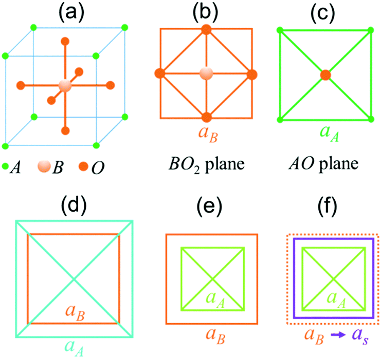 | ||
| Fig. 1 Schematics of ABO3 perovskite: (a) cubic cell, (b) BO2 plane and (c) AO-plane in an ideal cubic cell; internal (d) tensile strain (aB < aA) and (e) compressive strain (aB < aA) imposed on BO6 octahedra by A–O bonds; (f) effect of substrate in pseudomorphic epitaxial film. | ||
The chemical-bond-defined perovskite stability, internal strain, and perovskite-specific mechanisms of strain relaxation are often neglected in the analysis of epitaxial strain and strain relaxation as a function of perovskite film thickness. Although neglecting internal strain is justified for many films with aA/aB ≈ 1, the formation of specific defects and non-perovskite phases in other films point to the possible influence of chemical bonds on perovskite epitaxy.16–19
Here, we show that chemical bonds, which determine the stability of the perovskite phase, control epitaxial strain and its relaxation in perovskite sodium niobate (NaNbO3, or NNO) films. The renewed scientific interest in NNO is stimulated by the promising piezoelectric properties of technologically important lead-free solid solutions of KNbO3 and NNO.20–23 We experimentally investigate NNO films on two cubic substrates to ensure different misfit strains. We find a critical thickness that is independent of lattice mismatch. In addition to conventional defect and column formation, we observe vertical lamellar nanodomains, perovskite-structure supercells, and the evolution of NbO6-octahedral tilts across the film thickness. The detected structural relaxation evidences a major role of large internal strain, which originates from the chemical Nb–O and Na–O bonds in the perovskite cell of NNO.
Experimental
Epitaxial perovskite NNO films with a thickness of ∼150 nm and ∼10 nm and multilayers of alternating NNO and SrTiO3 (STO) nanofilms were grown by pulsed laser deposition. Single-crystal epitaxially polished (001) STO and (La0.18Sr0.82)(Al0.59Ta0.41)O3 (LSAT) substrates were used (MTI Corp.). The films were deposited at a temperature of 973 K and an oxygen pressure of 20 Pa. Post-deposition cooling was performed in an oxygen atmosphere. During this procedure, the oxygen pressure was gradually increased to 105 Pa.The crystal structure of the films was inspected by high-resolution X-ray diffraction (XRD) on a Bruker D8 DISCOVER diffractometer using Cu Kα radiation from a rotating anode tube. θ–2θ scans and reciprocal space maps were recorded and the in-plane and out-of-plane lattice parameters were determined from the positions of diffraction peaks using LEPTOS software and taking the substrates as the reference.
The microstructure of the films was investigated using transmission electron microscopy (TEM). The samples for cross-sectional TEM were prepared by standard mechanical polishing techniques. The analyses were carried out on a JEOL 2200FS TEM with double Cs correctors, operated at 200 kV. High-resolution TEM (HRTEM) imaging, scanning TEM imaging (STEM) with high-angle annular dark-field (HAADF) detector, selected area electron diffraction (SAED), and fast Fourier transform techniques (FFT) were applied. In HRTEM analysis, atomic-scale negative Cs imaging (NCSI) enabling the detection of atomic columns of oxygen24 was employed to analyze the tilting of oxygen octahedra.
Results and discussion
The commonly reported room-temperature phase of bulk unstressed NNO has an orthorhombic unit cell25–33 (space group Pbcm, with the lattice parameters a = 0.551 nm, b = 0.557 nm, and c = 1.552 nm), where three independent octahedral tilts lead to a √2ap × √2ap × 4ap supercell of the basic cubic perovskite subcell.30 Here, ap is the idealized cubic perovskite lattice parameter. Because clamping of pseudomorphic epitaxial films by cubic substrates suppresses tilts in such cube-on-cube-type films, the substrate-induced theoretical biaxial in-plane misfit strain in perovskite NNO is defined as sa = (as/aNNO − 1), where as is the substrate's lattice parameter and aNNO is the perovskite lattice parameter of NNO: aNNO ≈ 0.390 nm at room temperature and aNNO ≈ 0.394 nm at the deposition temperature. The estimated strain sa is approximately −0.35% on STO and −1.30% on LSAT during growth, and it decreases to 0% on STO and −0.9% on LSAT during cooling to room temperature. Considering the minor influence of thermal expansion mismatch, the good NNO/STO lattice match, and moderate NNO/LSAT misfit, one may expect pseudomorphic epitaxial growth of NNO on both substrates.The XRD analyses of the 10 nm-thick and 150 nm-thick NNO films show that the films grow with the (00l) planes parallel to the substrate surfaces and the [100] directions parallel to those in the substrates [Fig. S1, ESI†]. The crystal structure can be interpreted as metrically cubic with a lattice parameter of ∼0.390 nm in the 150 nm-thick films. The 10 nm-thick films possess metrically tetragonal cells with out-of-plane lattice parameters cf of ∼0.394 nm on STO and ∼0.393 nm on LSAT, while the in-plane parameters af are close to those of the substrates. The difference between the 150 nm-thick and 10 nm-thick films indicates an evolution of lattice strain across the film thickness and suggests full strain relaxation in the 150 nm-thick films. The observation of almost identical parameters cf in 10 nm-thick NNO films on different substrates points to possible strain relaxation therein. Therefore, the critical thickness may be smaller than 10 nm in NNO.
To get better insight into the crystal structure of the NNO films, the 150 nm-thick films were investigated by HRTEM [Fig. 2]. As can be seen in Fig. 2(a) and (c), vertical columns of tens of nanometers in width are present in the films. Despite the columnar microstructure, the films are epitaxial, as confirmed by electron diffraction [Fig. 2(b and d)]. The epitaxial relationship is (001)[100]film‖(001)[100]substrate, i.e., cube-on-cube-type for both substrates. Columnar microstructures that do not destroy epitaxy are often caused by the formation of dislocations and other defects and by subsequent three-dimensional island growth in strongly mismatched perovskite films. However, here, in addition to the defects [Fig. S2, ESI†] and columns, we detect peculiar lamellar nanodomains with a width of only 5–6 unit cells within the columns [Fig. 2(e and f)]. Incommensurate perovskite structural modulations like these have been observed before.34–36 It is known that oxygen octahedral tilts play a major role in the formation of such nanodomains. In NNO, NbO6-octahedral tilts are present in all low-temperature phases25–33 and incommensurate phases have also been found in bulk samples.29,37 The presence of fine nanodomains may therefore indicate local variations of tilting throughout the NNO films.
 | ||
| Fig. 2 Cross-sectional TEM analysis of 150 nm-thick NNO films. (a and c) STEM-HAADF images along the [010]p,s zone-axis illustrating a columnar microstructure. (b and d) SAED patterns of the NNO films on (b) STO and (d) LSAT. (e and f) HRTEM images and FFT patterns (insets) in the upper parts of the films. Lamellar nanodomains within the columns and FFT modulations around the main reflections indicate tilting variations. | ||
HRTEM images of the 25 nm-thick regions adjacent to the film–substrate interface show perfect in-plane coherency between the NNO films and the substrates, suggesting pseudomorphic growth [Fig. 3(a and d)]. However, fast Fourier transform (FFT) analysis reveals an evolution of the crystal structure within these regions [Fig. 3(b, c, e and f)]. In-plane four-fold symmetry, implying a tetragonal-type perovskite cell, is observed only in the first 5 nm of the film [Fig. 3(c and f)]. Beyond this, additional {1/2, 0, 1/2}p, {0, 1/2, 1/2}p, and {1/2, 1/2, 1/2}p reflections emerge in the FFT patterns [Fig. 3(b and e)]. These reflections indicate the presence of a [2 × 2 × 2] supercell built of perovskite subcells. Such a structural evolution can be caused by tilting of NbO6 oxygen octahedra, resembling the behavior in bulk NNO.25–33
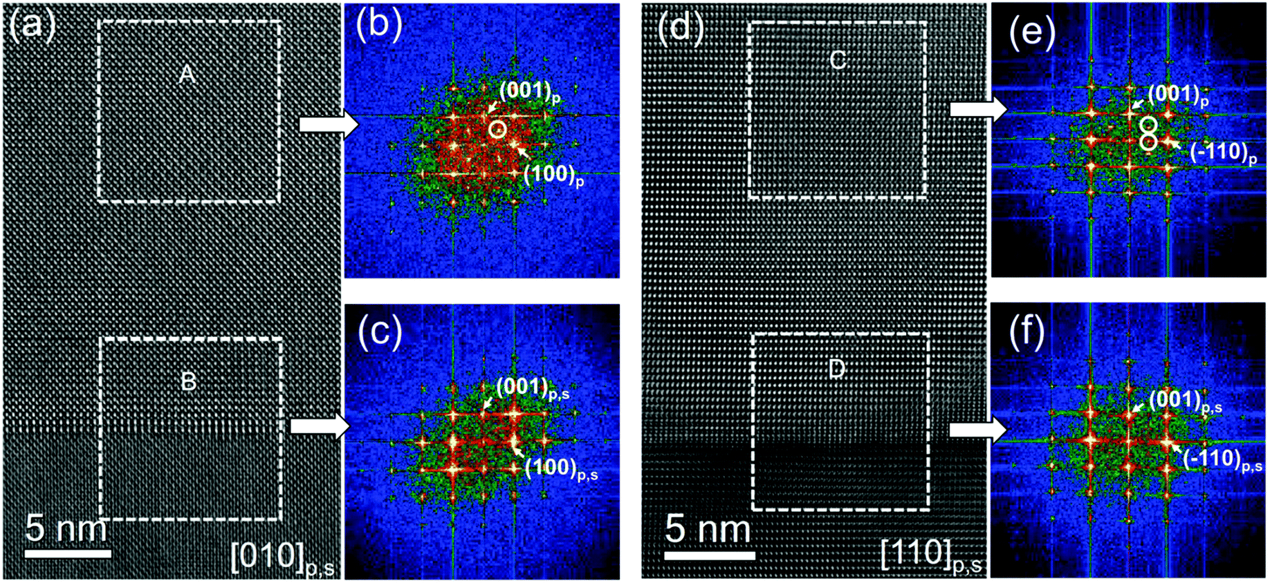 | ||
| Fig. 3 (a and d) Cross-sectional HRTEM images of NNO/STO along the (a) [010]p,s and (b) [110]p,s zone axes. (b, c, e and f) Selected area FFT patterns. The white circles mark extra reflections {1/2,0,1/2}p, {0,1/2,1/2}p and {1/2,1/2,1/2}p emerging in the [010]p and/or [110]p FFT patterns in the strain-relaxed regions (A and C), indicating the presence of a [2 × 2 × 2] supercell. | ||
To corroborate the presence of the oxygen octahedral tilts, we apply atomic-scale negative Cs imaging (NCSI) enabling detection of atomic columns of oxygen.24 HRTEM images of the NNO film and STO substrate acquired in NCSI mode (Cs = −30 μm) along the [110] zone axes are presented in Fig. 4(a–c). The atomic columns of oxygen are clearly distinguished and separated from the columns of Ti in STO and Nb in NNO. The octahedral tilt angles are determined from the coordinates of the atomic columns in the two-dimensional NSCI phase images. The obtained tilt angles are displayed in the maps in Fig. 4(d–f). Oxygen octahedral tilts are practically absent in the substrate [Fig. 4(d)], but start to emerge in the NNO film. The tilt angles are small at a distance of ∼4 nm from the interface [Fig. 4(e)]. However, at a distance of 10 nm, the tilt angles are significantly larger [Fig. 4(f)]. The results in Fig. 4 are consistent with the observations of fine nanodomains [Fig. 2(e and f)] and supercell reflections [Fig. 3(b and e)] and confirm the presence of oxygen octahedral tilts in the NNO films above a distance of 4 nm from the film–substrate interface. We note that defects start to form at the same distance [Fig. S2, ESI†].
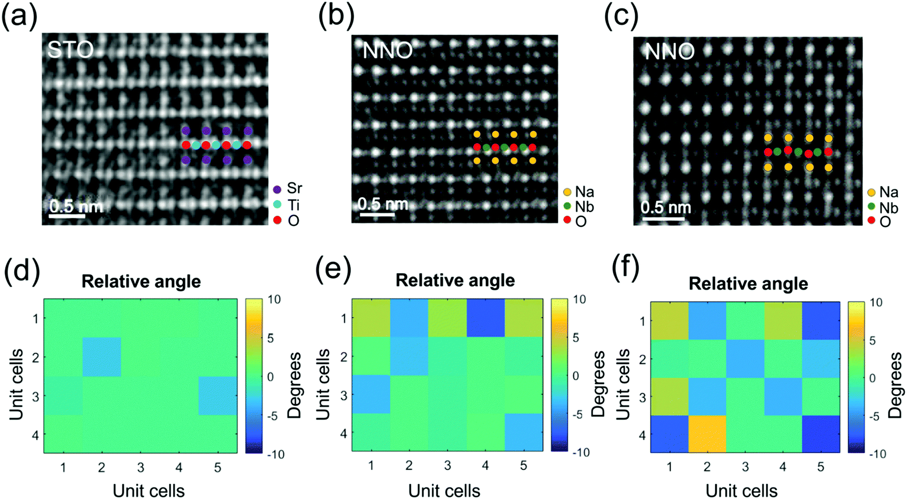 | ||
| Fig. 4 (a–c) HRTEM NCSI images along the [110]p,s zone axes and (d–f) maps of the oxygen octahedral tilt angles in the (a and d) STO substrate, (b and e) NNO film 4 nm from the interface, and (c and f) NNO film 10 nm from the interface. The Na, Nb, Sr, and Ti cations and O anions are marked by colored dots. | ||
Our experimental observations demonstrate that the NNO films grow pseudomorphically as tetragonal-type perovskites up to a thickness of approximately 4–5 nm both on the STO and LSAT substrates. Above this film thickness, NbO6-octahedral tilts emerge and defects appear. Further away from the film–substrate interface, the tilts manifest themselves in fine nanodomains within the columns, which, in turn, result from the formation of defects and a three-dimensional island growth mode. Thus, the critical thickness is relatively small, similar for different misfit strains, and connected to tilting of NbO6 octahedra.
To eliminate technological aspects in our study, we discuss multilayer stacks with a total thickness of ∼100 nm, built of alternating thin STO and NNO layers. In contrast to a separate uncapped film, elastic and electrostatic correlations between all layers stabilize epitaxy of multilayers.38 The STO:NNO epitaxial superlattices were grown on both STO and LSAT substrates. For an NNO thickness of ∼8 nm we find that the NNO layers are free of columns and lamellar nanodomains on both substrates [Fig. 5]. The emergence of defects and tilts in uncapped NNO films on STO or LSAT is thus not caused by imperfect growth conditions, but rather by strain relaxation therein.
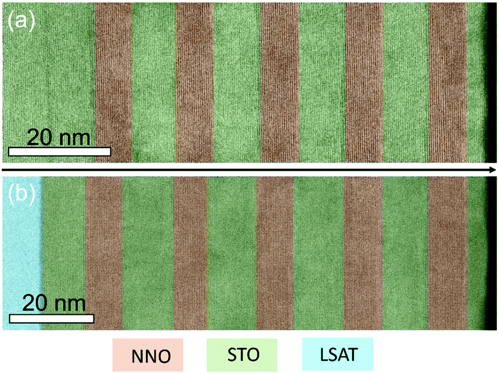 | ||
| Fig. 5 Cross-sectional STEM-HAADF images of NNO:STO superlattices on (a) STO and (b) LSAT substrates. The arrow indicates the direction from the substrate (left) to the top of the superlattice (right). | ||
Epitaxial strain relaxation in NNO clearly differs from the conventional relaxation of misfit strain through the formation of dislocations.8–10 We suggest that the chemical Na–O and Nb–O bonds are responsible for this peculiar behavior. The perovskite NNO unit cell consists of NbO6 octahedra surrounded by corner-shared Na cations. Compared to the lattice parameter aNb of an ideal NbO6-based cubic cell, the lattice parameter aNa of a NaO cube would be smaller.14,39 Consequently, NbO6-octahedra are compressed in bulk NNO. The magnitude of this three-dimensional internal strain can be estimated using Goldschmidt's lattice parameters and Shannon's ionic radii.14,39 For NNO, this strain is sNNO ≈ −3.3%. In bulk unstressed NNO, NbO6 octahedra deform and tilt to relax the internal strain sNNO. When the NbO6 octahedra are stressed in two of the three dimensions by a lattice mismatch with the underlying substrate, the parameter aNb changes and so does the internal strain sNNO. The resulting room-temperature total strain is roughly estimated as sNNO ≈ −3% in NNO/STO and sNNO ≈ −2% in NNO/LSAT. We note that because of the crystal chemistry, the total strain experienced by NNO is not equivalent to the misfit strain. Moreover, the total strain is reduced by the compressive misfit strain in the NNO/LSAT film. In contrast, the total strain increases under tensile misfit strain, making it difficult to achieve pseudomorphic growth.40,41
Relaxation of the total strain across the film thickness involves conventional and NNO-specific routes. Because the lattices of the NNO films are clamped by the cubic substrates, the relaxation of the total strain by tilting is suppressed at the interfaces.42 Consequently, the perovskite cell elongates in the out-of-plane direction. As revealed by XRD, the elongation is somewhat larger in the 10 nm-thick NNO/STO film than in the 10 nm-thick NNO/LSAT film, which is consistent with the larger total strain in the film on STO. The large magnitude of the total strain explains the small critical thickness of NNO films on both STO and LSAT. The concurrent emergence of tilts and defects at distances >4 nm from the interface evidences the coexistence of two strain relaxation routes: by NNO-specific tilting of oxygen octahedra and by conventional defect formation. Because the total strain differs from the misfit strain and the two relaxation routes coexist, the critical thickness does not obey the quadratic dependence on the inverse magnitude of the misfit strain. The 150 nm-thick NNO films are fully relaxed and contain random nanoregions with different tilting patterns. Because of the randomness and small size of these regions, the laboratory XRD shows a cubic structure on average.
Conclusions
In summary, our investigation of structural relaxation in epitaxial cube-on-cube-type perovskite NNO films reveals a small, misfit independent, critical thickness and the concurrent emergence of NbO6 octahedral tilts and defects. We find that a large internal strain, originating from chemical Nb–O and Na–O bonds, is responsible for this behavior. Because chemical-bond-induced internal strain exists in many perovskite-type oxides and other complex compounds, the crystal chemistry may also control epitaxial strain relaxation in these materials. The results of our work imply that an appropriate chemical design (e.g., via doping) may enable pseudomorphic epitaxial growth of rather thick perovskite films on mismatched substrates if the misfit strain is compensated by chemical-bond-induced internal strain.Conflicts of interest
There are no conflicts to declare.Acknowledgements
The authors acknowledge support from the Academy of Finland (Grant No. 293929 and 304291), the European Research Council (ERC-2012-StG 307502), the Grant Agency of the Czech Republic (Grant No. 15-15123S) and Infotech Oulu of the University of Oulu. TEM analysis was conducted at the Aalto University OtaNano – Nanomicroscopy Center (Aalto-NMC).References
- Epitaxial Growth of Complex Metal Oxides, ed. G. Koster, M. Huijben and G. Rijnders, Woodhead Publishing, Cambridge, 2015 Search PubMed.
- Multifunctional Oxide Heterostructures, ed. E. Y. Tsymbal, E. R. A. Dagotto, C.-B. Eom and R. Ramesh, Oxford University Press, Oxford, 2012 Search PubMed.
- M. Lorenz, et al. , J. Phys. D: Appl. Phys., 2016, 49, 433001 CrossRef.
- D. G. Schlom, L. Q. Chen, C. B. Eom, K. Rabe, S. K. Streiffer and J. M. Triscone, Annu. Rev. Mater. Res., 2007, 37, 589 CrossRef CAS.
- D. G. Schlom, L. Q. Chen, C. J. Fennie, V. Gopalan, D. A. Muller, X. Pan, R. Ramesh and R. Uecker, MRS Bull., 2014, 39, 118 CrossRef CAS.
- J. Li, Z. Shan and E. Ma, MRS Bull., 2014, 39, 108 CrossRef CAS.
- Y. Wang, H. Zhao, L. Zhang, J. Chen and X. Xing, Phys. Chem. Chem. Phys., 2017, 19, 17493 RSC.
- M. Ohring, The Materials Science of Thin Films, Academic Press, San Diego, 1992 Search PubMed.
- U. W. Pohl, Epitaxy of Semiconductors: Introduction to Physical Principles, Springer Verlag, Berlin Heidelberg, 2013 Search PubMed.
- J. S. Speck and W. Pompe, J. Appl. Phys., 1994, 76, 466 CrossRef CAS.
- I. Vrejoiu, G. Le Rhun, L. Pintilie, D. Hesse, M. Alexe and U. Gösele, Adv. Mater., 2006, 18, 1657 CrossRef CAS.
- R. J. Zeches, et al. , Science, 2009, 326, 977 CrossRef CAS PubMed.
- M. Tyunina, J. Narkilahti, M. Plekh, R. Oja, R. M. Nieminen, A. Dejneka and V. Trepakov, Phys. Rev. Lett., 2010, 104, 227601 CrossRef CAS PubMed.
- V. M. Goldschmidt, Die Naturwissenschaften, 1926, 14, 477 CrossRef CAS.
- H. Zhang, N. Li, K. Li and D. Xue, Acta Crystallogr., Sect. B: Struct. Sci., 2007, 63, 812 CAS.
- L. Lopez-Conesa, J. M. Rebled, D. Pesquera, N. Dix, F. Sanchez, G. Herranz, J. Fontcuberta, C. Magen, M. J. Casanove, S. Estrade and F. Peiro, Phys. Chem. Chem. Phys., 2017, 19, 9137 RSC.
- J. Xi, H. Xu, Y. Zhang and W. J. Weber, Phys. Chem. Chem. Phys., 2017, 19, 6264 RSC.
- M. D. Scafetta and S. J. May, Phys. Chem. Chem. Phys., 2017, 19, 10371 RSC.
- J. Li, D. Yin, Q. Li, R. Sun, S. Huang and F. Meng, Phys. Chem. Chem. Phys., 2017, 19, 6945 RSC.
- Y. Saito, H. Takao, T. Tani, T. Nonoyama, K. Takatori, T. Homma, T. Nagaya and M. Nakamura, Nature, 2004, 432, 84 CrossRef CAS PubMed.
- J. Wu, D. Xiao and Ji. Zhu, Chem. Rev., 2015, 115, 2559 CrossRef CAS PubMed.
- K. Xu, J. Li, X. Lv, J. Wu, X. Zhang, D. Xiao and J. Zhu, Adv. Mater., 2016, 28, 8519 CrossRef CAS PubMed.
- T. Zheng, H. Wu, Y. Yuan, X. Lv, Q. Li, T. Men, C. Zhao, D. Xiao, J. Wu, K. Wang, J.-F. Li, Y. Gu, J. Zhua and S. J. Pennycook, Energy Environ. Sci., 2017, 10, 528 CAS.
- C. L. Jia, M. Lentzen and K. Urban, Science, 2003, 299, 870 CrossRef CAS PubMed.
- S. K. Mishra, R. Mittal, V. Yu. Pomjakushin and S. L. Chaplot, Phys. Rev. B: Condens. Matter Mater. Phys., 2011, 83, 134105 CrossRef.
- I. Lefkowitz, K. Lukaszewicz and H. D. Megaw, Acta Crystallogr., 1966, 20, 670 CrossRef CAS.
- H. D. Megaw, Ferroelectrics, 1974, 7, 87 CrossRef CAS.
- C. N. W. Darlington and K. S. Knight, Acta Crystallogr., Sect. B: Struct. Sci., 1999, 24, 55 Search PubMed.
- Yu. I. Yuzyuk, et al. , J. Phys.: Condens. Matter, 2005, 17, 4977 CrossRef CAS.
- K. E. Johnston, C. C. Tang, J. E. Parker, K. S. Knight, P. Lightfoot and S. E. Ashbrook, J. Am. Chem. Soc., 2010, 132, 8732 CrossRef CAS PubMed.
- K. E. Johnston, J. M. Griffin, R. I. Walton, D. M. Dawson, P. Lightfoot and S. E. Ashbrook, Phys. Chem. Chem. Phys., 2011, 13, 7565 RSC.
- S. K. Mishra, N. Choudhury, S. L. Chaplot, P. S. R. Krishna and R. Mittal, Phys. Rev. B: Condens. Matter Mater. Phys., 2007, 76, 024110 CrossRef.
- M. D. Pee, S. P. Thompson, A. Daoud-Aladin, S. E. Ashbrook and P. Lightfoot, Inorg. Chem., 2012, 51, 687 Search PubMed.
- B. S. Guiton and P. K. Davies, Nat. Mater., 2007, 6, 586 CrossRef CAS PubMed.
- A. M. Abakumov, R. Erni, A. A. Tsirlin, M. D. Rossell, D. Batuk, G. Nénert and G. Van Tendeloo, Chem. Mater., 2013, 25, 2670 CrossRef CAS.
- S. García-Martín, G. King, G. Nénert, C. Ritter and P. M. Woodward, Inorg. Chem., 2012, 51, 4007 CrossRef PubMed.
- M. Tyunina, A. Dejneka, D. Rytz, I. Gregora, F. Borodavka, M. Vondracek and J. Honolka, J. Phys.: Condens. Matter, 2014, 26, 125901 CrossRef CAS PubMed.
- H. N. Lee, H. M. Christen, M. F. Chisholm, C. M. Rouleau and D. H. Lowndes, Nature, 2005, 433, 395 CrossRef CAS PubMed.
- R. D. Shannon, Acta Crystallogr., Sect. A: Cryst. Phys., Diffr., Theor. Gen. Crystallogr., 1976, 32, 751 CrossRef.
- J. Schwarzkopf, M. Schmidbauer, T. Remmele, A. Duk, A. Kwasniewski, S. B. Anooz, A. Devi and R. Fornari, J. Appl. Crystallogr., 2012, 45, 1015 CrossRef CAS.
- A. Duk, M. Schmidbauer and J. Schwarzkopf, Appl. Phys. Lett., 2013, 102, 091903 CrossRef.
- D. Kan, R. Aso, H. Kurata and Y. Shimakawa, APL Mater., 2015, 3, 062302 CrossRef.
Footnote |
| † Electronic supplementary information (ESI) available. See DOI: 10.1039/c7cp08449h |
| This journal is © the Owner Societies 2018 |