
A hybrid functional study of native point defects in Cu2SnS3: implications for reducing carrier recombination
Pin-Wen
Guan
 * and
Zi-Kui
Liu
* and
Zi-Kui
Liu
Department of Materials Science and Engineering, The Pennsylvania State University, University Park, Pennsylvania 16802, USA. E-mail: pxg928@psu.edu
First published on 10th November 2017
Abstract
The native point defects in the earth-abundant solar material Cu2SnS3 are studied using the hybrid functional. To generate more accurate formation energies of defects, the extended Freysoldt, Neugebauer, and Van de Walle (FNV) method is used for finite-size corrections in the charged supercell calculations. According to the calculated defect energetics, it is found that the usual experimental conditions can lead to abundant deep centers that deteriorate solar cell performance. To reduce the carrier recombination caused by the deep centers, Sn-rich and S-poor conditions should be attempted. The present calculations also give satisfactory explanations for a recent experimental work on the defect levels in Cu2SnS3.
1. Introduction
Recently, there has been increasing interest in searching for earth-abundant solar materials such as Cu2ZnSn(S,Se)4,1 ZnSnP2,2 and Cu2SnS3.3 Photovoltaic device efficiencies greater than 4% and 6% have been achieved based on Cu2SnS3 and its alloy, respectively.4–6 The bandgap of Cu2SnS3 is usually reported at approximately 0.9–1 eV,6–10 and can be tuned by alloying with Si or Ge on the Sn site.5,11 The conversion efficiency of Cu2SnS3 solar cells depends on many factors such as the p–n junction interface and properties of the Cu2SnS3 absorber including morphology, secondary phases, and point defects.12 While morphology and secondary phases have been relatively well controlled, the understanding and control of point defects are still insufficient for Cu2SnS3.12 Point defects are difficult to experimentally measure, and thus, theoretical calculations are important and valuable.13 There are some theoretical works regarding the defect chemistry of Cu2SnS3 in the literature,3,14 but only the functionals at the local density approximation (LDA)/generalized gradient approximation (GGA) level are used, and thus, their reliability is questionable. In addition, finite-size corrections are needed for charged defects, but the proper correction method has long been debated.Komsa et al.15 compared several major methods and found that the scheme proposed by Freysoldt, Neugebauer, and van de Walle (FNV)16 provides overall superior performance. Later, Kumagai et al. extended the FNV method to anisotropic systems by using the atomic site potential.17 It is noted that both the original FNV method and the extended method have been implemented in high-throughput defect calculations.18 The aim of the present work is to determine more accurate defect energetics of Cu2SnS3 by using hybrid functionals and the extended FNV method, which is important for controlling the point defects and the conversion efficiency of Cu2SnS3.
2. Computational details
All first-principles calculations in the present work are based on density functional theory (DFT),19,20 using the projector augmented wave (PAW)21 method implemented in the Vienna Ab initio Simulation Package (VASP).22,23 The (semi)local functionals such as LDA and GGA24 usually underestimate the bandgap and cannot correctly describe point defects; thus the Heyd–Scuseria–Ernzerhof (HSE) hybrid functional25 is used due to its improved performance with regard to these aspects. The HSE functional mixes 25% of screened Hartree–Fock exchange with the screening parameter being 0.2 Å−1, and is used in conjunction with PBEsol26 for a more accurate description of solids, as well as the D3 correction for the van der Waals force, which is important for correctly predicting thermochemical quantities in sulfur-bearing systems.27 This functional combination can be termed as HSEsol + D3.28For the defect calculations, a 2 × 1 × 2 supercell (constructed from the conventional unit cell) is used that consists of 96 atoms when the supercell is defect-free and a 2 × 2 × 2 mesh of Monkhorst–Pack k-points.29 An energy cutoff of 280 eV is used for plane-wave basis expansion in all the calculations, which is similar to the cutoff used in a hybrid functional study of point defects in Cu2ZnSnS4.30 A larger cutoff of 370 eV leads to changes below 5 meV per atom in the formation energies of compounds in the Cu–Sn–S system according to the test calculations, which are sufficiently small for the purposes of the present work. The residual forces after geometry optimization are less than 0.02 eV Å−1. For the finite-size corrections for charged-defect supercell calculations, the extended FNV method proposed by Freysoldt et al.16 and modified by Kumagai17 is used.
The formation energy of a point defect is calculated as2
 | (1) |
The thermodynamic transition level between the charge states q and q′ of the defect D referenced to the valence band maximum (VBM) is calculated as2
 | (2) |
Finite-size corrections are also needed for the defect single-particle levels. The following corrections2,15,31 are used:
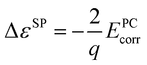 | (3) |
3. Results and discussion
3.1. Properties of the perfect crystal
Several structures of Cu2SnS3 have been previously reported, including cubic, tetragonal, monoclinic, and triclinic.5,32,33 All these structures are varieties of the zincblende structure with different degrees of Cu/Sn disorder. In the present work, only the monoclinic structure illustrated in Fig. 1 was studied for simplicity; it has 24 atoms in the conventional unit cell with the space group Cc. The calculated lattice parameters listed in Table 1 are in good agreement with the experimental values. The slightly smaller experimental lattice parameters may be partly caused by abundant thermal vacancies due to their low formation energies, which will be shown later. Because the dielectric constants are important in the finite-size corrections for charged defects, they were also calculated and are listed in Table 1. Due to the Cc symmetry, the dielectric tensor has four independent components, showing weak anisotropy. The total dielectric tensor εtot is the sum of the ion-clamped dielectric tensor εele and the ionic contribution εion. It can be seen that εion much less contributed to εtot than εele from Table 1, because the ionicity of Cu2SnS3 is not very strong. The band structure is plotted in Fig. 2, clearly showing that Cu2SnS3 is a direct bandgap semiconductor, with both VBM and conduction band minimum (CBM) located at the Γ point. The calculated bandgap is 0.80 eV, which is the same as the value obtained from another HSE study,34 and is also in reasonable agreement with the experimental values at approximately 0.9–1 eV.6–10 | ||
| Fig. 1 Crystal structure of the monoclinic Cu2SnS3. The Cu, Sn, and S atoms are represented by the red, grey, and yellow spheres, respectively. | ||
| Lattice parameter | ε ele | ε ion | ε tot | |
|---|---|---|---|---|
|
Cu2SnS3
Cc (#9) 24 atoms |
a = 6.601 Å | ε 11 = 10.16 | ε 11 = 3.71 | ε 11 = 13.87 |
| b = 11.425 Å | ε 22 = 10.86 | ε 22 = 3.69 | ε 22 = 14.55 | |
| c = 6.607 Å | ε 33 = 11.48 | ε 33 = 4.18 | ε 33 = 15.66 | |
| β = 109.44° | ε 13 = −1.61 | ε 13 = 0.38 | ε 13 = −1.23 | |
| Expt. | a = 6.449 Å | NA | NA | NA |
| b = 11.319 Å | ||||
| c = 6.428 Å | ||||
| β = 108.37° | ||||
 | ||
| Fig. 2 Band structure of the monoclinic Cu2SnS3. | ||
3.2. Chemical potential diagram
The stability of Cu2SnS3 is limited by the other phases in the Cu–Sn–S system. The formation energies of the compounds in the Cu–Sn–S system were calculated using HSEsol + D3 and are listed in Table 2. An overall agreement between the calculations and the experiments35–38 was found, although it is still difficult to achieve chemical accuracy (approximately 0.04 eV per atom) by DFT at the current stage even when using chemically similar references.39 For comparison, the results calculated by PBEsol + D3 are also listed in Table 2, showing poorer agreement with the experimental values than those calculated by HSEsol + D3. Using the formation energies calculated by HSEsol + D3, the chemical potential diagram of the Cu–Sn–S system is generated and visualized in Fig. 3. Cu2SnS3 is surrounded by Cu, Cu2S, Cu5Sn2S7, Cu4Sn7S16 and SnS, which are therefore the possible secondary phases in Cu2SnS3. Within the stable region of Cu2SnS3, the variation of Cu chemical potential is small, while both Sn and S have large variation in their chemical potential, which has an important consequence in the point defects, as will be discussed later. It should be noted that the phase equilibria is dependent on the temperature, which has been revealed by our previous work,40 although we focus on the 0 K first-principles calculations in the present work. It is also noted that Cu4SnS4 and Cu3SnS4 do not appear in the chemical potential diagram because they are not thermodynamically stable against other phases, according to the present calculations.![[3 with combining macron]](https://www.rsc.org/images/entities/char_0033_0304.gif) m), tetragonal Sn (I41/amd), and orthorhombic S (Fddd)
m), tetragonal Sn (I41/amd), and orthorhombic S (Fddd)
| Compound | Space group | E f | ||
|---|---|---|---|---|
| PBEsol + D3 | HSEsol + D3 | Expt. | ||
| Cu2S | P21/c | −0.45 | −0.76 | −0.8335 |
| CuS | P63/mmc | −0.45 | −0.54 | −0.5536 |
| SnS | Pnma | −1.00 | −0.99 | −1.1337 |
| SnS2 |
Pml |
−1.36 | −1.47 | −1.5737 |
| Cu2SnS3 | Cc | −2.21 | −2.80 | −2.5238 |
| Cu4SnS4 | Pnma | −2.46 | −3.51 | −3.4038 |
| Cu4Sn7S16 |
Rm |
−11.17 | −13.03 | NA |
| Cu3SnS4 |
I![[4 with combining macron]](https://www.rsc.org/images/entities/char_0034_0304.gif) 2m 2m |
−3.04 | −3.39 | NA |
| Cu5Sn2S7 | C2 | −5.34 | −6.29 | NA |
 | ||
| Fig. 3 Chemical potential diagram of the Cu–Sn–S system based on 0 K HSEsol + D3 calculations. | ||
3.3. Native point defects
The native point defects of Cu2SnS3 studied in the present work include VCu, VSn, VS, CuSn, and SnCu. The sulfur atoms have two different coordinations, consisting of “three Cu plus one Sn” and “two Cu plus two Sn,” respectively, therefore leading to two types of S vacancies, VS1 and VS2. The thermodynamic transition levels between different charge states of defects are listed in Table 3, including both the uncorrected values and the corrected ones. The extended FNV method employed here is not applicable to the defects with the perturbed host state (PHS), which is very delocalized and spills out from the supercell, making the correction method invalid.2,17 The defect with PHS has small thermal ionization energy, typically less than 0.1 eV.2 In Table 3, three uncorrected levels are close to the band edge, including VCu (0/−1), VSn (0/−1) and CuSn (0/−1), and are thus related to small thermal ionization energy and possibly PHS. The holes in V0Cu, V0Sn, and Cu0Sn are possible PHS. One method for determining if a defect level is PHS is based on its scaling behavior with the size of the supercell,15 which may be not efficient. Here, the squared wavefunction of the studied defect state41 is used for this purpose. Fig. 4 shows the squared wavefunction of the lowest unoccupied states of V0Cu, V0Sn, and Cu0Sn. It can be clearly seen that the hole in V0Cu is very delocalized and spills out from the supercell, while for V0Sn and Cu0Sn, the holes are relatively localized and contained in the supercell, despite a certain extent of delocalization. Therefore, it is justified to treat V0Sn and Cu0Sn in the framework of the extended FNV method, i.e., the correction is zero due to the zero charge, but this is not true for V0Cu due to its acceptor-like PHS. To address this issue, it is simply approximated that εth(VCu,0/−1) ≈ 0, as the treatment in the literature.2 After the corrections, the thermodynamic transition levels are deeper, and some of them are removed from the bandgap, with the remaining deep levels being VSn (0/−1), VSn (−1/−2), and CuSn (0/−1). Both VS1 and VS2 have no thermodynamic transition levels within the bandgap, regardless of whether the corrections are applied or not. A comparative example is the sulfur vacancy in Cu2ZnSnS4 (CZTS), which also has no transition levels in the bandgap.30 It is noted that a previous GGA level study reports the charge states within the bandgap ranging from [−1,0], [−4,0], [−3,0], and [0,3] for VCu, VSn, CuSn, and SnCu, respectively,3 which is similar to the present uncorrected results.| Defect | q/q′ | ε th (uncorrected) | ε th (corrected) |
|---|---|---|---|
| V Cu | 0/−1 | −0.067 | 0 |
| V Sn | 0/−1 | 0.093 | 0.470 |
| −1/−2 | 0.120 | 0.689 | |
| −2/−3 | 0.146 | >CBM | |
| −3/−4 | 0.382 | >CBM | |
| CuSn | 0/−1 | −0.049 | 0.241 |
| −1/−2 | 0.314 | >CBM | |
| −2/−3 | 0.384 | >CBM | |
| SnCu | +1/+2 | 0.121 | <VBM |
| +2/+3 | 0.541 | <VBM |
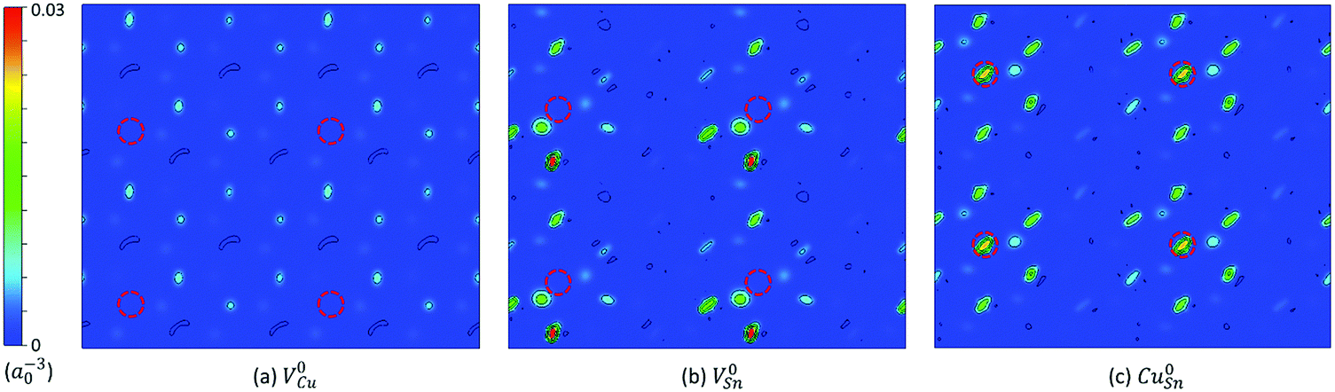 | ||
| Fig. 4 Squared wavefunction of the lowest unoccupied state of (a) neutral Cu vacancy V0Cu, (b) neutral Sn vacancy V0Sn, and (c) neutral antisite Cu0Sn within the (001) plane through the position of the defect in the monoclinic Cu2SnS3. The unit of the squared wavefunction is a0−3, where the Bohr radius a0 = 0.529 Å. The contour lines are spaced by 0.005 a0−3. Each figure contains four supercells. The position of the defect is indicated by the red dashed circle. | ||
The local structures and defect single-particle levels of selected defects are illustrated in Fig. 5. For VCu−1, the distances between the vacancy and the neighboring S atoms are 2.19–2.27 Å [Fig. 5(a)], while in the perfect crystal, the Cu atom forms three bonds of 2.28 Å and one bond of 2.33 Å with the neighboring S atoms. VCu−1 has no in-gap states [Fig. 5(a)]. As shown in Fig. 5(b) and (c), V0Sn and VSn−2 have rather different geometric and electronic structures. In the perfect crystal, the Sn atom forms two bonds of 2.36 Å and two bonds of 2.47 Å with the neighboring S atoms. For V0Sn, the distances between the vacancy and the neighboring S atoms are 2.21–2.31 Å, and there are two unoccupied defect single-particle levels slightly above VBM. For VSn−2, one S atom has a significantly larger distance of 2.35 Å with the vacancy, compared to the corresponding value of 2.25 Å for V0Sn. The two defect levels of VSn−2 are within the upper part of the bandgap, with the lower one fully occupied. From Fig. 5(d) and (e), it can be seen that CuSn−1 has two Cu–S bonds of 2.36 and 2.40 Å, larger than those of 2.33 and 2.36 Å in Cu0Sn, respectively. The two defect levels of Cu0Sn are within the lower part of the bandgap, with the lower one at VBM half occupied. CuSn−1 has only one in-gap defect level, which is in the upper part of the bandgap and unoccupied. SnCu+1 has Sn–S bonds of 2.61–2.73 Å, and has no in-gap states but has an occupied defect level 0.11 eV below VBM [Fig. 5(f)].
 | ||
| Fig. 5 Local structures and defect single-particle levels of selected point defects in the monoclinic Cu2SnS3. The position of a vacancy is defined as the geometric center of the neighboring atoms. The distances between the defect and its neighboring atoms are in units of Å. The corrected defect single-particle levels are labeled with their positions relative to VBM in eV. The defect single-particle levels located in the valence or conduction band before the correction are schematically represented by dashed lines, because they are not clearly defined. | ||
The formation energies of point defects in Cu2SnS3 are calculated under two different conditions of (μ(Cu), μ(Sn), μ(S)) represented by A = (−0.606, −1.303, −0.092) eV and B = (0, −0.081, −0.905) eV in Fig. 3, respectively. The secondary phases at A are Cu5Sn2S7 and Cu4Sn7S16, while those at B are Cu and SnS. The results are shown in Fig. 6. No matter under which condition, the most favorable charged defect is VCu−1, making Cu2SnS3 p-type the intrinsic type with the minority carriers being electrons. Under condition A, the pinning level of VCu−1, where its formation energy becomes zero, is far away from CBM, making n-type doping very difficult under this condition. CuSn and VSn are deep centers, which have defect levels deep in the bandgap and are detrimental for solar cell performance because they can accelerate electron–hole recombination. CuSn should be more abundant than VSn due to its lower formation energy. In the p-type conditions, i.e., when the Fermi level is near VBM, the formation energy of Cu0Sn is only approximately 0.94 eV, leading to a concentration of approximately 1016 cm−3 at a typical growth temperature of 550 °C. Such abundant Cu0Sn can effectively capture electrons, severely limiting the minority carrier life and reducing the conversion efficiency. Similarly, CuSn is also found in a deep center in Cu2ZnSnS4, but the formation energy is higher.30 Under condition B, VCu is less favorable compared with the situation under A, and no pinning level occurs within the bandgap, making n-type doping possible. The deep centers CuSn and VSn are also less favorable. At first glance, this seems slightly counterintuitive for CuSn, because B has such a high Cu chemical potential that Cu metals form. However, B also has the highest Sn chemical potential within the stable region of Cu2SnS3. Because Sn has much larger variation in its chemical potential than Cu, it plays a dominant role in the formation of CuSn. Therefore, it is seen that the phase stability has a profound influence on the defect chemistry.
 | ||
| Fig. 6 Formation energies of native point defects in the monoclinic Cu2SnS3 under condition (a) A and condition (b) B. The Fermi level is referenced to the VBM. | ||
In the experiments, usually S-rich conditions are employed, which are closer to condition A, resulting in abundant CuSn deep centers according to the present calculations. This may be one of the reasons why the conversion efficiency of pure Cu2SnS3 solar cells has not exceeded 5%4 thus far. Condition B can reduce CuSn and VSn, but the drawback is the existence of Cu, which may reduce the shunt resistivity and be detrimental for solar cell performance. It may be more optimal to slightly decrease the Cu chemical potential from B and enter into the single phase Cu2SnS3 region or the Cu2SnS3/SnS mixture region to avoid the formation of Cu while maintaining low concentrations of the CuSn deep center. This condition is relatively Sn-rich and S-poor. Admittedly, the solar cell performance is also determined by many factors in addition to the concentration of deep centers, although we are focusing on point defects here.
According to the present calculations, the two most abundant transition levels are εth(VCu,0/−1) ≈ 0 and εth(CuSn,0/−1) = 241 meV, while the other transition levels are associated with much higher formation energies and with more difficult detection. A recent experimental study found two trap levels with activation energies of 41 ± 0.4 meV and 206 ± 7 meV based on impedance spectroscopy,42 which are in excellent agreement with our results. The satisfactory explanation of experimental facts demonstrates the soundness of the methods used in the present study. It is worth noting that there are large discrepancies in previous theoretical works employing GGA level calculations.3,14 For instance, in ref. 3, the formation energy of Cu0Sn is above 2.5 eV, but in ref. 14, it is below 1 eV and can be even less than −0.5 eV under some conditions. Such discrepancies indicate that the GGA level calculations may not be sufficiently reliable, and additional sophisticated tools such as the hybrid functionals are necessary.
4. Conclusion
In the present work, the native point defects in the earth-abundant solar material Cu2SnS3 are studied using the hybrid functional and the extended FNV method for finite-size corrections in the supercell calculations. First, the properties of the perfect crystal are calculated and the stable region of Cu2SnS3 is determined based on the chemical potential diagram of the Cu–Sn–S system. Then, the thermodynamic transition levels of the studied defects are calculated and corrected based on the extended FNV method. Prior to performing the corrections, the neutral Cu vacancy is identified as the defect with the perturbed host state based on the squared wavefunction analysis, which cannot be addressed with the extended FNV method. The number of charge states within the bandgap is much less than that obtained in the previous study. Third, the local structures and defect single-particle levels are analyzed for selected defects. Fourth, the defect formation energies are calculated under different conditions, indicating that the typical experimental conditions may lead to a high concentration of deep centers that are detrimental for solar cell performance. The Sn-rich and S-poor condition is proposed to reduce deep centers. Last, it is found that the present calculations provide satisfactory explanations for a recent experimental work on defect levels. The present work provides useful insights into the defect chemistry of Cu2SnS3, which are indispensable for understanding and improving its properties.Conflicts of interest
There are no conflicts of interest to declare.Acknowledgements
This work was financially supported by the NSF with Grant No. CHE-1230924 and CHE-1230929. First-principles calculations were carried out on the LION clusters at Pennsylvania State University. Calculations were also carried out on the CyberStar cluster funded by the NSF through Grant No. OCI-0821527. The crystal structure and the squared wavefunction were plotted using VESTA.43 Visualization of the chemical potential diagram was performed with CHESTA.44References
- H. Katagiri, K. Jimbo, S. Yamada, T. Kamimura, W. S. Maw, T. Fukano, T. Ito and T. Motohiro, Appl. Phys. Express, 2008, 1, 0412011 CrossRef.
- Y. Kumagai, M. Choi, Y. Nose and F. Oba, Phys. Rev. B: Condens. Matter Mater. Phys., 2014, 90, 1–12 CrossRef.
- L. L. Baranowski, P. Zawadzki, S. Christensen, D. Nordlund, S. Lany, A. C. Tamboli, L. Gedvilas, D. S. Ginley, W. Tumas, E. S. Toberer and A. Zakutayev, Chem. Mater., 2014, 26, 4951–4959 CrossRef CAS.
- A. Kanai, K. Toyonaga, K. Chino, H. Katagiri and H. Araki, Jpn. J. Appl. Phys., 2015, 54, 08KC06 CrossRef.
- M. Umehara, Y. Takeda, T. Motohiro, T. Sakai, H. Awano and R. Maekawa, Appl. Phys. Express, 2013, 6, 045501 CrossRef.
- M. Nakashima, J. Fujimoto, T. Yamaguchi and M. Izaki, Appl. Phys. Express, 2015, 8, 042303 CrossRef.
- R. Chierchia, F. Pigna, M. Valentini, C. Malerba, E. Salza, P. Mangiapane, T. Polichetti and A. Mittiga, Phys. Status Solidi, 2016, 13, 35–39 CrossRef CAS.
- T. Nomura, T. Maeda and T. Wada, Jpn. J. Appl. Phys., 2014, 53, 05FW01 CrossRef.
- J. A. Marquez Prieto, S. Levcenko, J. Just, H. Hampel, I. Forbes, N. M. Pearsall and T. Unold, J. Alloys Compd., 2016, 689, 182–186 CrossRef CAS.
- A. Kanai, H. Araki, A. Takeuchi and H. Katagiri, Phys. Status Solidi, 2015, 252, 1239–1243 CrossRef CAS.
- K. Toyonaga and H. Araki, Phys. Status Solidi, 2015, 12, 753–756 CrossRef CAS.
- A. C. Lokhande, R. B. V. Chalapathy, M. He, E. Jo, M. Gang, S. A. Pawar, C. D. Lokhande and J. H. Kim, Sol. Energy Mater. Sol. Cells, 2016, 153, 84–107 CrossRef CAS.
- C. Freysoldt, B. Grabowski, T. Hickel, J. Neugebauer, G. Kresse, A. Janotti and C. G. Van de Walle, Rev. Mod. Phys., 2014, 86, 253 CrossRef.
- H. Nishihara, T. Maeda, A. Shigemi and T. Wada, Jpn. J. Appl. Phys., 2016, 55, 04ES08 CrossRef.
- H. P. Komsa, T. Rantala and A. Pasquarello, Phys. Rev. B: Condens. Matter Mater. Phys., 2012, 407, 3063–3067 CrossRef CAS.
- C. Freysoldt, J. Neugebauer and C. G. Van de Walle, Phys. Rev. Lett., 2009, 102, 16402 CrossRef PubMed.
- Y. Kumagai and F. Oba, Phys. Rev. B: Condens. Matter Mater. Phys., 2014, 89, 195205 CrossRef.
- D. Broberg, B. Medasani, N. Zimmermann, A. Canning, M. Haranczyk, M. Asta and G. Hautier, 2016, arXiv:1611.07481.
- P. Hohenberg and W. Kohn, Phys. Rev. B: Condens. Matter Mater. Phys., 1964, 136, B864 Search PubMed.
- W. Kohn and L. J. Sham, Phys. Rev., 1965, 140, A1133 CrossRef.
- P. E. Blochl, Phys. Rev. B: Condens. Matter Mater. Phys., 1994, 50, 17953–17979 CrossRef.
- G. Kresse and J. Furthmüller, Phys. Rev. B: Condens. Matter Mater. Phys., 1996, 54, 11169–11186 CrossRef CAS.
- G. Kresse and J. Furthmuller, Comput. Mater. Sci., 1996, 6, 15–50 CrossRef CAS.
- J. P. Perdew, K. Burke and M. Ernzerhof, Phys. Rev. Lett., 1996, 77, 3865–3868 CrossRef CAS PubMed.
- A. V. Krukau, O. A. Vydrov, A. F. Izmaylov and G. E. Scuseria, J. Chem. Phys., 2006, 125, 224106 CrossRef PubMed.
- J. P. Perdew, A. Ruzsinszky, G. I. Csonka, O. A. Vydrov, G. E. Scuseria, L. A. Constantin, X. L. Zhou and K. Burke, Phys. Rev. Lett., 2008, 100, 136406 CrossRef PubMed.
- P.-W. Guan, S.-L. Shang, G. Lindwall, T. Anderson and Z.-K. Liu, J. Alloys Compd., 2017, 694, 510–521 CrossRef CAS.
- L. Schimka, J. Harl and G. Kresse, J. Chem. Phys., 2011, 134, 024116 CrossRef PubMed.
- H. J. Monkhorst and J. D. Pack, Phys. Rev. B: Condens. Matter Mater. Phys., 1976, 13, 5188–5192 CrossRef.
- D. Han, Y. Y. Sun, J. Bang, Y. Y. Zhang, H. B. Sun, X. Bin Li and S. B. Zhang, Phys. Rev. B: Condens. Matter Mater. Phys., 2013, 87, 1–5 Search PubMed.
- W. Chen and A. Pasquarello, Phys. Rev. B: Condens. Matter Mater. Phys., 2013, 88, 115104 CrossRef.
- D. Avellaneda, M. T. S. Nair and P. K. Nair, J. Electrochem. Soc., 2010, 157, D346–D352 CrossRef CAS.
- K. Chino, J. Koike, S. Eguchi, H. Araki, R. Nakamura, K. Jimbo and H. Katagiri, Jpn. J. Appl. Phys., 2012, 51, 10NC35 CrossRef.
- L. Xi, Y. B. Zhang, X. Y. Shi, J. Yang, X. Shi, L. D. Chen, W. Zhang, J. H. Yang and D. J. Singh, Phys. Rev. B: Condens. Matter Mater. Phys., 2012, 86, 155201 CrossRef.
- K. C. Mills, Thermodynamic data for inorganic sulphides, selenides and tellurides, Butterworths, London, 1974 Search PubMed.
- F. Westrum, J. Chem. Thermodyn., 1987, 19, 1199 CrossRef.
- H. Gamsjäger, T. Gajda, J. Sangster, S. K. Saxena and W. Voigt, Chemical thermodynamics of tin, Nuclear Energy Agency, 2013 Search PubMed.
- M. B. Babanly, in Electromotive Force and Measurement in Several Systems, ed. S. Kara, Intechweb. Org., 2011, pp. 57–78 Search PubMed.
- A. Jain, G. Hautier, S. P. Ong, C. J. Moore, C. C. Fischer, K. A. Persson and G. Ceder, Phys. Rev. B: Condens. Matter Mater. Phys., 2011, 84, 1–10 Search PubMed.
- P.-W. Guan, S.-L. Shang, G. Lindwall, T. Anderson and Z.-K. Liu, Sol. Energy, 2017, 155, 745–757 CrossRef CAS.
- F. Oba, A. Togo, I. Tanaka, J. Paier and G. Kresse, Phys. Rev. B: Condens. Matter Mater. Phys., 2008, 77, 245202 CrossRef.
- D. Tiwari, T. Koehler, R. Klenk and D. J. Fermin, Sustain. Energy Fuels, 2017, 1, 899–906 RSC.
- K. Momma and F. Izumi, IUCr, J. Appl. Crystallogr., 2008, 41, 653–658 CrossRef CAS.
- N. Hatada, http://www.aqua.mtl.kyoto-u.ac.jp/chesta.html.
| This journal is © the Owner Societies 2018 |